

Page 1

ACCELERATION SENSOR
WSEN-ITDS
USER MANUAL
2533020201601
VERSION 2.0
DECEMBER 8, 2020
Page 2

Revision history
Manual
version
1.0 1.0
1.1 1.0
1.2 1.0
1.3 1.0
Product
version
Notes
• Initial release of the manual
• Additional table in the register
description chapter
• Device ID changed in the chapter
7.3.1
• Chapter 2.3, Current consumption in
power down mode changed to nA
• Chapter 17.4, Typo error in the table
has been changed
Date
April 2019
May 2019
July 2019
October 2019
1.4 1.0
2.0 2.0
• Chapter 15.2, 12-bit temperature to
Celsius conversion is added
• Chapter 18.3, Measurement axis of
the sensor with sign of the axis
• 6 Serial Peripheral Interface (SPI)
implemented in the sensor
• 8 Quick start guide: Sensor in
operation updated
• 9.4 Single data conversion mode
updated
• 16.1 Sensor output data for
acceleration sensor updated
January 2020
December 2020
Acceleration sensor, Part Nr. 2533020201601
User manual version 2.0 © December 2020
www.we-online.com/sensors 1
Page 3

Abbreviations
Abbreviation Description
BDU Block update data
DRDY Data ready
DC Direct current
ESD Electrostatic discharge
FIFO First-in first-out
I2C Inter integrated circuit
LSB Least significant bit
LGA Land grid array
MEMS Micro-Electro Mechanical system
MSB Most significant bit
ODR Output data rate
PCB Printed circuit board
SPI Serial peripheral interface
Acceleration sensor, Part Nr. 2533020201601
User manual version 2.0 © December 2020
www.we-online.com/sensors 2
Page 4

Contents
1 Product description 7
1.1 Introduction . . . . . . . . . . . . . . . . . . . . . . . . . . . . . . . . . . . . 7
1.2 Applications . . . . . . . . . . . . . . . . . . . . . . . . . . . . . . . . . . . . 7
1.3 Sensor features . . . . . . . . . . . . . . . . . . . . . . . . . . . . . . . . . . 7
1.4 Block diagram . . . . . . . . . . . . . . . . . . . . . . . . . . . . . . . . . . . 8
1.5 Ordering information . . . . . . . . . . . . . . . . . . . . . . . . . . . . . . . 8
2 Sensor and electrical specifications 9
2.1 Acceleration sensor specifications . . . . . . . . . . . . . . . . . . . . . . . 9
2.1.1 Acceleration sensitivity parameter . . . . . . . . . . . . . . . . . . . 10
2.2 Temperature sensor specifications . . . . . . . . . . . . . . . . . . . . . . . 10
2.3 Electrical specifications . . . . . . . . . . . . . . . . . . . . . . . . . . . . . 11
2.4 Absolute maximum rating . . . . . . . . . . . . . . . . . . . . . . . . . . . . 12
2.5 General information . . . . . . . . . . . . . . . . . . . . . . . . . . . . . . . 12
3 Pinning description 13
4 Application circuit 14
5 Inter-Integrated Circuit (I2C) 15
5.1 General characteristics . . . . . . . . . . . . . . . . . . . . . . . . . . . . . . 15
5.2 SDA and SCL logic levels . . . . . . . . . . . . . . . . . . . . . . . . . . . . 16
5.3 Communication phase . . . . . . . . . . . . . . . . . . . . . . . . . . . . . . 16
5.3.1 Idle state . . . . . . . . . . . . . . . . . . . . . . . . . . . . . . . . . 16
5.3.2 START(S) and STOP(P) condition . . . . . . . . . . . . . . . . . . . 16
5.3.3 Data validity . . . . . . . . . . . . . . . . . . . . . . . . . . . . . . . 17
5.3.4 Byte format . . . . . . . . . . . . . . . . . . . . . . . . . . . . . . . 17
5.3.5 Acknowledge(ACK) and No-Acknowledge(NAACK) . . . . . . . . . 17
5.3.6 Slave address for the sensor . . . . . . . . . . . . . . . . . . . . . . 18
5.3.7 Read/Write operation . . . . . . . . . . . . . . . . . . . . . . . . . . 19
5.4 I2C timing parameters . . . . . . . . . . . . . . . . . . . . . . . . . . . . . . 20
6 Serial Peripheral Interface (SPI) 21
6.1 Data transfer . . . . . . . . . . . . . . . . . . . . . . . . . . . . . . . . . . . 22
6.2 Communication modes . . . . . . . . . . . . . . . . . . . . . . . . . . . . . . 22
6.3 Sensor SPI Communication . . . . . . . . . . . . . . . . . . . . . . . . . . . 23
6.3.1 SPI write operation . . . . . . . . . . . . . . . . . . . . . . . . . . . 24
6.3.2 SPI read operation . . . . . . . . . . . . . . . . . . . . . . . . . . . 24
6.3.3 SPI timing parameters . . . . . . . . . . . . . . . . . . . . . . . . . 25
7 Sensor specific parameters 26
7.1 Sensitivity . . . . . . . . . . . . . . . . . . . . . . . . . . . . . . . . . . . . . 26
7.2 0 g Level offset . . . . . . . . . . . . . . . . . . . . . . . . . . . . . . . . . . 26
7.3 Noise density . . . . . . . . . . . . . . . . . . . . . . . . . . . . . . . . . . . 26
8 Quick start guide 27
8.1 Power supply . . . . . . . . . . . . . . . . . . . . . . . . . . . . . . . . . . . 27
Acceleration sensor, Part Nr. 2533020201601
User manual version 2.0 © December 2020
www.we-online.com/sensors 3
Page 5

8.2 Boot status . . . . . . . . . . . . . . . . . . . . . . . . . . . . . . . . . . . . 27
8.2.1 Soft reset . . . . . . . . . . . . . . . . . . . . . . . . . . . . . . . . 28
8.3 Flow chart . . . . . . . . . . . . . . . . . . . . . . . . . . . . . . . . . . . . . 28
8.3.1 Communication check . . . . . . . . . . . . . . . . . . . . . . . . . 28
8.3.2 Sensor in operation with high performance mode . . . . . . . . . . 29
8.3.3 Sensor in operation with single data conversion mode . . . . . . . . 30
9 Operating modes 32
9.1 High performance mode . . . . . . . . . . . . . . . . . . . . . . . . . . . . . 32
9.2 Normal mode . . . . . . . . . . . . . . . . . . . . . . . . . . . . . . . . . . . 32
9.3 Low power mode . . . . . . . . . . . . . . . . . . . . . . . . . . . . . . . . . 32
9.4 Single data conversion mode . . . . . . . . . . . . . . . . . . . . . . . . . . 33
10 Output data rate 35
11 Acceleration bandwidth and filtering chain 36
11.1 Low pass filter_1 . . . . . . . . . . . . . . . . . . . . . . . . . . . . . . . . . 38
11.2 Low pass filter _1 + Low pass filter_2 . . . . . . . . . . . . . . . . . . . . . . 38
11.3 Low pass filter _1 + High pass filter . . . . . . . . . . . . . . . . . . . . . . . 39
11.4 User offset . . . . . . . . . . . . . . . . . . . . . . . . . . . . . . . . . . . . . 39
11.5 High pass filter path . . . . . . . . . . . . . . . . . . . . . . . . . . . . . . . 39
11.5.1 Reference mode . . . . . . . . . . . . . . . . . . . . . . . . . . . . 40
12 First-In First-Out (FIFO) buffer 41
12.1 Bypass mode . . . . . . . . . . . . . . . . . . . . . . . . . . . . . . . . . . . 42
12.2 FIFO mode . . . . . . . . . . . . . . . . . . . . . . . . . . . . . . . . . . . . 43
12.3 Continuous mode . . . . . . . . . . . . . . . . . . . . . . . . . . . . . . . . . 44
12.4 Continuous to FIFO mode . . . . . . . . . . . . . . . . . . . . . . . . . . . . 45
12.5 Bypass to continuous mode . . . . . . . . . . . . . . . . . . . . . . . . . . . 46
12.6 Understanding FIFO samples and interrupts . . . . . . . . . . . . . . . . . . 47
12.6.1 FIFO samples . . . . . . . . . . . . . . . . . . . . . . . . . . . . . . 47
12.6.2 FIFO interrupts . . . . . . . . . . . . . . . . . . . . . . . . . . . . . 48
12.6.2.1 FIFO threshold (FIFO_FTH bit) . . . . . . . . . . . . . . . . . . 48
12.6.2.2 FIFO full (Diff5 bit) . . . . . . . . . . . . . . . . . . . . . . . . . 48
12.6.2.3 FIFO overrun (FIFO_OVR) . . . . . . . . . . . . . . . . . . . . 48
12.7 How to read data from FIFO Buffer . . . . . . . . . . . . . . . . . . . . . . . 48
13 Interrupt pin and functionality 50
13.1 INT_0 and INT_1 . . . . . . . . . . . . . . . . . . . . . . . . . . . . . . . . . 50
13.2 Data ready - DRDY . . . . . . . . . . . . . . . . . . . . . . . . . . . . . . . . 51
14 Application specific sensor features 52
14.1 Single tap/Double tap . . . . . . . . . . . . . . . . . . . . . . . . . . . . . . 52
14.2 Activity/Inactivity . . . . . . . . . . . . . . . . . . . . . . . . . . . . . . . . . 52
14.3 Stationary/Motion . . . . . . . . . . . . . . . . . . . . . . . . . . . . . . . . . 52
14.4 6D Orientation . . . . . . . . . . . . . . . . . . . . . . . . . . . . . . . . . . 52
14.5 Wake-Up . . . . . . . . . . . . . . . . . . . . . . . . . . . . . . . . . . . . . 52
14.6 Free-Fall . . . . . . . . . . . . . . . . . . . . . . . . . . . . . . . . . . . . . . 52
15 Self test 53
Acceleration sensor, Part Nr. 2533020201601
User manual version 2.0 © December 2020
www.we-online.com/sensors 4
Page 6

16 Sensor output data 55
16.1 Acceleration sensor . . . . . . . . . . . . . . . . . . . . . . . . . . . . . . . 55
16.2 Temperature sensor . . . . . . . . . . . . . . . . . . . . . . . . . . . . . . . 57
16.2.1 12-bit temperature sensor output . . . . . . . . . . . . . . . . . . . 57
16.2.2 8-bit temperature sensor output . . . . . . . . . . . . . . . . . . . . 58
17 Register mapping 59
18 Register description 60
18.1 T_OUT_L (0x0D) . . . . . . . . . . . . . . . . . . . . . . . . . . . . . . . . . 60
18.2 T_OUT_H (0x0E) . . . . . . . . . . . . . . . . . . . . . . . . . . . . . . . . . 60
18.3 Device_ID (0x0F) . . . . . . . . . . . . . . . . . . . . . . . . . . . . . . . . . 61
18.4 CTRL_1 (0x20) . . . . . . . . . . . . . . . . . . . . . . . . . . . . . . . . . . 61
18.5 CTRL_2 (0x21) . . . . . . . . . . . . . . . . . . . . . . . . . . . . . . . . . . 62
18.5.1 Block data update (BDU) . . . . . . . . . . . . . . . . . . . . . . . . 63
18.6 CTRL_3 (0x22) . . . . . . . . . . . . . . . . . . . . . . . . . . . . . . . . . . 63
18.7 CTRL_4 (0x23) . . . . . . . . . . . . . . . . . . . . . . . . . . . . . . . . . . 64
18.8 CTRL_5 (0x24) . . . . . . . . . . . . . . . . . . . . . . . . . . . . . . . . . . 65
18.9 CTRL_6 (0x25) . . . . . . . . . . . . . . . . . . . . . . . . . . . . . . . . . . 66
18.10 T_OUT (0x26) . . . . . . . . . . . . . . . . . . . . . . . . . . . . . . . . . . . 66
18.11 STATUS (0x27) . . . . . . . . . . . . . . . . . . . . . . . . . . . . . . . . . . 67
18.12 X_OUT_L (0x28) . . . . . . . . . . . . . . . . . . . . . . . . . . . . . . . . . 68
18.13 X_OUT_H (0x29) . . . . . . . . . . . . . . . . . . . . . . . . . . . . . . . . . 68
18.14 Y_OUT_L (0x2A) . . . . . . . . . . . . . . . . . . . . . . . . . . . . . . . . . 69
18.15 Y_OUT_H (0x2B) . . . . . . . . . . . . . . . . . . . . . . . . . . . . . . . . . 69
18.16 Z_OUT_L (0x2C) . . . . . . . . . . . . . . . . . . . . . . . . . . . . . . . . . 70
18.17 Z_OUT_H (0x2D) . . . . . . . . . . . . . . . . . . . . . . . . . . . . . . . . . 70
18.18 FIFO_CTRL (0x2E) . . . . . . . . . . . . . . . . . . . . . . . . . . . . . . . . 70
18.19 FIFO_SAMPLES (0x2F) . . . . . . . . . . . . . . . . . . . . . . . . . . . . . 71
18.20 TAP_X_TH (0x30) . . . . . . . . . . . . . . . . . . . . . . . . . . . . . . . . 71
18.21 TAP_Y_TH (0x31) . . . . . . . . . . . . . . . . . . . . . . . . . . . . . . . . 72
18.22 TAP_Z_TH (0x32) . . . . . . . . . . . . . . . . . . . . . . . . . . . . . . . . 73
18.23 INT_DUR (0x33) . . . . . . . . . . . . . . . . . . . . . . . . . . . . . . . . . 73
18.24 WAKE_UP_TH (0x34) . . . . . . . . . . . . . . . . . . . . . . . . . . . . . . 74
18.25 WAKE_UP_DUR (0x35) . . . . . . . . . . . . . . . . . . . . . . . . . . . . . 74
18.26 FREE_FALL (0x36) . . . . . . . . . . . . . . . . . . . . . . . . . . . . . . . . 75
18.27 STATUS_DETECT (0x37) . . . . . . . . . . . . . . . . . . . . . . . . . . . . 76
18.28 WAKE_UP_EVENT (0x38) . . . . . . . . . . . . . . . . . . . . . . . . . . . 77
18.29 TAP_EVENT (0x39) . . . . . . . . . . . . . . . . . . . . . . . . . . . . . . . 78
18.30 6D_EVENT (0x3A) . . . . . . . . . . . . . . . . . . . . . . . . . . . . . . . . 79
18.31 ALL_INT_EVENT (0x3B) . . . . . . . . . . . . . . . . . . . . . . . . . . . . . 80
18.32 X_OFS_USR (0x3C) . . . . . . . . . . . . . . . . . . . . . . . . . . . . . . . 81
18.33 Y_OFS_USR (0x3D) . . . . . . . . . . . . . . . . . . . . . . . . . . . . . . . 81
18.34 Z_OFS_USR (0x3E) . . . . . . . . . . . . . . . . . . . . . . . . . . . . . . . 81
18.35 CTRL_7 (0x3F) . . . . . . . . . . . . . . . . . . . . . . . . . . . . . . . . . . 82
19 Physical dimensions 83
19.1 Module drawing . . . . . . . . . . . . . . . . . . . . . . . . . . . . . . . . . . 83
19.2 Footprint . . . . . . . . . . . . . . . . . . . . . . . . . . . . . . . . . . . . . . 84
Acceleration sensor, Part Nr. 2533020201601
User manual version 2.0 © December 2020
www.we-online.com/sensors 5
Page 7

19.3 Measurement axis of the sensor . . . . . . . . . . . . . . . . . . . . . . . . 84
20 Manufacturing information 85
20.1 Moisture sensitivity level . . . . . . . . . . . . . . . . . . . . . . . . . . . . . 85
20.2 Soldering . . . . . . . . . . . . . . . . . . . . . . . . . . . . . . . . . . . . . 85
20.2.1 Reflow soldering . . . . . . . . . . . . . . . . . . . . . . . . . . . . 85
20.2.2 Cleaning and washing . . . . . . . . . . . . . . . . . . . . . . . . . 87
20.2.3 Potting and coating . . . . . . . . . . . . . . . . . . . . . . . . . . . 87
20.2.4 Storage conditions . . . . . . . . . . . . . . . . . . . . . . . . . . . 87
20.2.5 Handling . . . . . . . . . . . . . . . . . . . . . . . . . . . . . . . . . 87
21 Important notes 89
21.1 General customer responsibility . . . . . . . . . . . . . . . . . . . . . . . . . 89
21.2 Customer responsibility related to specific, in particular safety-relevant ap-
plications . . . . . . . . . . . . . . . . . . . . . . . . . . . . . . . . . . . . . 89
21.3 Best care and attention . . . . . . . . . . . . . . . . . . . . . . . . . . . . . 89
21.4 Customer support for product specifications . . . . . . . . . . . . . . . . . . 89
21.5 Product improvements . . . . . . . . . . . . . . . . . . . . . . . . . . . . . . 90
21.6 Product life cycle . . . . . . . . . . . . . . . . . . . . . . . . . . . . . . . . . 90
21.7 Property rights . . . . . . . . . . . . . . . . . . . . . . . . . . . . . . . . . . 90
21.8 General terms and conditions . . . . . . . . . . . . . . . . . . . . . . . . . . 90
22 Legal notice 91
22.1 Exclusion of liability . . . . . . . . . . . . . . . . . . . . . . . . . . . . . . . . 91
22.2 Suitability in customer applications . . . . . . . . . . . . . . . . . . . . . . . 91
22.3 Usage restriction . . . . . . . . . . . . . . . . . . . . . . . . . . . . . . . . . 91
23 License terms for Würth Elektronik eiSos GmbH & Co. KG sensor product
software and source code 93
23.1 Limited license . . . . . . . . . . . . . . . . . . . . . . . . . . . . . . . . . . 93
23.2 Usage and obligations . . . . . . . . . . . . . . . . . . . . . . . . . . . . . . 93
23.3 Ownership . . . . . . . . . . . . . . . . . . . . . . . . . . . . . . . . . . . . . 94
23.4 Disclaimer of warranty . . . . . . . . . . . . . . . . . . . . . . . . . . . . . . 94
23.5 Limitation of liability . . . . . . . . . . . . . . . . . . . . . . . . . . . . . . . . 94
23.6 Applicable law and jurisdiction . . . . . . . . . . . . . . . . . . . . . . . . . . 94
23.7 Severability clause . . . . . . . . . . . . . . . . . . . . . . . . . . . . . . . . 95
23.8 Miscellaneous . . . . . . . . . . . . . . . . . . . . . . . . . . . . . . . . . . . 95
Acceleration sensor, Part Nr. 2533020201601
User manual version 2.0 © December 2020
www.we-online.com/sensors 6
Page 8
1 Product description
1.1 Introduction
The acceleration sensor is a 14-bit digital ultra-low-power and high-performance three-axis
linear accelerometer with digital output interface. It measures user selectable acceleration
range of ±2g, ±4g, ±8g, ±16g with an output data rate up to 1600 Hz. It consists of a 32
level FIFO buffer to store the output data. It is embedded with a temperature sensor for ambient temperature measurement. The sensor is capable of detecting events like free fall, tap
recognition, wake up, stationary/motion, activity/inactivity and 6D orientation. The dimension
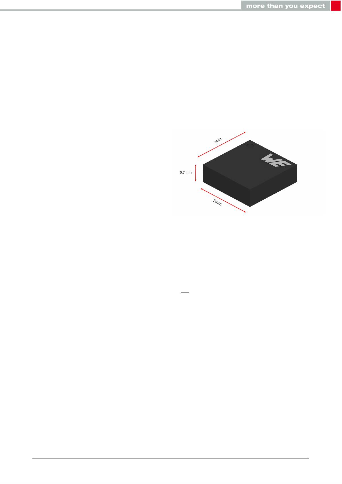
of the sensor is 2.0 mm×2.0 mm×0.7 mm. It is available in land grid array package (LGA).
1.2 Applications
• Industrial IoT and connected devices
• Industrial tools and factory equipment
• Vibration monitoring
• Tilt/inclination measurements
• Impact recognition and logging
1.3 Sensor features
• Selectable full scale:
• Output data rate:
• Bandwidth:
• Operating modes:
• Noise density:
• Current consumption:
• FIFO:
• Communication interface:
• Motion detection functionality:
• Embedded temperature sensor
±2g, ±4g, ±8g, ±16g
Up to 1600 Hz
400 Hz
High performance, normal, low power
90 µg /√Hz
High performance mode: 155µA
Normal mode: 58µA
Low power mode: 16µA
32-Level
I2C & SPI, two independent interrupt pins
Free-fall, wake-up, tap, activity, motion, orientation:
4D/6D/portrait/landscape
• Single data conversion on demand
• Self-test functionality
Acceleration sensor, Part Nr. 2533020201601
User manual version 2.0 © December 2020
www.we-online.com/sensors 7
Page 9
1.4 Block diagram
X-axis
Y-axis
Z-axis
Multiplexer
ADC
Embedded
Functions
Controller
Logic &
Interrupt
Amp
Temperature Sensor
Self testReference
Timming
Circuits
FIFO Buffer Free Fall
Tap
Detection
Orientation
Wake up
Stationary/
Motion
Activity/
Inactivity
Digital
Interface
SDA
SCL
Clock
Generator
CS
SAO
INT_0
INT_1
MEMS Element
The sensor is a MEMS based capacitive acceleration sensor with an integrated ASIC. The
MEMS element is capable of measuring both dynamic acceleration due to motion or vibration and also static acceleration due to gravity. The sensor measures the acceleration or
vibration through MEMS capacitive sensing principle. The MEMS element consists of a
fixed structure and movable structure. The movable structure is free to move in the direction
of acceleration applied i.e. X, Y and Z direction. The force induced on the MEMS element
produces change in the capacitance value that is proportional to the force exerted on it.
Without any force on the sensor the capacitors will have a nominal capacitance value in the
range of picofarad (pF). When an acceleration is applied, the change in the capacitance
value is induced in the range of femtofarad (fF). The induced analog signal is converted to
digital form using an analog to digital converter followed by filters and controller logic blocks.
The final acceleration data from the output register can be accessed through an I2C or SPI
digital communication interface using host processor.
1.5 Ordering information
Figure 1: Block diagram
WE order code Temperature Range Description
2533020201601 -40° C to +85° C Tape & reel packaging
Table 1: Ordering information
Acceleration sensor, Part Nr. 2533020201601
User manual version 2.0 © December 2020
www.we-online.com/sensors 8
Page 10

2 Sensor and electrical specifications
T=25°C, supply voltage VDD = 3.3V, unless otherwise stated.
2.1 Acceleration sensor specifications
Parameters Symbol
Axis 3
Measurement
range
a
RANGE
Output data rate ODR
Bandwidth f
BW
Resolution RES
RES
Sensitivity
accuracy
SEN
a_ACC
Sensitivity
change over
SEN
a_TC
temperature
performance /
a
normal mode
Low power
a
Test
conditions
User
selectable
User
selectable
User
selectable
High
mode
1
Min.
Typ. Max.
±2,±4,±8,±16
1,6 1600
0,08 400
14
12
-3 +3
0.01
1
Unit
g
Hz
Hz
bits
bits
%
%/°C
High
performance
Noise density
2
n
D
mode, ±2g,
ODR 200 Hz,
90 160
Low noise bit
enabled
0g Offset
accuracy
3
0g Offset change
over temperature
Resonant f
frequency f
a
OFF
a
TCO
res_X
res_Y
f
res_Z
-30 ±20 +30
-1 ±0.2 + 1
X 3.4
Y 3.4
Z 2.8
Table 2: Acceleration sensor specification
g: unit of acceleration, 1g = 9.81 m/s
1
Minimum and maximum values are based on characterization at 3σ.
2
Noise density is same for all ODRs. Low noise setting enabled.
2
µg /√Hz
mg
mg /°C
kHz
kHz
kHz
Acceleration sensor, Part Nr. 2533020201601
User manual version 2.0 © December 2020
www.we-online.com/sensors 9
Page 11
3
Values after calibration test and trimming.
2.1.1 Acceleration sensitivity parameter
Parameters
Sensitivity (±2g )
Sensitivity (±4g )
Sensitivity (±8g )
Sensitivity (±16g )
Sensitivity (±2g )
Sensitivity (±4g )
Sensitivity (±8g )
Sensitivity (±16g )
2
2
2
2
2
2
2
2
Symbol
SEN
a
SEN
a
SEN
a
SEN
a
SEN
a
SEN
a
SEN
a
SEN
a
Test conditions
High performance /
Normal mode
High performance /
Normal mode
High performance /
Normal mode
High performance /
Normal mode
Low power mode
Low power mode
Low power mode
Low power mode
Min.
1
Table 3: Acceleration sensitivity parameter
1
Minimum and maximum values are based on characterization at 3σ.
2
Sensitivity values after factory calibration test and trimming.
Typ. Max.
1
Unit
0.244 mg /digit
0.488 mg /digit
0.976 mg /digit
1.952 mg /digit
0.976 mg /digit
1.952 mg /digit
3.904 mg /digit
7.808 mg /digit
2.2 Temperature sensor specifications
Parameters
Measurement range
Sensitivity
Offset
Symbol
T
RANGE
SEN
SEN
T_12bit
T
OFF
T_8bit
Test conditions
8 bit resolution
12 bit resolution
Table 4: Temperature sensor specification
1
Minimum and maximum values are based on characterization at 3σ.
Min.
-40 +85 °C
-15 +15 °C
1
Typ. Max.
1
1 °C/LSB
0.0625 °C/LSB
Unit
Acceleration sensor, Part Nr. 2533020201601
User manual version 2.0 © December 2020
www.we-online.com/sensors 10
Page 12

2.3 Electrical specifications
Parameters
Operating supply
voltage
Operating supply
voltage for I/O pins
Current consumption in
high performance
mode
Current consumption in
normal mode
Current consumption in
low power mode
Current consumption in
power down mode
Digital input voltage -
high-level
Digital input voltage -
low-level
Symbol
V
DD
V
DD_IO
I
DD_HP
I
DD_NM
I
DD_LP
I
DD_PD
V
IH
V
IL
Test con-
ditions
ODR
200 Hz
ODR
200 Hz
ODR
200 Hz
1
Min.
1.7
Typ.
3.3
Max.
3.6 V
1.7 VDD+ 0.1 V
155
58
16
100 nA
0.8 * V
DD_IO
0.2 * V
DD_IO
1
Unit
µA
µA
µA
V
V
Digital output voltage -
high-level
Digital output voltage -
low-level
V
OH
V
OL
IOH= 4
2
mA
IOL= 4
2
mA
V
- 0.2 V
DD_IO
0.2 V
Table 5: Electrical specification
1
Minimum and maximum values are based on characterization at 3σ.
2
4 mA is the maximum driving capability i.e. the maximum DC current that can be sourced/-
sunk by digital pin in order to guarantee correct digital output voltage levels VOHandOL.
Acceleration sensor, Part Nr. 2533020201601
User manual version 2.0 © December 2020
www.we-online.com/sensors 11
Page 13
2.4 Absolute maximum rating
Parameter
Input voltage VDDpin
Input voltage V
DD_IO
pin
Input voltage SDA, SCL,
CS & SAO pins
Acceleration
Symbol
V
DD_Max
V
DD_IO_Max
V
IN_Max
a
MAX
Test conditions
for 0.5 ms
Min.
-0.3 4.8 V
-0.3 4.8 V
-0.3 V
Table 6: Absolute maximum rating
1
Minimum and maximum values are based on characterization at 3σ.
Supply voltage on any pin should never exceed 4.8 V
2.5 General information
1
Max.
DD_IO
1
Unit
+ 0.3 V
3000 g
Parameters Values
Operating temperature -40°C to +85°C
Storage temperature -40°C to +125°C
Communication interface I2C & SPI
Moisture sensitivity level (MSL) 3
Electrostatic discharge protection(HBM) 2 kV
Table 7: General information
The device is susceptible to damage by electrostatic discharge (ESD). Always
use proper ESD precautions when handling. Improper handling of the device
can cause performance degradation or permanent damage to the part
Acceleration sensor, Part Nr. 2533020201601
User manual version 2.0 © December 2020
www.we-online.com/sensors 12
Page 14
3 Pinning description
1
4
2
3
5 6
7
8
9
10
1112
SCL
CS
SAO
SDA
NC
GND INT_1
INT_0
RSVD
GND
VDD
VDD_IO
Figure 2: Pinout (top view)
No Function Description Input/Output
1 SCL I2C /SPI serial clock Input
2 CS I2C enable/disable, SPI chip select Input
3 SAO
I2C device address selection, SPI
serial data output
Input/Output
4 SDA I2C serial data, SPI serial data input Input/Output
5 NC No connection 6 GND Negative supply voltage Supply
7 RSVD Reserved, connect to GND Input
8 GND Negative supply voltage Supply
9 VDD Positive supply voltage Supply
10 VDD_IO Positive supply voltage for I/O pins Supply
11 INT_1 Interrupt pin 1 Input/Output
12 INT_0 Interrupt pin 0 Output
Table 8: Pin description
Acceleration sensor, Part Nr. 2533020201601
User manual version 2.0 © December 2020
www.we-online.com/sensors 13
Page 15

4 Application circuit
12 11 10
2
3
4 5 6 7
8
9
SCL
1
CS
SAO
SDA
VDD_IO
VDD
10 µF 100 nF
GND
RSVD
GNDNC
100 nF
VDD_IO
INT_0 INT_1
VDD
SDA
SCL
Rp Rp
I²C Bus configuration
4 Wire SPI configuration
SAO
MOSI
MISO
SDA
Rp – Pull up resistor
CS
SS
SCL
CLK
Figure 3: Electrical connection (top view)
A positive supply voltage is applied to the sensor through VDD pin and I/O supply voltage for
digital interface through VDD_IO. The decoupling capacitor of 100 nF and 10µF in parallel
is highly recommended and should be placed as close as possible to the VDD pin. Communication is still possible, even if the supply voltage to theVDD pin is removed but maintaining
the VDD_IO. In this case, measurement chain of the sensor is not active.
The CS pin shall be connected to SS (slave select) pin on the controller side to enable SPI
communication interface. The CS pin shall be connected to VDD_IO in order to enable the
I2C communication interface. It is possible to have two I2C slave addresses by connecting
SAO pin either to VDD_IO or GND. In the above connection the SAO pin is connected to
VDD_IO. Rpare the recommended pull up resistors for I2C communication interface which
should be connected parallel between I/O supply voltage VDD_IO and SCL and SDA pins.
The SAO and CS pins are internally pulled up. The internal pull up resistor values of SAO
and CS pins for different supply voltage of the I/O pins are given below in table 9.
VDD_IO Resistor value of SAO and CS (Typ.)
1.7V 54.4 KΩ
1.8V 49.2 KΩ
2.5V 30.4 KΩ
3.6V 20.4 KΩ
Table 9: Internal pull up values (typ) for SAO and CS pins
Acceleration sensor, Part Nr. 2533020201601
User manual version 2.0 © December 2020
www.we-online.com/sensors 14
Page 16
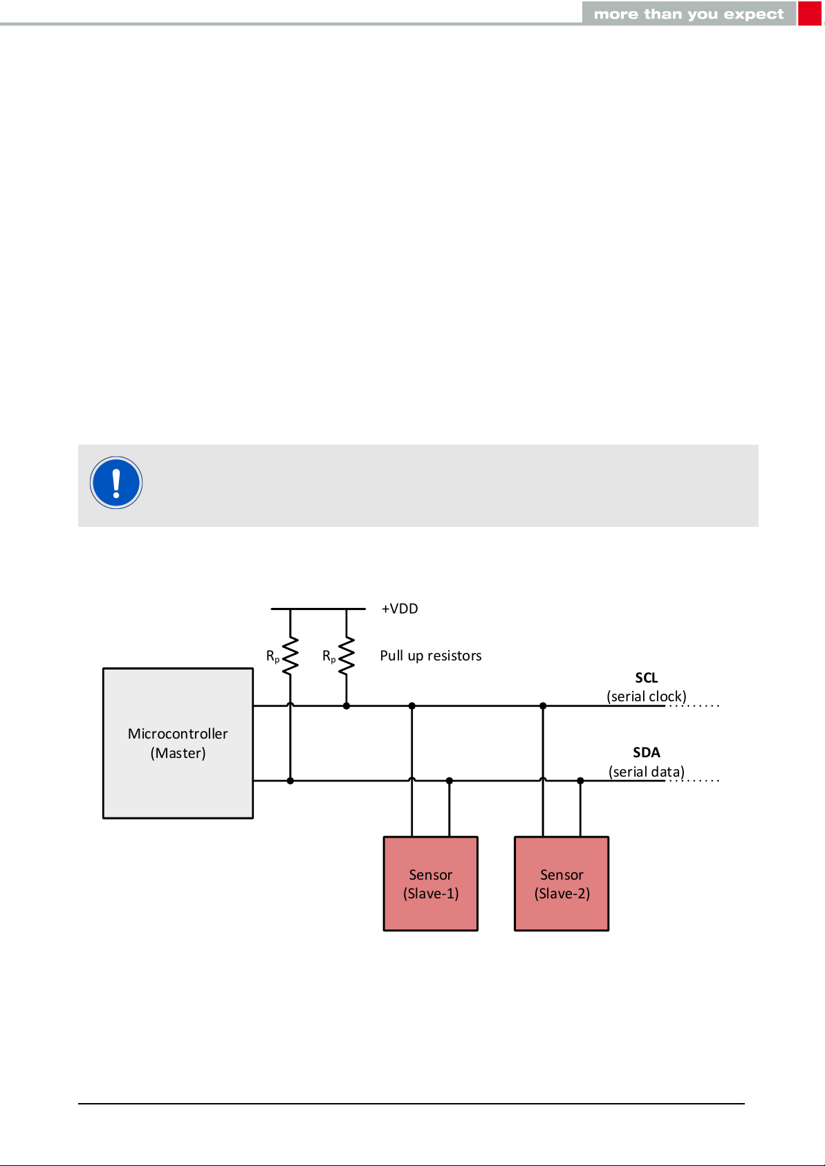
5 Inter-Integrated Circuit (I2C)
Microcontroller
(Master)
R
p
R
p
Sensor
(Slave-1)
Sensor
(Slave-2)
+VDD
SCL
(serial clock)
SDA
(serial data)
Pull up resistors
The acceleration sensor supports standard I2C (Inter-IC) bus protocol. Further information
of the I2C interface can be found at https://www.nxp.com/docs/en/user-guide/UM10204.pdf.
I2C is a serial 8-bit protocol with two-wire interface which supports communication between
different ICs. For example, between the microcontroller and other peripheral devices.
5.1 General characteristics
A serial data line (SDA) and a serial clock line (SCL) are required for the communication
between the devices connected via I2C bus. Both SDA and SCL lines are bidirectional. The
output stages of devices connected to the bus must have an open-drain or open-collector.
Hence, the SDA and SCL lines are connected to a positive supply voltage via pull-up resistors. In I2C protocol, the communication is realized through master-slave principle. The
master device generates the clock pulse, a start command and a stop command for the data
transfer. Each connected device on the bus is addressable via a unique address. Master
and slave can act as a transmitter or a receiver depending upon whether the data needs to
be transmitted or received.
The sensor behaves like a slave device on the I2C bus
Figure 4: Master-slave concept
Acceleration sensor, Part Nr. 2533020201601
User manual version 2.0 © December 2020
www.we-online.com/sensors 15
Page 17
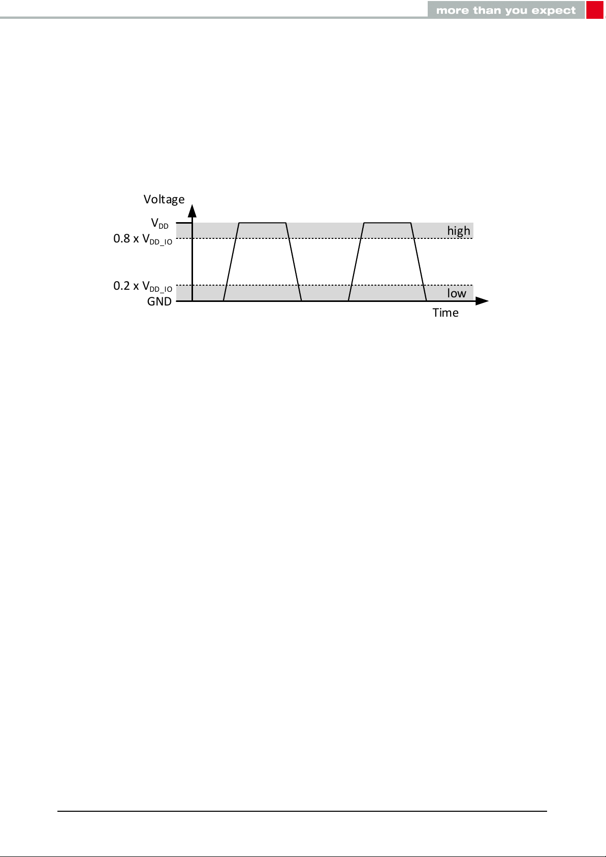
5.2 SDA and SCL logic levels
Voltage
low
high
Time
V
DD
GND
0.2 x V
DD_IO
0.8 x V
DD_IO
The positive supply voltage to which SDA and SCL lines are pulled up (through pull-up
resistors), in turn determines the high level input for the slave devices. The sensor has
separate supply voltage VDD_IO for the SDA and SCL lines. The logic high ’1’ and logic low
’0’ levels for the SDA and SCL lines then depend on the VDD_IO. Input reference levels for
the acceleration sensor are set as 0.8 * VDD_IO (for logic high) and 0.2 * VDD_IO (for logic
low). See in figure 5.
Figure 5: SDA and SCL logic levels
5.3 Communication phase
5.3.1 Idle state
During the idle state, the bus is free and both SDA and SCL lines are in logic high ’1’ state.
5.3.2 START(S) and STOP(P) condition
Data transfer on the bus starts with a START command, which is generated by the master.
A start condition is defined as a high-to-low transition on the SDA line while the SCL line is
held high. The bus is considered busy after the start condition.
Data transfer on the bus is terminated with a STOP command, which is also generated by
the master. A low-to-high transition on the SDA line, while the SCL line being high is defined
as a STOP condition. After the stop condition, the bus is again considered free and is in idle
state. Figure 6 shows the I2C bus START and STOP conditions.
Master can also send a REPEATED START (SR) command instead of STOP command.
REPEATED START condition is same as the START condition.
Acceleration sensor, Part Nr. 2533020201601
User manual version 2.0 © December 2020
www.we-online.com/sensors 16
Page 18
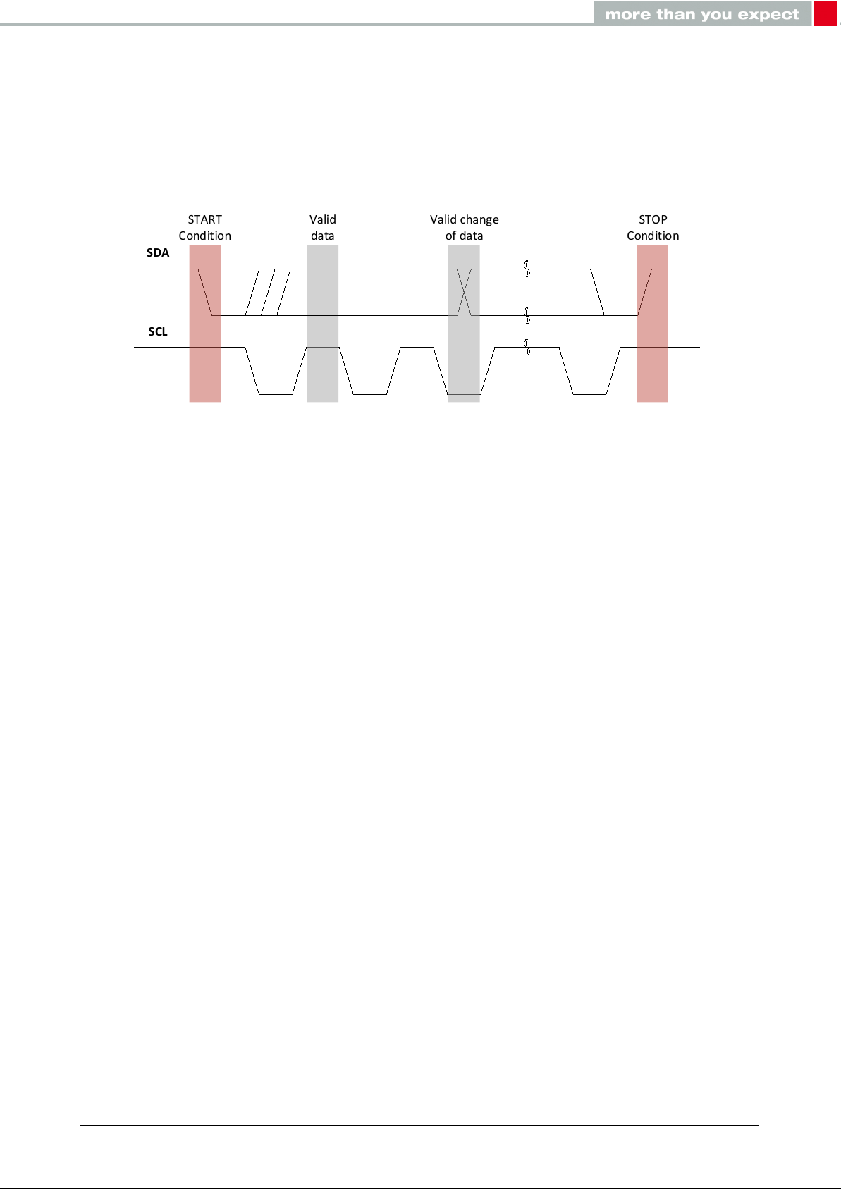
5.3.3 Data validity
SDA
SCL
START
Condition
STOP
Condition
Valid
data
Valid change
of data
After the start condition, one data bit is transmitted with each clock pulse. The transmitted
data is only valid when the SDA line data is stable (high or low) during the high period of the
clock pulse. High or low state of the data line can only change when the clock pulse is in low
state.
Figure 6: Data validity, START and STOP condition
5.3.4 Byte format
Data transmission on the SDA line is always done in bytes, with each byte being 8-bits long.
Data is transmitted with the most significant bit (MSB) followed by other bits.
If the slave cannot receive or transmit another complete byte of data, it can force the master
into a wait state by holding SCL LOW. Data transfer continues when the slave is ready which
is indicated by releasing the SCL pin.
5.3.5 Acknowledge(ACK) and No-Acknowledge(NAACK)
Each byte transmitted on the data line must follow an Acknowledge bit. The receiver (master or slave) generates an Acknowledge signal to indicate that the data byte was received
successfully and ready to receive next data byte.
After one byte is transmitted, the master generates an additional Acknowledge clock pulse
to continue the data transfer. The transmitter releases the SDA line during this clock pulse
so that the receiver can pull the SDA line to low state in such a way that the SDA line
remains stable low during the entire high period of the clock pulse. It is considered as an
Acknowledge signal.
If the receiver does not want to receive any further byte, it will not pull down the SDA line
and it remains in stable high state during the entire clock pulse. It is considered as a NoAcknowledge signal and the master can generate either a stop condition to terminate the
data transfer or a repeated start condition to initiate a new data transfer.
Acceleration sensor, Part Nr. 2533020201601
User manual version 2.0 © December 2020
www.we-online.com/sensors 17
Page 19
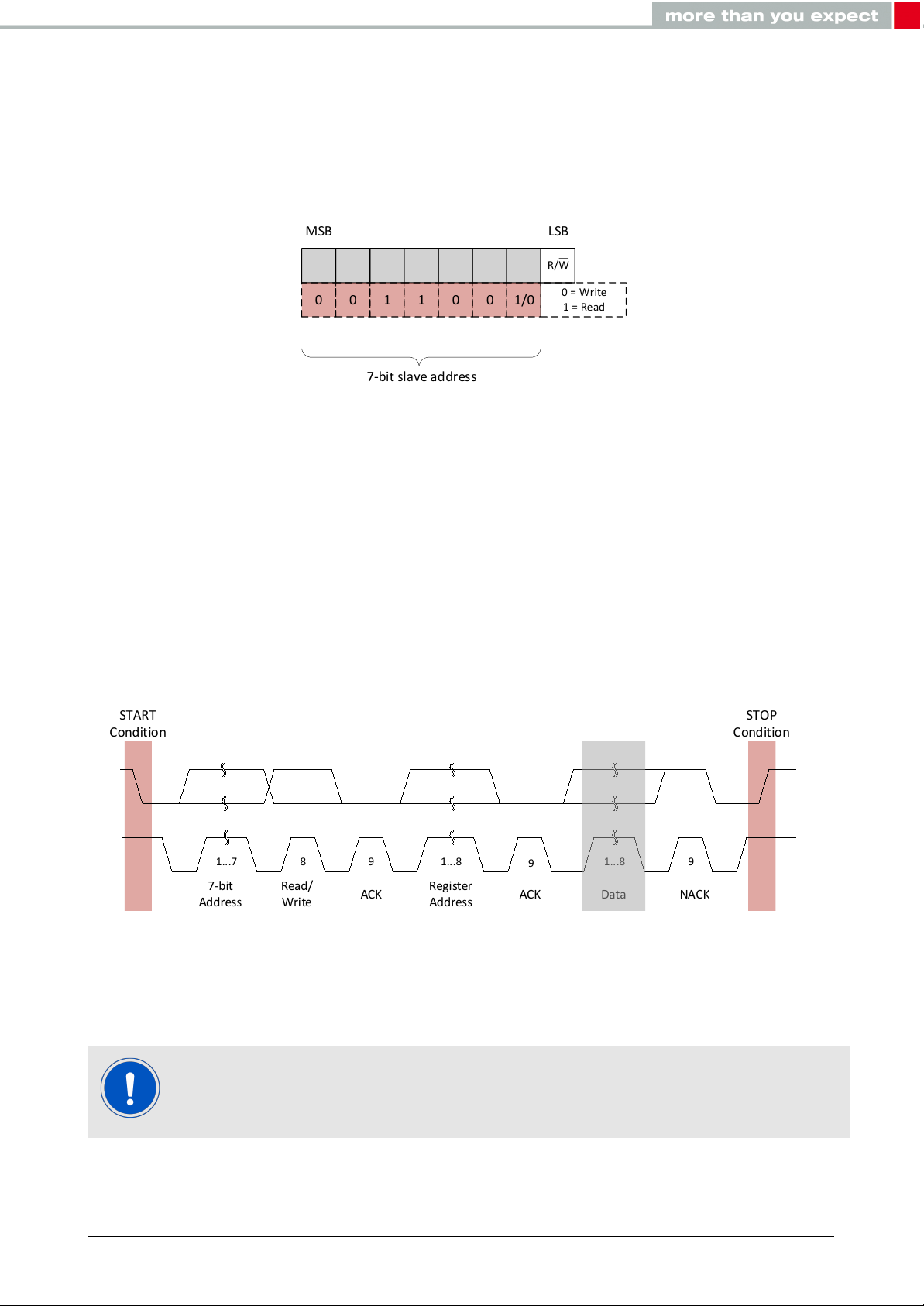
5.3.6 Slave address for the sensor
R/W
7-bit slave address
LSBMSB
0 0 1 1 0 0 1/0
0 = Write
1 = Read
START
Condition
STOP
Condition
1...7 8 9 1...8
9
1...8 9
7-bit
Address
Read/
Write
ACK
Register
Address
ACK NACKData
The slave address is transmitted after sending the start condition. Each device on the I2C
bus has a unique address. Master selects the slave by sending corresponding slave address
after the start condition. A slave address is a 7 bits long followed by a Read/Write bit.
Figure 7: Slave address format
The 7-bit slave address of the acceleration sensor is 001100xb. LSB of the 7-bit slave
address can be modified with the SAO pin. If SAO is connected to positive supply voltage
i.e. LSB is ’1’, making 7-bit slave address 0011001b (0x19). If SAO is connected to ground
i.e. LSB is ’0’, making 7-bit address 0011000b (0x18).
The R/W bit determines the data direction. A ’0’ indicates a write operation (transmission
from master to slave) and a ’1’ indicates a read operation (data request from slave).
Figure 8: Complete data transfer
Acceleration sensor, Part Nr. 2533020201601
User manual version 2.0 © December 2020
7-bit slave address of the acceleration sensor is 001100xb. LSB of the 7-bit
slave address depends on the SAO pin connection
www.we-online.com/sensors 18
Page 20
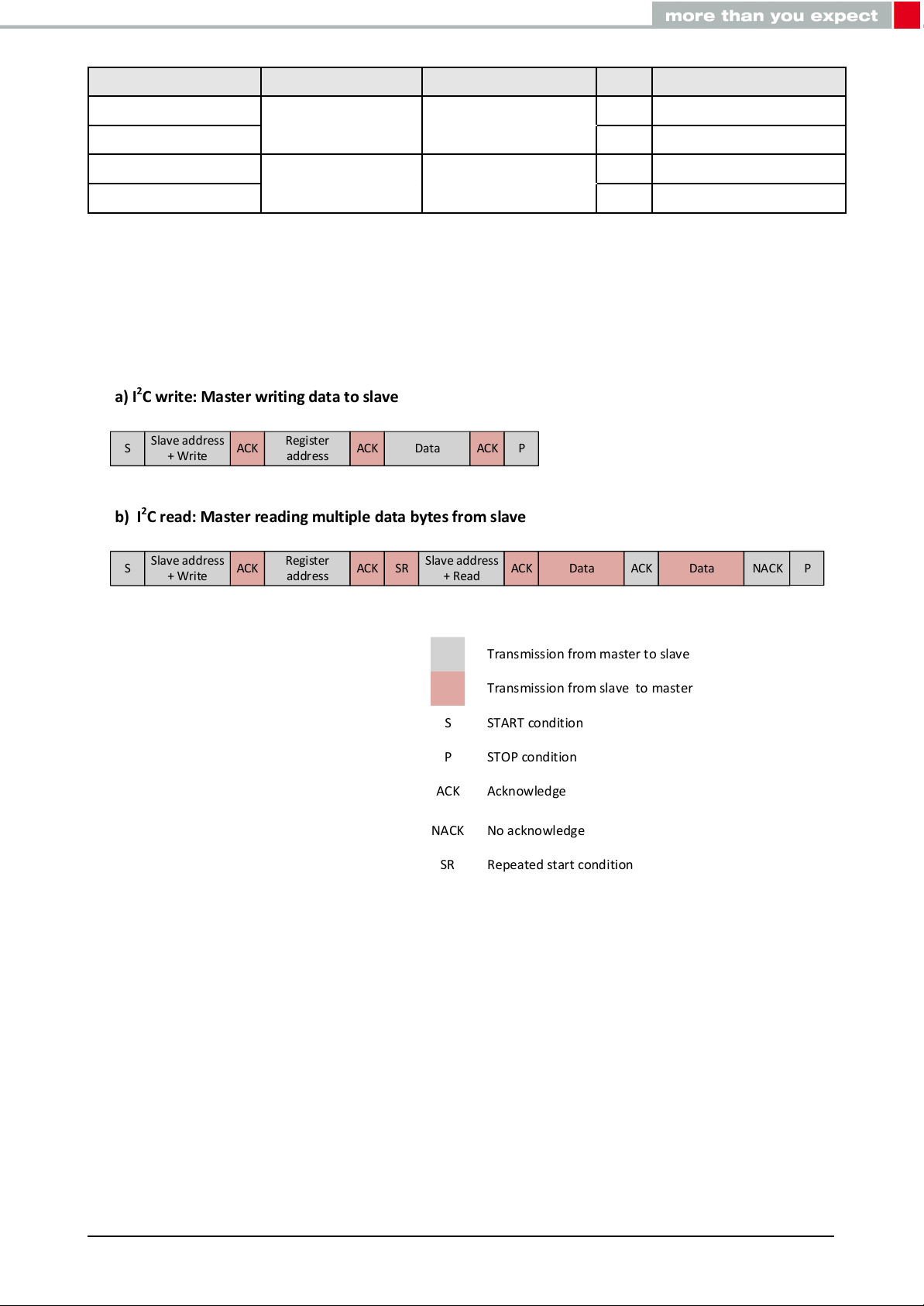
Slave address[6:1]
S
Slave address
+ Write
ACK
Register
address
DataACK ACK P
S
Slave address
+ Write
ACK
Register
address
Slave address
+ Read
ACK ACK
P
SR Data Data NACKACK
Transmission from master to slave
Transmission from slave to master
S
P
ACK
NACK
SR
START condition
STOP condition
Acknowledge
No acknowledge
Repeated start condition
a) I2C write: Master writing data to slave
b) I2C read: Master reading multiple data bytes from slave
Slave address[0]
7-bit slave address R/W Slave address + R/W
001100 0 00110000 (0x30)
SAO = 0
001100
001100 0 00110010 (0x32)
SAO = 1
001100
Table 10: Slave address and Read/Write commands
5.3.7 Read/Write operation
0011000 (0x18)
1 00110001 (0x31)
0011001 (0x19)
1 00110011 (0x33)
Figure 9: Write and read operations of the sensor
Once the slave-address and data direction bit is transmitted, the slave acknowledges the
master. The next byte is transmitted by the master, which must be a register-address of the
sensor. It indicates the address of the register where data needs to be written to or read
from.
After receiving the register address, the slave sends an Acknowledgement (ACK). If the
master is still writing to the slave (R/W bit = 0), it will transmit the data to slave in the same
direction. If the master wants to read from the addressed register (R/W bit =1), a repeated
start (SR) condition must be transmitted to the slave. Master acknowledges the slave after
Acceleration sensor, Part Nr. 2533020201601
User manual version 2.0 © December 2020
www.we-online.com/sensors 19
Page 21
receiving each data byte. If the master no longer wants to receive further data from the slave,
it would send No-Acknowledge (NACK). Afterwards, master can send a STOP condition to
terminate the data transfer. Figure 9 shows the writing and reading procedures between the
master and the slave device (sensor).
5.4 I2C timing parameters
Standard mode Fast mode
Parameter Symbol
Min Max Min Max
Unit
SCL clock frequency f
LOW period for SCL clock t
HIGH period for SCL clock t
LOW_SCL
HIGH_SCL
Hold time for START
condition
Setup time for (repeated)
START condition
SDA setup time t
SDA data hold time t
Setup time for STOP
condition
Bus free time between
STOP and START condition
Table 11: I2C timing parameters
SCL
t
HD_S
f
SCL
SU_SDA
HD_SDA
t
SU_P
t
BUF
0 100 0 400 kHz
4.7 1.3 µs
4.0 0.6 µs
4 0.6 µs
4.7 0.6 400 µs
250 100 ns
0 3.45 0 0.9 µs
4 0.6 µs
4.7 1.3 µs
Acceleration sensor, Part Nr. 2533020201601
User manual version 2.0 © December 2020
www.we-online.com/sensors 20
Page 22
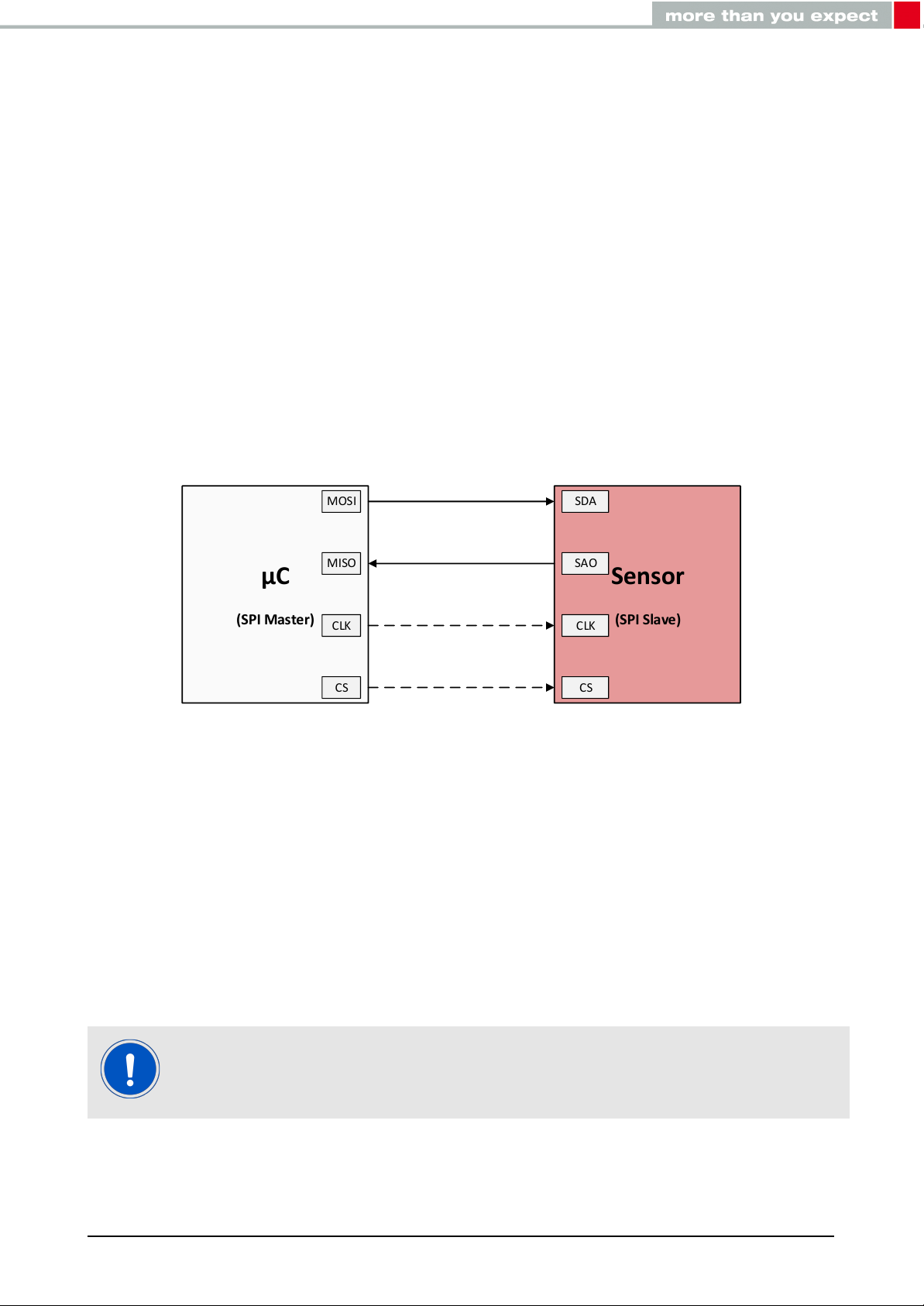
6 Serial Peripheral Interface (SPI)
µC
(SPI Master)
Sensor
(SPI Slave)
MOSI
MISO
CLK
CS
SDA
SAO
CLK
CS
Serial Peripheral Interface (SPI) is a synchronous serial communication bus system for the
communication between host microcontroller and other peripheral ICs such as ADCs, EEPROMs, sensors, etc. SPI is a full-duplex master-slave based interface allowing the communication to happen in both directions simultaneously. The data from the master or the slave
is synchronized either on the rising or falling edge of clock pulse. SPI can be either 4-wire or
3-wire interface. 4-wire interface consists of two signal lines and two data lines. All of these
bus lines are unidirectional.
1. Clock (SCL)
2. Chip select (CS)
3. Master out, slave in (MOSI)
4. Master in, slave out (MISO)
Figure 10: SPI Interface
Master generates the clock signal and is connected to all slave devices. Data transmission
between the master and salves is synchronized to the clock signal generated by the master.
One master can be connected to one or more slave devices. Each slave device is addressed
and controlled by the master via individual chip select (CS) signals. CS is controlled by the
master and is normally an active low signal.
MOSI and MISO are data lines. MOSI transmits data from the master to the slave. MISO
transmits data from the slave to the master.
The acceleration sensor supports 4-wire SPI communication protocol
Acceleration sensor, Part Nr. 2533020201601
User manual version 2.0 © December 2020
www.we-online.com/sensors 21
Page 23
6.1 Data transfer
Communication begins when the master selects a slave device by pulling the CS line to
LOW. The clock and data lines (MOSI/MISO) are available for the selected slave device.
Data stored in the specific shift registers are exchanged synchronously between master and
the slave through MISO and MOSI lines. The data transmission is over when the chip select
line is pulled up to the HIGH state. 4-wire SPI uses both data lines for the synchronous data
exchange in both the direction. 3-wire SPI shares a single data line for the data transfer,
where the master and slave alternate their transmitter and receiver roles synchronously.
6.2 Communication modes
In SPI, the master can select the clock polarity (CPOL) and clock phase (CPHA). The CPOL
bit sets the polarity of the clock signal during the idle state. The CPHA bit selects the clock
phase. Depending on the CPHA bit, the rising or falling clock edge is used to sample and
shift the data. Depending on the CPOL and CPHA bit selection in the SPI control registers,
four SPI modes are available as per table12. In order to ensure proper communication,
master and the slave must be set to same communication modes.
CPOL CPHA Description
0 0 Clock polarity LOW in idle state; Data sampled on the rising clock edge
0 1 Clock polarity LOW in idle state; Data sampled on the falling clock edge
1 1 Clock polarity HIGH in idle state; Data sampled on the falling clock edge
1 0 Clock polarity HIGH in idle state; Data sampled on the rising clock edge
Table 12: SPI communication modes
Acceleration sensor, Part Nr. 2533020201601
User manual version 2.0 © December 2020
www.we-online.com/sensors 22
Page 24
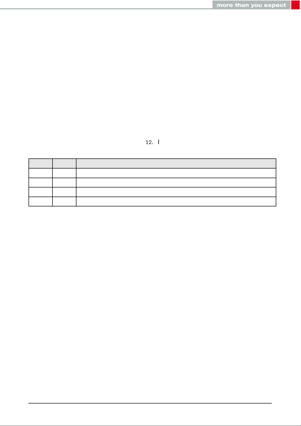
6.3 Sensor SPI Communication
7- bit register address
R/W
LSBMSB
A[6]
A[5] A[4] A[3] A[2] A[1] A[0]
0 = Write
1=Read
R/W A[6] A[5] A[4] A[3] A[2] A[1] A[0] DI[7] DI[6] DI[5] DI[4] DI[3] DI[2] DI[1] DI[0]
DO[7] DO[6] DO[5] DO[4] DO[3] DO[2] DO[1] DO[0]
CS
SCK
SDA
SAO
4-Wire SPI of this sensor uses following lines: SDA (data input, MOSI), SAO (data output,
MISO), SCL (serial clock) and CS (chip select). For more information, please refer to pin
description in the section 3.
CS is pulled LOW by the master at the start of communication. The SCL polarity is HIGH in
the idle state (CPOL = 1). The data lines (SDA & SAO) are sampled at the falling clock edge
and latched at the rising clock edge (CPHA = 1). Data is transmitted with MSB first and the
LSB last.
SPI read and write operations are completed in 2 or more bytes (multiple of 16 or more clock
pulses). Each block consists of a register address byte and a data byte. The first byte is the
register address. In the SPI communication, the register address is specified in the 7-bits
and the MSB of the register address is used as an SPI read/write bit (Figure11). When R/W
is ’0’, the data is written on to the sensor. When ’1’, the data is read from the sensor.
Figure 11: SPI register address
The next bytes of data, depending on the R/W bit, is either written to or read from the indexed
register. Figure12shows the complete SPI data transfer protocol.
Figure 12: 4-wire SPI data transfer (CPOL = 1, CPHA = 1)
Acceleration sensor, Part Nr. 2533020201601
User manual version 2.0 © December 2020
www.we-online.com/sensors 23
Page 25
6.3.1 SPI write operation
Register address
A[6]
A[5] A[4] A[3] A[2] A[1] A[0]
R/WStart
CS =
LOW
0
DI
[6]
DI
[5]
DI
[4]
DI
[3]
DI
[2]
DI
[1]
DI
[0]
DI
[7]
Data to be written
Stop
CS =
HIGH
Register address
A[6] A[5] A[4] A[3] A[2] A[1] A[0]
R/WStart
CS =
LOW
1
DO
[6]
DO
[5]
DO
[4]
DO
[3]
DO
[2]
DO
[1]
DO
[0]
DO
[7]
Data from indexed register
Stop
CS =
HIGH
The write operation starts with the CS = LOW and sending the 7-bit register address with
R/W bit = ’0’ (write command). Next byte is the data byte that is the data to be written to the
indexed register. Several write command pairs can be sent without raising the CS back to
HIGH. The operation is ended with CS = HIGH. The SPI write protocol is shown in the figure
13
.
Figure 13: SPI write protocol
6.3.2 SPI read operation
The read operation starts with the CS = LOW and sending the 7-bit register address with
R/W bit = ’1’ (read command). Data is sent out from the sensor through the SAO line. The
SPI read protocol is shown in the figure14.
Figure 14: SPI read protocol
During multiple read/write operation, the register address is automatically incremented after each block. This feature is enabled by default with the bit
IF_ADD_INC set to ’1’ in the CTRL_2 register.
Acceleration sensor, Part Nr. 2533020201601
User manual version 2.0 © December 2020
www.we-online.com/sensors 24
Page 26
6.3.3 SPI timing parameters
Table13shows general SPI timing parameters. They are subject to VDD and the operating
temperature.
Parameter Symbol Min Max Unit
SCL clock frequency f
SCL
10
(1)
MHz
SPI clock cycle t
CS setup time t
CS hold time t
SDA input setup time t
SDA input hold time t
SAO valid output time t
SAO output hold time t
SAO output disable time t
SCL
SU_CS
h_CS
SU_SDA
h_SDA
v_SAO
h_SAO
dis_SAO
Table 13: SPI timing parameters
1. Recommended maximum SPI clock frequency for ODR ≤ 50 Hz is 8 MHz
100 ns
6 ns
6 ns
5 ns
15 ns
50 ns
9 ns
50 ns
Acceleration sensor, Part Nr. 2533020201601
User manual version 2.0 © December 2020
www.we-online.com/sensors 25
Page 27

7 Sensor specific parameters
7.1 Sensitivity
Sensitivity is defined as the ratio of change in input acceleration to the change in the output signal. The unit of sensitivity is typically expressed in mg/digit. It can be measured
by pointing the sensor horizontally downwards, an acceleration of 1g is measured due to
earth’s gravity (9.807 m/s2). Similarly by pointing sensor horizontally upwards (rotation of
180 degree), again an acceleration of 1g is measured due to earth’s gravity (9.807 m/s2). By
subtracting the larger measured output value from the smaller measured output value and
dividing by two gives the actual sensitivity of the acceleration sensor.
The sensitivity value will drift over time and temperature.
Sensitivity =
larger value - smaller value
(1)
2
7.2 0 g Level offset
0 g level is the output level when there is no acceleration or motion acting on the sensor i.e.
zero input. A sensor placed on a perfect horizontal plane will give 0 g output on X-axis and
Y-axis but 1 g on Z-axis. The deviation of an actual output value from the ideal value gives
the 0 g level offset. 0 g offset value is influenced by external parameters like temperature
and stress. External stress on the sensor will affect the sensor performance significantly.
The 0 g level offset will also drift over temperature.
External stress: Vias under the sensor on a PCB, PCB warpage, external
mechanical stress to the sensor.
7.3 Noise density
Noise density of the sensor is expressed as µg /√Hz. Noise density of the acceleration
sensor is dependent on the output data rate. The values are expressed in the chapter9.
The noise of the acceleration sensor is determined by the equivalent noise bandwidth of the
output filter and coefficient of the filter order. In general, the noise density is determined by
the equation:
Noise density =
Acceleration sensor, Part Nr. 2533020201601
User manual version 2.0 © December 2020
www.we-online.com/sensors 26
√
Bandwidth * filter coefficent
rms noise
[µg/√Hz] (2)
Page 28

8 Quick start guide
This chapter describes the start up sequence of the acceleration sensor.
8.1 Power supply
The sensor has two individual supply voltage pins.
• VDD is main supply voltage
• VDD_IO is the I/O pin supply voltage for the digital I2C or SPI communication interface
It should be noted that VDD level should never be lower than VDD_IO i.e. proper power up
should be VDD > VDD_IO. It is possible to remove VDD by keeping VDD_IO pin without
communication interruption but the measurement chain of the sensor is turned off i.e. VDD
= 0 with VDD_IO "high" is allowed. In this case, the measurement chain is turned off but the
communication to the sensor is possible without interruption.
Power up sequence should be VDD > VDD_IO .
8.2 Boot status
By proper powering up of the sensor with correct voltage level to the respective pins, the
sensor enters into a 20 ms boot sequence to load the trimming parameters. After completion of the boot up sequence the sensor automatically enters to power down mode.
It is also possible to initiate the boot sequence manually by the user. It is performed by
setting the BOOT bit of the CTRL_2 register to ’1’, then the boot sequence is initiated and
trimming parameters are reloaded. In this case, the device operation mode does not change
after boot procedure. No toggle of the power is required and the content of the device control
registers is not modified.
During the 20ms boot sequence the registers are not accessible.
The boot status signal is identified by setting the INT1_BOOT bit of the CTRL_5 register
to ’1’. When the sensor is in boot sequence, INT_1 interrupt pin is driven high. Similarly
when the boot sequence is completed, INT_0 interrupt pin is driven low.
Acceleration sensor, Part Nr. 2533020201601
User manual version 2.0 © December 2020
www.we-online.com/sensors 27
Page 29
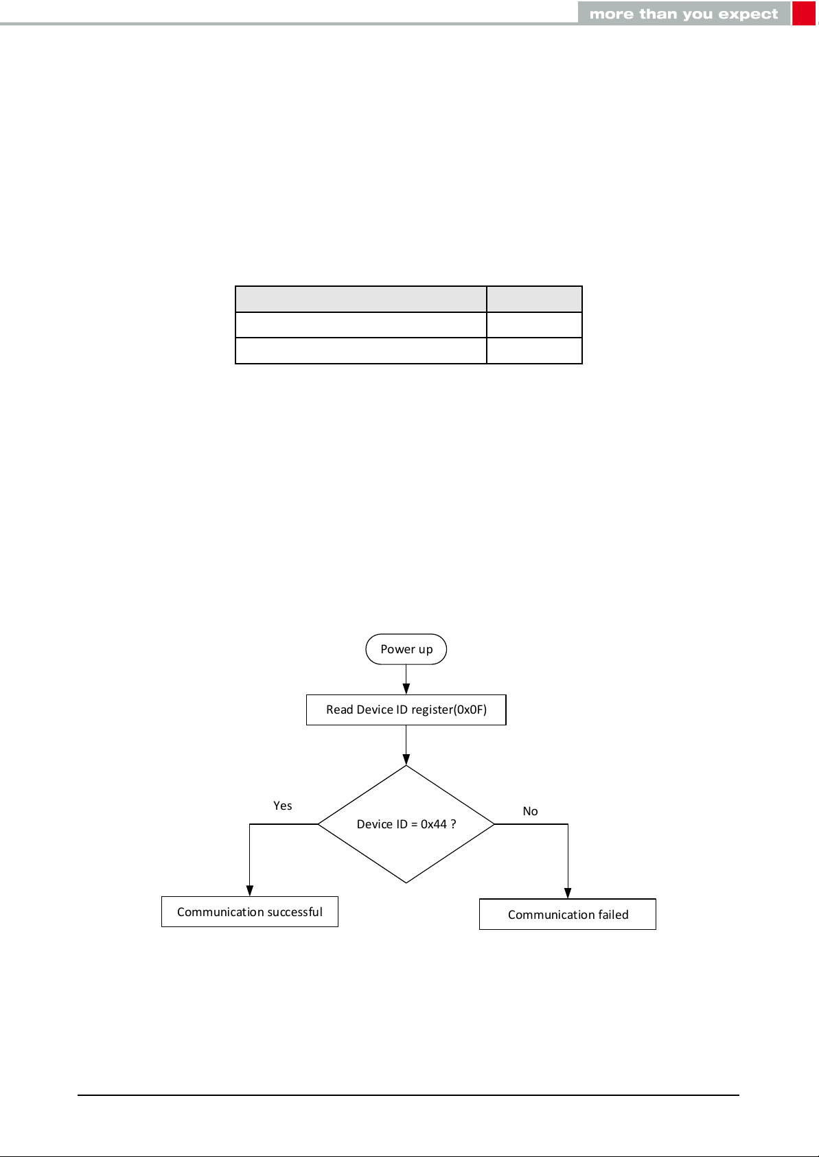
8.2.1 Soft reset
Power up
Read Device ID register(0x0F)
Device ID = 0x44 ?
Communication successful
Communication failed
Yes
No
If required, the soft reset of the sensor is possible. It resets the default value of the control
registers. The soft reset procedure will take 5 µs.
The below steps should be considered for setting the BOOT bit manually:
1. Write SOFT_RESET bit to ’1’
2. Wait for 5 µs
3. Write BOOT bit to ’1’
4. Wait for 20 ms
Parameter Time
Boot sequence 20 ms
Soft reset duration 5 µs
Table 14: Time consumption
8.3 Flow chart
8.3.1 Communication check
After proper powering of the sensor, the first step is to check the communication of the
sensor with an I2C or SPI communication interface. It can be verified by reading the value
of DEVICE_ID register(0x0F). If the value from the DEVICE_ID register(0x0F) is 0x44, then
the communication to the sensor is successful.
Acceleration sensor, Part Nr. 2533020201601
User manual version 2.0 © December 2020
www.we-online.com/sensors 28
Figure 15: Communication check
Page 30
8.3.2 Sensor in operation with high performance mode
Sensor in power down
mode
Enable high performance mode
Select output data rate: 200 Hz
Select bandwidth: ODR/2 Hz
Select full scale: ± 16g
Enable block data update
Enable automatic address increment
CTRL_2(0x21)
CTRL_1(0x20)
Enable low power mode for
lowest power consumption
If
DRDY bit =1?
Read DRDY bit in status
register
Request data from output register
XL (0x28)
Read XL, XH, YL, YH, ZL, ZH
X_16 = XH & XL
Y_16 = YH & YL
Z_16 = ZH & ZL
Request data from output register
0x28 and receive data from 0x28,
0x29, 0x2A, 0x2B, 0x2C and 0x2D
Save data from output register
0x28, 0x29, 0x2A, 0x2B, 0x2C and
0x2D
Concatenation of 8 bit ouput values
to get 16 bit output values
Yes
No
No data in output register
CTRL_6(0x25)
Status register(0x27)
Acceleration value in mg
X_shift = X_16 >>2
Y_shift = Y_16 >>2
Z_shift = Z_16 >>2
X axis = X_Shift * 1.952
Y axis = Y_Shift * 1.952
Z axis = Z_Shift * 1.952
Multiplying the sensitivity value for
the selected full scale range ±16 g
Steps can
be
performed
once
Steps can
be
performed
in loops
Normal/high performance mode:
14-bit resolution output data
Right shift the data by 2 bits
In case of low power mode enabled:
12 bit resolution output data
Right shift the data by 4 bits
The following flow chart is an initialization example to operate the sensor in high performance
mode with output data rate of 200 Hz.
Figure 16: Sensor in operation with high performance mode
Acceleration sensor, Part Nr. 2533020201601
User manual version 2.0 © December 2020
www.we-online.com/sensors 29
Page 31

In order to set the sensor in one of the operation modes, the sensor needs to be initialized.
The initialization of the sensor can be performed by defining output data rate, full scale
setting and filtering path. After initializing the sensor, it is recommended to check if the
data samples are available in the output registers. It can be verified by reading DRDY bit in
STATUS register(0x27). If the DRDY bit is enabled, the output data of three axes from the
registers 0x28, 0x29, 0x2A, 0x2B, 0x2C and 0x2D are available. The acceleration value of
the sensor is obtained by multiplying output data with respective sensitivity parameter value
based on the selected full scale range. Sensitivity parameter values for different full scale
ranges are mentioned in the table 3.
8.3.3 Sensor in operation with single data conversion mode
The following flow chart is an initialization example to operate the sensor in single data
conversion mode with output data rate of 200 Hz. In this example, single data conversion is
triggered by writing SLP_MODE_1 bit to ’1’. To set the sensor in to operation, normal and
low power mode can be selected. High performance mode cannot be selected in single data
conversion mode.
In single data conversion mode either normal mode or low power mode can be
selected.
High performance mode cannot be selected with single data conversion mode
Acceleration sensor, Part Nr. 2533020201601
User manual version 2.0 © December 2020
www.we-online.com/sensors 30
Page 32
Sensor in power down
mode
Enable normal mode
Select output data rate: 200 Hz
Select bandwidth: ODR/2 Hz
Select full scale: ± 16g
Enable block data update
Enable automatic address increment
CTRL_2(0x21)
CTRL_1(0x20)
Enable low power mode for
lowest power consumption
If
DRDY bit =1?
Set SLP_MODE_SEL bit = 1
Request data from output register
XL (0x28)
Read XL, XH, YL, YH, ZL, ZH
X_16 = XH & XL
Y_16 = YH & YL
Z_16 = ZH & ZL
Request data from output register
0x28 and receive data from 0x28,
0x29, 0x2A, 0x2B, 0x2C and 0x2D
Save data from output register
0x28, 0x29, 0x2A, 0x2B, 0x2C and
0x2D
Concatenation of 8 bit ouput values
to get 16 bit output values
Yes
No
No data in the output register
CTRL_6(0x25)
CTRL_3(0x22)
Start of single data conversion.
After conversion, the SLP_MODE_1
bit automatically set to 0
Acceleration value in mg
X_shift = X_16 >>2
Y_shift = Y_16 >>2
Z_shift = Z_16 >>2
X axis = X_Shift * 1.952
Y axis = Y_Shift * 1.952
Z axis = Z_Shift * 1.952
Normal mode enabled:
14-bit resolution output data
Right shift the data by 2 bits
In case of low power mode enabled:
12 bit resolution output data
Right shift the data by 4 bits
Multiplying the sensitivity value for
the selected full scale range ±16 g
Set SLP_MODE_1 = 1
CTRL_3(0x22)
Trigger single data conversion when
SLP_MODE_1 = 1
5 ms delay
New data needed?
Yes
No new data available in the
output registers
No
Steps can
be
performed
once
Steps can
be
performed
in loops
Figure 17: Sensor in operation with single data conversion mode
Acceleration sensor, Part Nr. 2533020201601
User manual version 2.0 © December 2020
www.we-online.com/sensors 31
Page 33
9 Operating modes
The acceleration sensor can be operated in three different operation modes which provides
different combination of noise and current consumption values. These operating modes are
selected by using the MODE[1:0] bits in the CTRL_1 register(0x20).
• High performance mode
• Normal mode
• Low power mode
High performance mode Normal mode Low power mode
14 bit 14 bit 12 bit
Table 15: Acceleration resolution
By default after powering up of the sensor, it goes to power down mode. In power down
mode all internal blocks are turned off to minimize the power consumption. After selecting
one of the three operating modes, two configurable noise parameter options are available.
This configuration is selected by writing LOW_NOISE bit in the CTRL_6 register(0x25).
• Low-noise enabled (Noise is reduced)
• Low-noise disabled (Current consumption is reduced)
9.1 High performance mode
High performance mode provides the best performance in terms of noise. For example, a
low noise level of 90 µg /√Hz can be achieved with full scale range of ±2g , low noise bit
enabled and ODR of 200 Hz. In this mode the output data rate can be configured between
12.5 Hz and 1600 Hz using CTRL_1 register.
9.2 Normal mode
The normal mode operation is a trade of between the noise and current consumption of the
sensor. In this mode the output data rate can be configured between 1.6 Hz and 200 Hz
using CTRL_1 register.
9.3 Low power mode
In this mode a low current consumption down to 1 µA with ODR of 1.6 Hz can be achieved.
The output data rate (ODR) can be configured between 1.6 Hz and 200 Hz using CTRL_1
register.
Acceleration sensor, Part Nr. 2533020201601
User manual version 2.0 © December 2020
www.we-online.com/sensors 32
Page 34
The table
different operating modes, which are verified at characterization level.
16
and table
17
shows the noise and current consumption parameters for three
Output
date rate
1.6 Hz - - 2.2 2.6 1 1.2
12.5 Hz 126 155 2.3 4 1.4 1.6
25.5 Hz 126 155 6.9 7.5 2.4 2.7
50 Hz 126 155 13 15 4 4.5
100 Hz 126 155 25 29 7.2 8.3
200 Hz 126 155 49.5 58 13.8 16
400/800/
1600 Hz
Full scale
High performance mode Normal mode Low power mode
Low Noise
bit: 0
126 155 - - - -
High performance mode Normal mode Low power mode
Low Noise
bit: 0
Low Noise
bit: 1
Table 16: Current consumption (µA)
Low Noise
bit: 1
Low Noise
bit: 0
Low Noise
bit: 0
Low Noise
bit: 1
Low Noise
bit: 1
Low Noise
bit: 0
Low Noise
bit: 0
Low Noise
bit: 1
Low Noise
bit: 1
±2g 110 90 210 180 550 450
±4g 110 100 230 190 650 540
±8g 130 120 240 210 680 580
±16g 170 160 270 240 770 700
Table 17: Noise density at ODR = 200 Hz (µg /√Hz)
9.4 Single data conversion mode
This mode is available only in the normal and low power mode. It is enabled using the MODE[1:0] bits in CTRL_1 register(0x20). In this mode, the sensor waits for a trigger signal or
enabling SLP_MODE_SEL bit to generate new data. After that the sensor immediately goes
to power down mode. The maximum output data rate using single data conversion mode is
200 Hz.
In this mode, the data generation is achieved by two following ways:
1. A rising edge trigger signal on the INT_1 pin
In this configuration, the sensor waits for a trigger signal to generate a new data. It can be
performed by sending a trigger signal from the processor to INT_1 pin. In this case, the
SLP_MODE_SEL should be set to ’0’. The user can detect the status of the conversion using the DRDY bit in the STATUS register (0x27). The status signal can also be routed to the
Acceleration sensor, Part Nr. 2533020201601
User manual version 2.0 © December 2020
www.we-online.com/sensors 33
Page 35
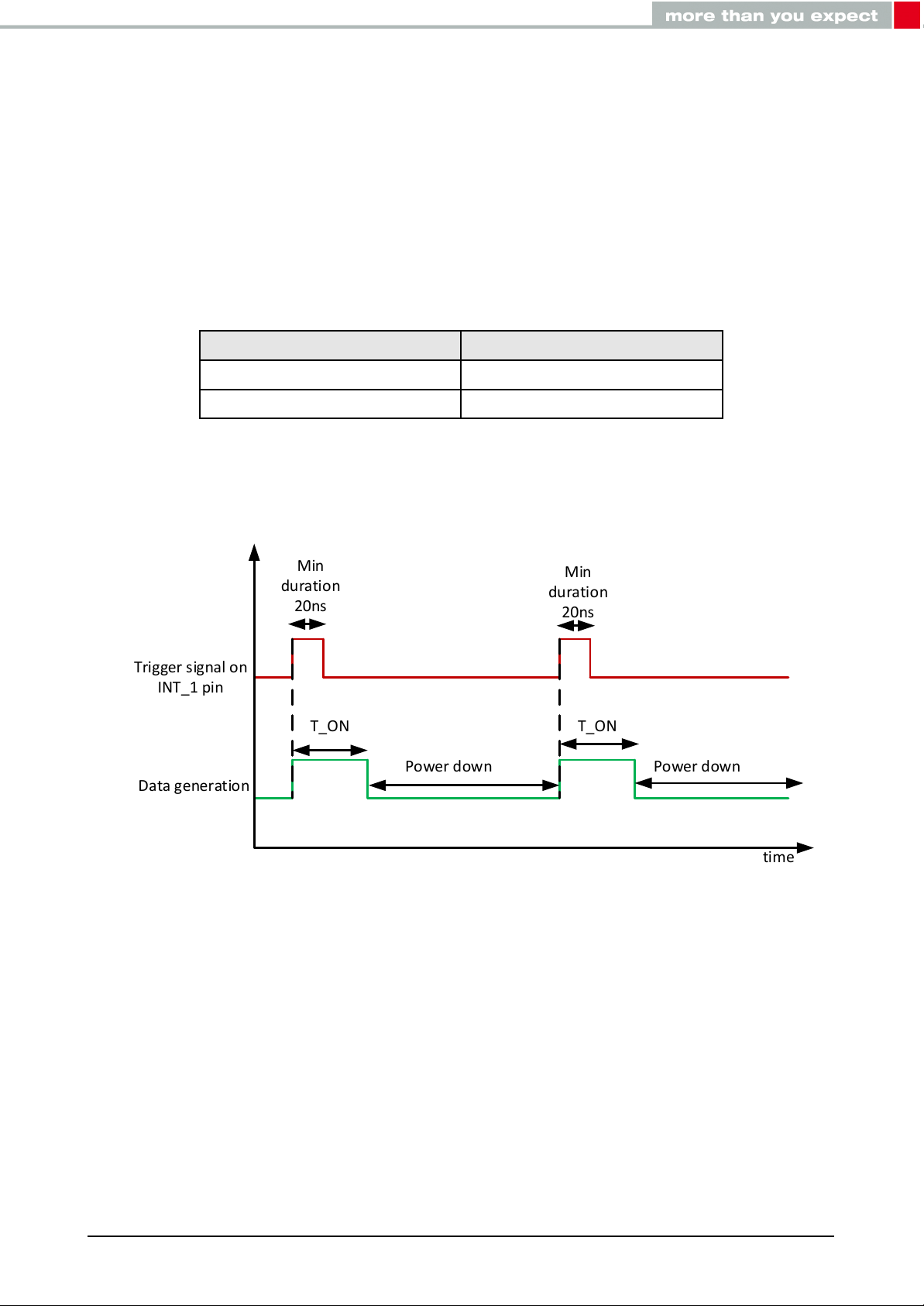
INT_0 pin by writing ’1’ to INT0_DRDY bit in the register CTRL_4 . The minimum duration of
Data generation
Trigger signal on
INT_1 pin
T_ON
Power down
T_ON
Power down
time
Min
duration
20ns
Min
duration
20ns
trigger signal high level is 20 ns.
2. Writing SLP_MODE_1 bit to ’1’ in CTRL_3 register
In this configuration, the data generation takes place by enabling SLP_MODE_1 bit in CTR-
L_3 register. In this case the SLP_MODE_SEL should be set to ’1’. The user can detect the
status of the conversion using DRDY bit/signal or SLP_MODE_1 bit. After conversion, the
SLP_MODE_1 bit in CTRL_3 register(0x22) is automatically set to ’0’.
The conversion time (T_ON) in the normal and low power mode is mentioned in table 18.
Operating mode Conversion time (T_ON)
Normal mode 2.30 ms
Low power mode 1.20 ms
Table 18: Conversion time
Figure 18: Single data conversion using an external trigger signal
Acceleration sensor, Part Nr. 2533020201601
User manual version 2.0 © December 2020
www.we-online.com/sensors 34
Page 36
10 Output data rate
The data sampling rate of the sensor is defined by output data rate. After the device is
powered up with one of the three operating modes, the device is in continuous conversion
of data. One of the following output data rates can be selected through the ODR bits in
CTRL_1. In high performance mode the output data rate of the sensor can be configured
between 12.5 Hz and 1600 Hz. In normal/low power mode the output data rate of the sensor
can be configured between 1.6 Hz and 200 Hz.
Output data rate ODR[3:0] High performance mode
0000
0001 12.5 Hz 1.6 Hz
0010
0011
0100
0101
0110
0111 400 Hz 200 Hz
1000 800 Hz 200 Hz
1001 1600 Hz 200 Hz
Table 19: Output data rate
Power down
Normal Mode / Low power
mode
12.5 Hz
25 Hz
50 Hz
100 Hz
200 Hz
Acceleration sensor, Part Nr. 2533020201601
User manual version 2.0 © December 2020
www.we-online.com/sensors 35
Page 37

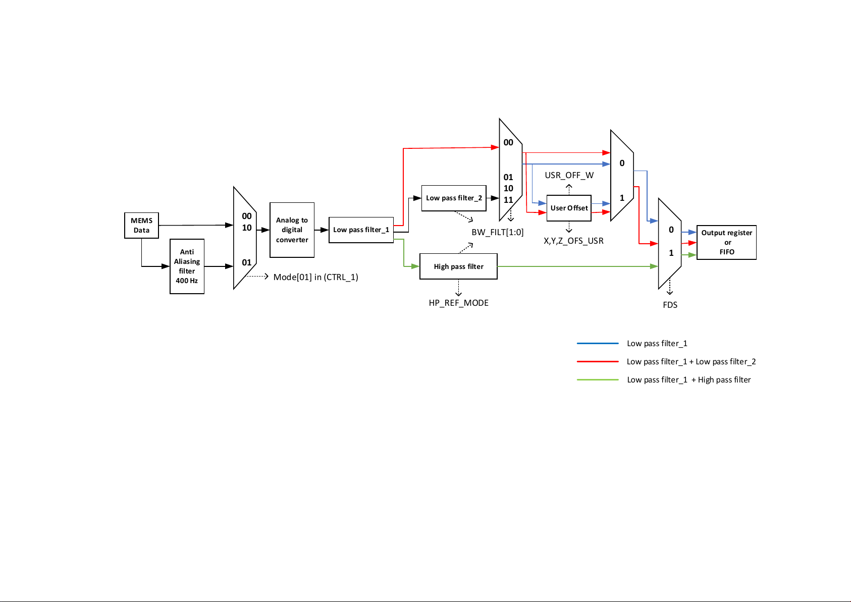
11 Acceleration bandwidth and filtering chain
The acceleration sensor sampling chain consists of a series of blocks from MEMS data to
output register as shown in figure 19.
• MEMS data
• Anti-Aliasing filter
• Analog to digital converter
• Low pass filter 1 and Low pass filter 2
• High pass filter
• User offset
• Output register or FIFO buffer
The output data in the output registers can be generated through three different filtering
paths as shown in the figure 19. The filter setting determines the data path.
The cut-off frequency and number of samples to discard for those three filtering paths are
described in the chapter 11.1, chapter 11.2 and chapter 11.3.The register settings for the
three different data paths are mentioned below.
• Low pass filter _1 (red path)
By setting FDS bit to ’0’ and BW_FILT[1:0] to ’00’ in register CTRL_6
• Low pass filter _1 + Low pass filter _2 (blue path)
By setting FDS bit to ’0’ and BW_FILT[1:0] to ’01’/’10’/’11’ in register CTRL_6
• Low pass filter _1 + High pass filter (green path)
By setting FDS bit to ’1’ in register CTRL_6
Acceleration sensor, Part Nr. 2533020201601
User manual version 2.0 © December 2020
www.we-online.com/sensors 36
Page 38
MEMS
Data
Anti
Aliasing
filter
400 Hz
Analog to
digital
converter
Low pass filter_1
Low pass filter_2
High pass filter
User Offset
Output register
or
FIFO
0
1
FDS
00
10
01
00
01
10
11
0
1
Mode[01] in (CTRL_1)
HP_REF_MODE
BW_FILT[1:0]
USR_OFF_W
X,Y,Z_OFS_USR
Low pass filter_1 + High pass filter
Low pass filter_1 + Low pass filter_2
Low pass filter_1
Figure 19: Block diagram of filtering chain
Page 39
11.1 Low pass filter_1
Mode Output date rate
Samples to discard
BW_FILT[1:0]=00
1
Cutoff (Hz)
Settling@95%
Low power 1.6 Hz to 200 Hz 0 3200
Normal 1.6 Hz to 200 Hz 0 360
High
performance
12.5 Hz to 50 Hz 0 ODR/2
100 Hz to 800 Hz 1 ODR/2
1600 Hz 2 400
Table 20: Low pass filter 1
1
The starting condition of output data rate, operating mode and bandwidth do not impact
the sample values to discard. Turn-on time (first sample available starting from power-down
condition) is 1 / ODR.
11.2 Low pass filter _1 + Low pass filter_2
Mode
Low power
Normal
High
performance
High
performance
High
performance
Output
date rate
1.6 Hz to
200 Hz
1.6 Hz to
200 Hz
12.5 Hz to
100 Hz
200 Hz to
800 Hz
1600 Hz 3 ODR/4 6 ODR/10 12 ODR/20
BW_FILT[1:0]=01 BW_FILT[1:0]=10 BW_FILT[1:0]=11
Samples
to discard
tling@95%
1
Cutoff
Set-
1 ODR/4 5 ODR/10 11 ODR/20
1 ODR/4 5 ODR/10 11 ODR/20
1 ODR/4 5 ODR/10 11 ODR/20
2 ODR/4 5 ODR/10 11 ODR/20
(Hz)
Samples
to discard
Set-
tling@95%
1
Cutoff
(Hz)
Samples
to discard
Set-
tling@95%
1
Cutoff
(Hz)
Table 21: Low pass filter_1 + Low pass filter _2
1
The starting condition of output data rate, operating mode and bandwidth do not impact the
sample values to discard.
Acceleration sensor, Part Nr. 2533020201601
User manual version 2.0 © December 2020
www.we-online.com/sensors 38
Page 40
11.3 Low pass filter _1 + High pass filter
Mode
Low power
Normal
High
performance
High
performance
High
performance
Output
date rate
1.6 Hz to
200 Hz
1.6 Hz to
200 Hz
12.5 Hz to
100 Hz
200 Hz to
800 Hz
1600 Hz 3 ODR/4 6 ODR/10 12 ODR/20
BW_FILT[1:0]=01 or 00 BW_FILT[1:0]=10 BW_FILT[1:0]=11
Samples
to discard
tling@95%
1
Cutoff
Set-
1 ODR/4 5 ODR/10 11 ODR/20
1 ODR/4 5 ODR/10 11 ODR/20
1 ODR/4 5 ODR/10 11 ODR/20
2 ODR/4 5 ODR/10 11 ODR/20
(Hz)
Samples
to discard
Set-
tling@95%
1
Cutoff
(Hz)
Samples
to discard
Set-
tling@95%
1
Cutoff
(Hz)
Table 22: Low pass filter_1 + High pass filter
1
The starting condition of output data rate, operating mode and bandwidth do not impact the
sample values to discard.
11.4 User offset
In order to define user offset for X, Y, and Z axis, the USR_OFF_ON_OUT is set to ’1’
and FDS is set to’0’. User defined offsets are subtracted from the values measured. The
weight of the bits in the offset registers X_OFS_USR, Y_OFS_USR, Z_OFS_USR is defined
through the USR_OFF_W bit in CTRL_7 register.
The offset values are signed values with two’s complement
11.5 High pass filter path
The acceleration sensor includes an embedded high-pass filtering capability to easily remove the DC component of the measured acceleration. As shown in the figure 19, with the
FDS bit in register CTRL_6 the user can route the filter outputs to the output registers.
It is also possible to independently apply the filter to the embedded function data (Free-fall,
wake up, tap detection and etc). This means that it is possible to get filtered data while the
interrupt generation works on unfiltered data.
Acceleration sensor, Part Nr. 2533020201601
User manual version 2.0 © December 2020
www.we-online.com/sensors 39
Page 41
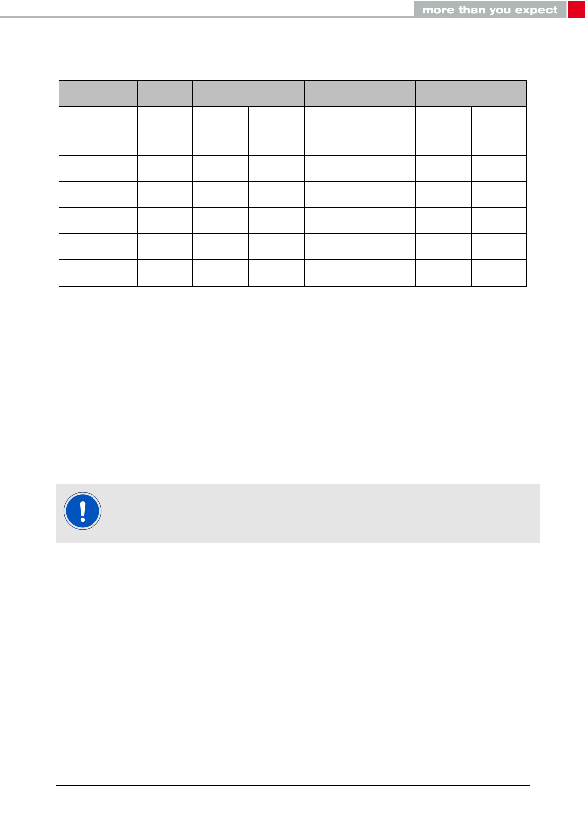
11.5.1 Reference mode
HP enable & REFERENCE disable
Input acceleration
Filtered data
Acceleration
Time
HP enable & REFERENCE enable
Input acceleration
Filtered data
Acceleration
Time
The high-pass filter can be configured in the reference mode. It can be activated using
HP_REF_MODE bit in CTRL_7 register. In this configuration the output data is calculated
as the difference between the input acceleration and the values captured when reference
mode was enabled. In this way only the difference is applied without any filtering.
Figure 20: High pass filter without REFERENCE mode
Figure 21: High pass filter with REFERENCE mode
Acceleration sensor, Part Nr. 2533020201601
User manual version 2.0 © December 2020
www.we-online.com/sensors 40
Page 42

12 First-In First-Out (FIFO) buffer
………………
.
………………
.
………………
.
………………
.
………………
.
………………
.
XL
XH
YL YH ZL ZH
XL(31) XH(31) YL(31) YH(31) ZL(31) ZH(31)
XL(30) XH(30) YL(30) YH(30) ZL(30) ZH (30)
XL(29) XH(29) YL(29) YH(29) ZL(29) ZH(29)
XL(2) XH(2) YL(2) YH(2) ZL(2) ZH(2)
XL(1) XH(1) YL(1) YH(1) ZL(1) ZH (1)
(0x28)
(0x29) (0x2A) (0x2B) (0x2C) (0x2D)
Processor always read the
first sample sets(oldest
sample) stored in the buffer
at the speed of I²C
communication
XL(32) XH(32) YL(32) YH(32) ZL(32) ZH (32)
XL(3) XH(3) YL(3) YH(3) ZL(3) ZH(3)
Buffer filling at the speed of
output data rate
32 level FIFO Buffer
Data In
Data Out
Buffer
The acceleration sensor provides a FIFO (first-in first-out) buffer functionality to prevent continuous communication between the processor and sensor. As a result, it reduces considerable system power consumption. It can store up to 32 output data from all three axis X, Y
and Z. The processor can be notified only when it is necessary to initiate burst read out of
the FIFO buffer content. The interrupt pins INT_0 and/or INT_1 is used to generate interrupt
signals, if the FIFO buffer is full.
The FIFO buffer can be operated using five different modes:
• Bypass mode
• FIFO mode
• Continuous to FIFO mode
• Bypass to Continuous mode
• Continuous mode
Figure 22: First-in First-out Buffer
Acceleration sensor, Part Nr. 2533020201601
User manual version 2.0 © December 2020
www.we-online.com/sensors 41
Page 43

The FIFO buffer stores new data sets in the blocks until all the 32 slots are full. If additional
………………
.
………………
.
………………
.
………………
.
………………
.
………………
.
XL
XH
YL YH ZL ZH
XL XH YL YH ZL ZH
(0x28)
(0x29) (0x2A) (0x2B) (0x2C) (0x2D)
at output data rate
Read through I2C
Communication
FIFO Buffer is
not active
new data is available, the new data replaces the old data in the buffer. The first data enters
the lowest level of the buffer. When the second data is available to be stored in FIFO buffer,
the first data moves one level up and the second data is stored in the lowest level and this
process repeats until the buffer is full. The FIFO buffer can store the data samples with
respect to the selected resolution i.e high performance/normal mode - 14 bits and low power
mode - 12 bits. The rate at which data is stored in the FIFO buffer depends on the selected
output data rate in CTRL_1 register. After enabling the buffer, the output registers (from
0x28 to 0x2D) will get the oldest data sets from the FIFO buffer except for bypass mode.
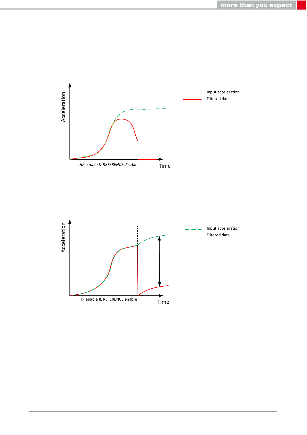
12.1 Bypass mode
In Bypass mode, the generated data is directly available in the output registers. FIFO buffer
is not active in this mode. This mode is activated by writing FMODE[2:0] bits in FIFO_CTRL
register. Bypass mode is also used to clear the content of the FIFO buffer or to reset the
buffer in FIFO mode.
Figure 23: Bypass mode
Acceleration sensor, Part Nr. 2533020201601
User manual version 2.0 © December 2020
www.we-online.com/sensors 42
Page 44

12.2 FIFO mode
………………
.
………………
.
………………
.
………………
.
………………
.
………………
.
XL
XH
YL YH ZL ZH
XL(31) XH(31) YL(31) YH(31) ZL(31) ZH (31)
XL(30) XH(30) YL(30) YH(30) ZL(30) ZH (30)
XL(29) XH(29) YL(29) YH(29) ZL(29) ZH (29)
XL(2) XH(2) YL(2) YH(2) ZL(2) ZH (2)
XL(1) XH(1) YL(1) YH(1) ZL(1) ZH (1)
(0x28)
(0x29) (0x2A) (0x2B) (0x2C) (0x2D)
33rd sample of X, Y, Z
34rd sample of X, Y, Z
35rd sample of X, Y, Z
and so on
Trash
Shift upwards
FIFO_OVG bit = 1
Until
FIFO buffer
read completely
1st sample of X, Y, Z
2nd sample of X, Y, Z
…….
32nd sample of X,Y,Z
XL(3) XH(3) YL(3) YH(3) ZL(3) ZH(3)
XL(32) XH(32) YL(32) YH(32) ZL(32) ZH (32)
In FIFO mode, the 32 levels in FIFO buffer are filled with data samples continuously. When
the buffer is completely filled, the FIFO_OVR bit goes to ’1’, the buffer stops collecting the
data. The FIFO mode is activated by writing ’001’ in FMODE[2:0] field in the FIFO_CTRL
register.
While FIFO buffer starts collecting data, DIFF[5:0] bits in the FIFO_SAMPLES register
changes with respect to the number of samples stored. The speed at which the processor reads the data from the FIFO buffer is not important. Because the data collection is
stopped after the buffer is full and there is no risk that buffer will overwrite the data.
In order to serve the FIFO full (DIFF[5] bit) event as soon as possible, it is recommended to
route the Diff5 bit to the interrupt pin (INT_0 or INT_1) in order to generate an interrupt rather
than FIFO_OVR bit. The difference between the FIFO_OVR bit and Diff5 bit is explained in
figure 25.
When the FIFO mode is enabled, the buffer starts collecting the data at selected output data
rate. The buffer stops collecting the data after the 32 levels are filed i.e. the incoming new
data samples are ignored. The user can read the data from FIFO buffer any time, it is maintained unchanged until the Bypass mode is enabled. The FIFO_OVR bit is reset when the
first sample set has been read by the processor. By enabling the Bypass mode the FIFO
mode will be reset.
Acceleration sensor, Part Nr. 2533020201601
User manual version 2.0 © December 2020
www.we-online.com/sensors 43
Figure 24: FIFO mode
Page 45

…….
FIFO_OVR
FIFO full interrupt
FIFO full
time
FIFO buffer
1
2 3 4 30 31 32
Figure 25: FIFO mode interrupts
12.3 Continuous mode
In continuous mode, the 32 levels of the FIFO buffer is continuously filled and starts to replace new data in the place of old data, when the buffer is full. This process continues until
the processor initiates a read operation to the output registers. When the 32 level buffer is
completely filled, the FIFO_FTH bit goes to ’1’ and it can be routed to interrupt pin which
triggers the processor to read the content of FIFO buffer. This mode can be terminated by
enabling Bypass mode.
The speed at which the processor read the data sets should be faster than
output data rate of the sensor in order to not lose the stored data sets
When a read operation is initiated by the processor to the sensor, the content of the output
registers is moved to the I2C or SPI register. The current oldest FIFO sample is shifted into
the output registers in order to allow the next read operation.
Acceleration sensor, Part Nr. 2533020201601
User manual version 2.0 © December 2020
www.we-online.com/sensors 44
Page 46

………………
.
………………
.
XL XHYL YH ZL
XL(3) XH(3) YL(3) YH(3) ZL(3) ZH(3)
XL(2) XH(2) YL(2) YH(2) ZL(2) ZH(2)
XL(1) XH(1) YL(1) YH(1) ZL(1) ZH(1)
(0x28) (0x29) (0x2A) (0x2B) (0x2C)
(0x2D)
(a read
operation
can be
performed
by processor
at this stage)
………………
.
………………
.
XL
XH
YL YH
ZL ZH
XL(63) XH(63) YL(63) YH(63) ZL(63) ZH(63)
XL(62) XH(62) YL(62) YH(62) ZL(62) ZH(62)
XL(61) XH(61 ) YL(61) YH(61) ZL(61) ZH(61)
(0x28)
(0x29) (0x2A)
(0x2B) (0x2C)
(0x2D)
………………
.
………………
.
………………
.
………………
.
If the processor did not performe the read operation,
buffer will replace old data sets with new data sets
ZH
FIFO_FTH = 1
FIFO_FTH = 1
XL(31) XH(31) YL(31) YH(31) ZL(31) ZH(31)
XL(30) XH(30) YL(30) YH(30) ZL(30) ZH(30)
XL(29) XH(29) YL(29) YH(29) ZL(29) ZH(29)
XL(35) XH(35) YL(35) YH(35) ZL(35) ZH(35)
XL(34) XH(34) YL(34) YH(34) ZL(34) ZH(34)
XL(33) XH(33) YL(33) YH(33) ZL(33) ZH(33)
1,2,3,4…..32 sets 33,34,35….64 sets
………………
.
………………
.
………………
.
………………
.
XL(32) XH(32) YL(32) YH(32) ZL(32) ZH(32) XL(64) XH(64) YL(64) YH(64) ZL(64) ZH(64)
Figure 26: Continuous mode
12.4 Continuous to FIFO mode
In this mode, initially the buffer starts operating in continuous mode and switches to FIFO
mode when the selected interrupt (wake-up. freel-fall, motion, etc) occurs. This mode helps
to collect and analyse the output data samples after an interrupt signal (tap, motion, freefall, etc) is generated. During this mode, the buffer works initially in continuous mode. In
continuous mode, the buffer starts collecting the data samples continuously. As soon as the
activated interrupt signal is generated, the FIFO mode is active and it starts collecting the
output samples until it is full. When the buffer is full, the FIFO_OVG bit is set to ’1’ when the
next samples overwrite the oldest and the FIFO stops collecting the data.
When the selected interrupt occurs, the FIFO mode change is triggered only if
the interrupt signal is routed to INT_0 or INT_1 pin.
The following steps are recommended to enable continuous to FIFO mode.
• Step 1: Enable interrupt features (tap, free-fall, motion and etc)
• Step 2: Route the interrupt signal to either INT_0 or INT_1 pin
• Step 2: Enable the continuous to FIFO mode using FMODE[2:0] in FIFO_CTRL register
Acceleration sensor, Part Nr. 2533020201601
User manual version 2.0 © December 2020
www.we-online.com/sensors 45
Page 47

XH XLYL YH ZL
XL(3) XH(3) YL(3) YH(3) ZL(3) ZH(3)
XL(2) XH(2) YL(2) YH(2) ZL(2) ZH(2)
XL(1) XH(1) YL(1) YH(1) ZL(1) ZH(1)
(0x28) (0x29) (0x2A) (0x2B) (0x2C)
(0x2D)
Interrupt
signal
generated
in INT_0 or
INT_1
………………
XL
XH
YL YH
ZL ZH
XL(35) XH(35) YL(35) YH(35) ZL(35) ZH(35)
XL(34) XH(34 ) YL(34) YH(34) ZL(34) ZH(34)
XL(33) XH(33) YL(33) YH(33) ZL(33) ZH(33)
XL(32) XH(32 ) YL(32) YH(32) ZL(32) ZH(32)
XL(5) XH(5) YL(5) YH(5) ZL(5) ZH(5)
XL(4) XH(4) YL(4) YH(4) ZL(4) ZH(4)
(0x28)
(0x29) (0x2A)
(0x2B) (0x2C)
(0x2D)
The buffer switches to FIFO mode and
starts filling the samples until it is full
ZH
FIFO_OVG = 1
Continuous mode
FIFO mode
Read
operation
by
processor
1
2
3
………………
………………
………………
………………
………………
………………
………………
………………
………………
………………
………………
Figure 27: Continuous to FIFO mode
12.5 Bypass to continuous mode
In this mode, initially the buffer works in bypass mode and as soon as the selected interrupt
signal is generated the buffer switches to continuous mode.
The following steps are recommended to enable Bypass to Continuous mode.
• Step 1: Enable interrupt features (tap, free-fall, motion and etc)
• Step 1: Set FTH[4:0] to 31
• Step 2: Route the interrupt signal to either INT_0 or INT_1 pin
• Step 2: Enable the Continuous to FIFO mode using FMODE[2:0] in FIFO_CTRL register
Initially the buffer works in Bypass mode, so no data is stored in the buffer. When a selected
interrupt signal is generated, the buffer switches to continuous mode and starts to fill the data at selected output data rate. When the programmed threshold is reached, the FIFO_FTH
interrupt goes high, and the processor can start reading all FIFO samples (32 * 6 bytes) as
soon as possible to avoid loss of data. If the FIFO_OVG bit was set, it will change to ’0’,
when the first FIFO data is read creating space for new data.
Acceleration sensor, Part Nr. 2533020201601
User manual version 2.0 © December 2020
www.we-online.com/sensors 46
Page 48
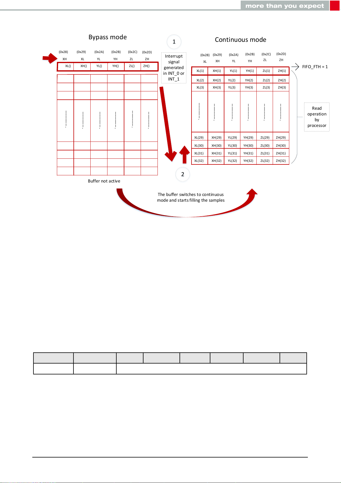
………………
.
………………
.
XL XHYL YH ZL
XL() XH() YL() YH() ZL() ZH()
(0x28) (0x29) (0x2A) (0x2B) (0x2C)
(0x2D)
Interrupt
signal
generated
in INT_0 or
INT_1
………………
.
………………
.
XL
XH
YL YH
ZL ZH
XL(31) XH(31) YL(31) YH(31) ZL(31) ZH(31)
XL(30) XH(30) YL(30) YH(30) ZL(30) ZH(30)
XL(29) XH(29 ) YL(29) YH(29) ZL(29) ZH(29)
XL(1) XH(1) YL(1) YH(1) ZL(1) ZH(1)
(0x28)
(0x29) (0x2A)
(0x2B) (0x2C)
(0x2D)
………………
.
………………
.
………………
.
………………
.
The buffer switches to continuous
mode and starts filling the samples
ZH
FIFO_FTH = 1
Bypass mode
Continuous mode
Read
operation
by
processor
1
2
XL(2) XH(2) YL(2) YH(2) ZL(2) ZH(2)
XL(3) XH(3) YL(3) YH(3) ZL(3) ZH(3)
XL(32) XH(32) YL(32) YH(32) ZL(32) ZH(32)
Buffer not active
………………
.
………………
.
………………
.
………………
.
Figure 28: Bypass to Continuous mode
If the processor does not initiate read operation, the buffer starts replacing old data with new
data. This process will continue until the generated interrupt flag is cleared or buffer goes to
Bypass mode, then the buffer stops collecting the data.
12.6 Understanding FIFO samples and interrupts
12.6.1 FIFO samples
The samples are stored in the buffer at the rate of selected output data rate. The threshold
values are defined using the FIFO_SAMPLES register.
Bit 7 Bit 6 Bit 5 Bit 4 Bit 3 Bit 2 Bit 1 Bit 0
FIFO_FTH FIFO_OVR
• FIFO_FTH bit is used to notify whether the FIFO content is greater than or equal to
the watermark level defined by DIFF[5:0]. This signal can be routed to either INT_0 or
INT_1 pin.
Table 23: FIFO_Samples register
DIFF[5:0]
Acceleration sensor, Part Nr. 2533020201601
User manual version 2.0 © December 2020
www.we-online.com/sensors 47
Page 49

• FIFO_OVR bit defines whether the 32 level buffer is full or not. It can be used to notify
the processor to read whole content of the buffer. When the processor starts reading
the first sample in the buffer, this bit is set to ’0’.
• DIFF[5:0] gives the information about number of levels in the buffer filled with data
samples or number of samples in the buffer read by processor( ’000000b’ for FIFO
empty and ’100000b’ for FIFO is full). This signal also be routed to either INT_0 or
INT_1
12.6.2 FIFO interrupts
12.6.2.1 FIFO threshold (FIFO_FTH bit)
The FIFO threshold is a configurable feature which can be used to produce a specific interrupt, to know whether the FIFO buffer contains at least the number of samples defined
as the threshold level. The user can select the desired level in a range from 0 to 31 using
the FTH[4:0] bits in the FIFO_CTRL register. If the number of entries in FIFO (Diff[5:0]) is
greater than or equal to the value programmed in FTH[4:0], the FIFO_FTH bit is set high
in the FIFO_SAMPLES register. Diff[5:0] increases by one step at the ODR frequency and
decreases by one step every time that a sample reading is performed by the host controller.
12.6.2.2 FIFO full (Diff5 bit)
When the buffer is full, the sensor can be configured to generate an interrupt signal using
Diff5 bit. In order to perform this, set the INT0_DIFF5 bit in the CTRL_4 register to ’1’ or
INT1_DIFF5 bit in the CTRL_5 register to ’1’. To avoid losing samples, the FIFO reading
operation must start and complete inside 1 ODR window.
12.6.2.3 FIFO overrun (FIFO_OVR)
It is possible to configure the device to generate an interrupt using FIFO_OVR, if the overrun
event occurs in FIFO buffer. In order to initiate this, set the INT1_OVR bit of the CTRL_5
register to ’1’.
12.7 How to read data from FIFO Buffer
When any of the operating FIFO buffer mode is selected except Bypass mode, the first sample stored in the buffer is always read from the output registers. After reading the output data
registers, the FIFO blocks are moved one level up vertically to allocate space to store new
samples. The whole content of the FIFO buffer i.e. 32 level of 6 bytes (total of 192 bytes) of
data samples from X_L, X_H, Y_L, Y_H, Z_L and Z_H can be read at once. The content of
the FIFO buffer will be the same even after reading the data and it will be replaced only when
new set of samples stored in FIFO buffer. When the processor initiates a read operation to
the output register 0x28, the automatic increment of the address 0x29, 0x2A, 0x2B, 0x2C
and 0x2D will be performed, if the IF_ADD_INC bit is enabled in CTRL_2 register.
The standard I2C communication protocol has two clock frequencies, standard mode of 100
kHz and full speed mode of 400 kHz clock. In order to perform read operation, the I2C communication takes 29 clock signals to initiate read operation for a specific register. It starts
Acceleration sensor, Part Nr. 2533020201601
User manual version 2.0 © December 2020
www.we-online.com/sensors 48
Page 50

with a start condition + slave address + write register + read register. Additionally, to read
every byte (8 bit register value) 9 clock pulses are necessary. In total 83 clock pulses are
used to read a one sample set from the output registers of X, Y and Z axis (0x28, 0x29,
0x2A, 0x2B, 0x2C and 0x2D). In order to read single sample set from output register it takes
83 pulses * 1/100 kHz (830 µs). To read the whole content of the buffer, a total of 17.57 ms
(29 +9 * 192) time is necessary.
In order to not lose samples, the application should read samples before the FIFO becomes
full, setting a threshold and using the FTH interrupt.
Output data rate (Hz) FTH_TH (I2C - 100 kHz) FTH_TH (I2C - 400 kHz)
50 32 32
100 17 32
200 8 32
400 4 17
800 1 8
1600 - 4
Table 24: Threshold function
Acceleration sensor, Part Nr. 2533020201601
User manual version 2.0 © December 2020
www.we-online.com/sensors 49
Page 51

13 Interrupt pin and functionality
The two independent interrupt pins INT_0 and INT_1 of the sensor can be used to route the
following signals.
• Motion detection interrupt signal
• DRDY signal
• FIFO notification signal
13.1 INT_0 and INT_1
All the motion detection interrupt signals can be routed to the physical interrupt (either INT_0
or INT_1) pins by writing ’1’ to INTERRUPTS_ENABLE bit in CTRL_7 register, otherwise it
can be identified by reading their corresponding status or source register. By default, the
bits in the control registers (CTRL_4 and CTRL_5) are disabled i.e ’0’. Any specific motion
detection interrupt signals can be routed to the physical interrupt pins by enabling the following bits in the registers CTRL_4 and CTRL_5.
Bit 7 Bit 6 Bit 5 Bit 4 Bit 3 Bit 2 Bit 1 Bit 0
INT0_
INT0_6D
• INT0_6D:
• INT0_SINGLE_TAP:
• INT0_WU: :
• INT0_FF:
• INT0_TAP:
• INT0_DIFF5:
• INT0_FTH:
• INT0_DRDY:
Bit 7 Bit 6 Bit 5 Bit 4 Bit 3 Bit 2 Bit 1 Bit 0
INT1_
SLEEP_
STATE
SINGLE
_TAP
INT1_
SLEEP_
CHG
INT0_
WU
6D orientation event detect is routed to the INT_0 pin
Single-tap event detect is routed to the INT_0 pin
Wakeup event detect is routed to the INT_0 pin
Free-fall event detect is routed to the INT_0 pin
Double-tap event detect is routed to the INT_0 pin
FIFO full event is routed to the INT_0 pin
FIFO threshold event is routed to the INT_0 pin
DRDY is routed to the INT_0 pin
INT1_
BOOT
INT0_
FF
Table 25: CTRL_4
INT1_
DRDY
_T
INT0_
TAP
INT1_
OVR
INT0_
DIFF5
INT1_
DIFF5
INT0_
FTH
INT1_
FTH
INT1_
DRDY
INT1_
DRDY
Table 26: CTRL_5
Acceleration sensor, Part Nr. 2533020201601
User manual version 2.0 © December 2020
www.we-online.com/sensors 50
Page 52
• INT1_SLEEP_STATE:
X Y Z X Y Z
Data
DRDY
Data read
Data available Data available
SLEEP_STATE enable is routed to the INT_1 pin
• INT1_SLEEP_CHG:
• INT1_BOOT:
• INT1_DRDY_T:
• INT1_OVR:
• INT1_DIFF5:
• INT1_FTH:
• INT1_DRDY:
Sleep change status is routed to the INT1 pin
Boot state is routed to the INT_1 pin
Temperature DRDY is routed to the INT_1 pin
FIFO overrun interrupt is routed to the INT_1 pin
FIFO full detect is routed to the INT_1 pin
FIFO threshold event is routed to the INT_1 pin
Acceleration DRDY is routed to the INT_1 pin
There is a possibility that more than one interrupt signal is routed to the same interrupt pin.
In that case, a logic level OR combination of the selected interrupt signal is generated. To
know which motion detection event has triggered the interrupt signal, the respective status
register has to be read. After reading the status register, the generated bit in the status
register will be cleared.
13.2 Data ready - DRDY
The DRDY bit status can either be read from STATUS register (0x27) or can be routed
directly to interrupt pins. When new data is generated the DRDY bit is set to ’1’ and it is
set to ’0’ when no data is generated. This DRDY signal can be routed to INT_0 interrupt
pin by enabling the INT0_DRDY bit in CTRL_4 register or to INT_1 interrupt pin by enabling
INT1_DRDY bit in CTRL_5 register. If any of the output channel registers (0x29, 0x2B, 0x2D)
are read, the DRDY signal goes LOW.
Figure 29: DRDY signal
Acceleration sensor, Part Nr. 2533020201601
User manual version 2.0 © December 2020
www.we-online.com/sensors 51
Page 53

14 Application specific sensor features
14.1 Single tap/Double tap
The single tap event interrupt is generated when the applied tap acceleration to any axis is
greater than defined threshold and returns below within specific interval time. Similarly in
double tap event an interrupt is generated, if two consecutive tap acceleration applied to any
axis is greater than the threshold with duration time after first tap acceleration.
14.2 Activity/Inactivity
The activity/inactivity function monitors the sensor, which defines whether the sensor is active or not. This function allows to develop application with low power consumption. If the
sensor is not active, the output data rate automatically goes to output data rate of 12.5 Hz
with low power operating mode. As soon as the sensor detects an activity, the output data
rate is switched back to the selected output data rate.
14.3 Stationary/Motion
Stationary/motion function is similar to the activity/inactivity function but the output data rate
and operating mode will not change after the motion is detected.
14.4 6D Orientation
Six dimension (6D) orientation of the sensor is detected when one axis exceeds a selected threshold and the acceleration values from other two axes are lower than the defined
threshold value.
14.5 Wake-Up
If a number of data samples exceed the defined threshold on both positive and negative
acceleration a wake-up interrupt signal is generated. It can either be achieved by setting
high-pass filter or user defined offset function.
14.6 Free-Fall
Free fall detection interrupt is generated when the device is in free-fall i.e. the acceleration
measured in all axes goes to zero. In a real case, a free-fall zone is defined around the zerog level where all the acceleration values from the three axes are small enough to generate
the interrupt.
For more information about the sensor features refer to the application notes.
Acceleration sensor, Part Nr. 2533020201601
User manual version 2.0 © December 2020
www.we-online.com/sensors 52
Page 54
15 Self test
The acceleration sensor includes a self test feature which tests the sensor functionality without any external force. When the self test feature is enabled, an actuation force is applied
to the sensor which causes the non-stationary part to move. This change in the movement
provides the change in the DC level of the sensor.
The self test function is enabled by writing ’01’ to ST[7:6] in CTRL_3 register which causes
movement in positive direction of the axis. Similarly by writing ’10’ to ST[7:6] in CTRL_3
register causes the movement in negative direction of the axis. When the accelerometer self
test functionality is enabled, the sensor output level is given by the algebraic sum of the data
produced by the electrostatic test force and gravity.
The device should be fixed without any movement during self test procedure
The following procedure is recommended for the self test verification. Refer to the block
diagram in the figure30for further details.
• Average five data samples before enabling the self test
• Average five data samples after enabling the self test
• The difference in the absolute value of each axis provides the self test induced DC
acceleration value.
• Verify the value, whether it is in the range of 70 mg to 1500 mg
Acceleration sensor, Part Nr. 2533020201601
User manual version 2.0 © December 2020
www.we-online.com/sensors 53
Page 55
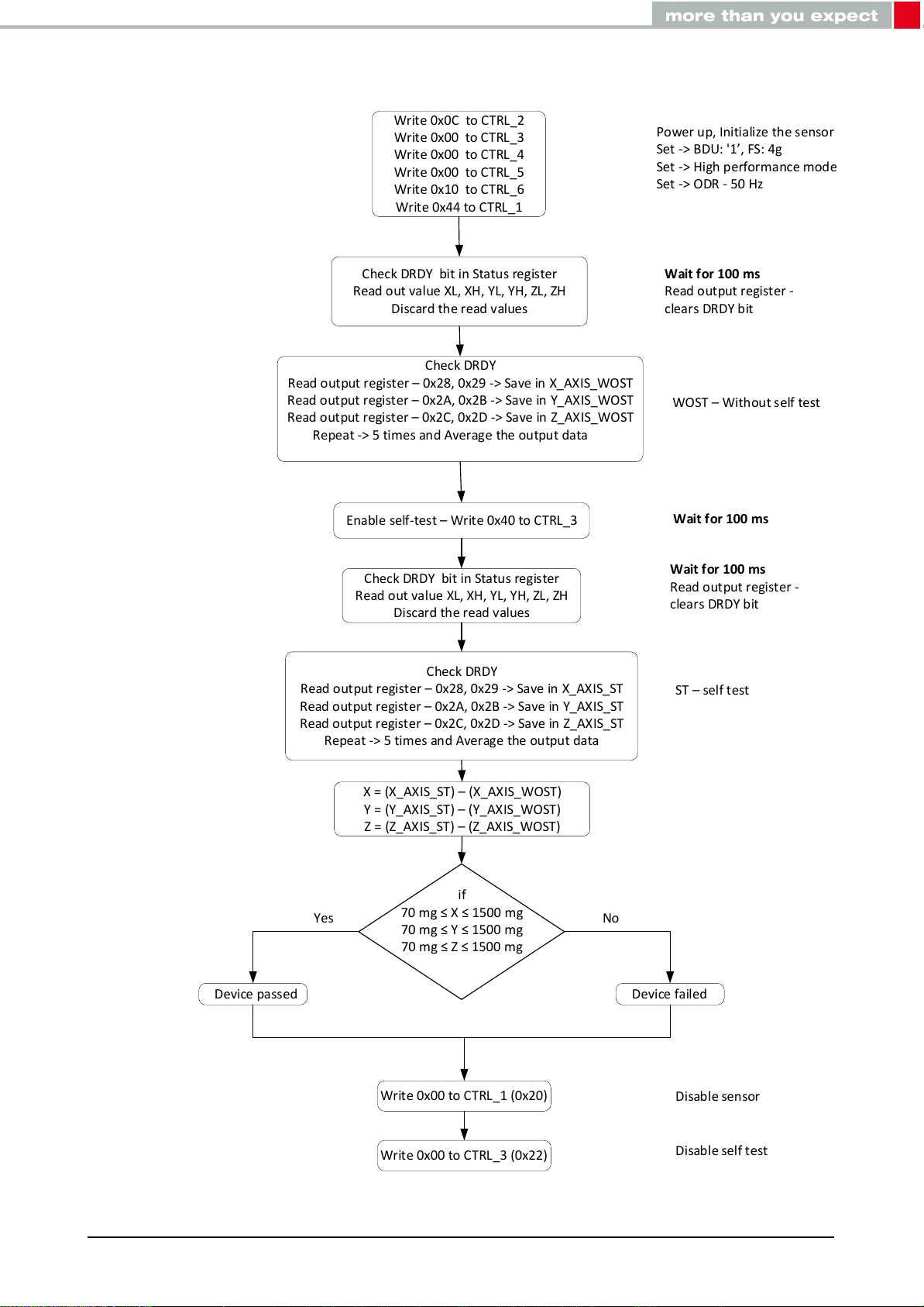
Write 0x0C to CTRL_2
Write 0x00 to CTRL_3
Write 0x00 to CTRL_4
Write 0x00 to CTRL_5
Write 0x10 to CTRL_6
Write 0x44 to CTRL_1
Check DRDY bit in Status register
Read out value XL, XH, YL, YH, ZL, ZH
Discard the read values
Check DRDY
Read output register – 0x28, 0x29 -> Save in X_AXIS_WOST
Read output register – 0x2A, 0x2B -> Save in Y_AXIS_WOST
Read output register – 0x2C, 0x2D -> Save in Z_AXIS_WOST
Repeat -> 5 times and Average the output data
Check DRDY bit in Status register
Read out value XL, XH, YL, YH, ZL, ZH
Discard the read values
X = (X_AXIS_ST) – (X_AXIS_WOST)
Y = (Y_AXIS_ST) – (Y_AXIS_WOST)
Z = (Z_AXIS_ST) – (Z_AXIS_WOST)
if
70 mg ≤ X ≤ 1500 mg
70 mg ≤ Y ≤ 1500 mg
70 mg ≤ Z ≤ 1500 mg
Device passed Device failed
Write 0x00 to CTRL_1 (0x20)
Write 0x00 to CTRL_3 (0x22)
Power up, Initialize the sensor
Set -> BDU: '1’, FS: 4g
Set -> High performance mode
Set -> ODR - 50 Hz
Wait for 100 ms
Enable self-test – Write 0x40 to CTRL_3
Wait for 100 ms
Read output register -
clears DRDY bit
Wait for 100 ms
Read output register -
clears DRDY bit
ST – self test
Check DRDY
Read output register – 0x28, 0x29 -> Save in X_AXIS_ST
Read output register – 0x2A, 0x2B -> Save in Y_AXIS_ST
Read output register – 0x2C, 0x2D -> Save in Z_AXIS_ST
Repeat -> 5 times and Average the output data
Yes No
Disable sensor
Disable self test
WOST – Without self test
Figure 30: Self test procedure
Acceleration sensor, Part Nr. 2533020201601
User manual version 2.0 © December 2020
www.we-online.com/sensors 54
Page 56

16 Sensor output data
16.1 Acceleration sensor
The acceleration output data is obtained by reading output registers (0x28, 0x29, 0x2A,
0x2B, 0x2C and 0x2D). The 8-bit output data from the registers of least significant bit and
most significant bit are concatenated to get 16-bit data for each axis i.e. X, Y and Z axis.
The acceleration data is represented as 16-bit value, left aligned and provided in two’s complement. The value is multiplied with respective sensitivity parameter to convert the data
related to the value in mg.
Below is an example of how to convert the output data into acceleration value in mg. With an
assumption of sensor operating in high performance mode with full scale selection of ±16g.
Step 1:
Read the output registers.
1. X_OUT_L (0x28)
2. X_OUT_H (0x29)
3. Y_OUT_L (0x2A)
4. Y_OUT_H (0x2B)
5. Z_OUT_L (0x2C)
6. Z_OUT_H (0x2D)
Step 2:
Concatenation of two 8-bit output values from the registers to get a 16-bit output value for
each axis.
1. X_16 = X_OUT_H & X_OUT_L
2. Y_16 = Y_OUT_H & Y_OUT_L
3. Z_16 = Z_OUT_H & Z_OUT_L
Acceleration sensor, Part Nr. 2533020201601
User manual version 2.0 © December 2020
www.we-online.com/sensors 55
Page 57
Step 3:
Right shift the output data by 2 bits for high performance mode which provides 14-bit output
data. In case of low power mode enabled, the sensor provides 12-bit data so right shift the
data by 4 bits.
1. X_shift = X_16>>2
2. Y_shift = Y_16>>2
3. Z_shift = Z_16>>2
Step 4:
Multiply with respective sensitivity will provide the acceleration value in mg.
(Sensitivity = 1.952 for FS: ±16g, please refer to table 3)
1. X axis = X_shift * (1.952) = value in mg
2. Y axis = Y_shift * (1.952) = value in mg
3. Z axis = Z_shift * (1.952) = value in mg
Acceleration sensor, Part Nr. 2533020201601
User manual version 2.0 © December 2020
www.we-online.com/sensors 56
Page 58

16.2 Temperature sensor
The acceleration sensor includes embedded temperature sensor for ambient temperature
measurement. The temperature data is represented as a 12 bit in two’s complement form
and left aligned in the output registers T_OUT_L (0x0D) and T_OUT_H (0x0E). Similarly the
temperature data is also represented as a 8 bit output data in two’s complement form in the
output register T_OUT (0x26).
Parameter
Temperature
refresh rate
We recommend our WSEN-TIDS temperature sensor for high accurate and
precise temperature measurements.
Symbol
Test condition
High performance mode for
all ODRs / Normal Mode &
Low power mode for ODRs
equal to 200/100/50 Hz
Normal mode & Low power
mode at ODR - 25 Hz
Normal mode & Low power
mode at ODR - 12.5 Hz
Normal mode & Low power
mode at ODR - 1.6 Hz
Table 27: Temperature refresh rate
Min. Typ. Max. Unit
50 Hz
25
12.5
1.6
16.2.1 12-bit temperature sensor output
To get the 12 bit temperature value from the output registers T_OUT_L (0x0D) and T_OUT_H
(0x0E), first concatenate the OUT_T_L (0x0D) and the OUT_T_H (0x0E) register (16 bits)
i.e. temperature = 0x0E & 0x0D. Then consider only the first 12 bits, converting to the decimal value using 2’s complement, divide for the sensitivity of 16 LSB/°C and finally sum it
with 25°C.
Example code:
float_t temp_to_celsius (int16_t temperature)
{
return (((float_t)temperature / 16.0) + 25.0);
}
Acceleration sensor, Part Nr. 2533020201601
User manual version 2.0 © December 2020
www.we-online.com/sensors 57
Page 59

16.2.2 8-bit temperature sensor output
The interpretation of temperature value from the output register T_OUT (0x26) value is calculated from the look up table (see table 28). The values listed in the table are provided
under the hypothesis of perfect device calibration with no offset or error.
Temperature values T_Out (0x26)
-45°C 0xB9
-44°C 0xBA
-43°C 0xBB
. .
. .
. .
. .
. .
19°C 0xFA
20°C 0xFB
21°C 0xFC
22°C 0xFD
23°C 0xFE
24°C 0xFF
25°C 0x00
26°C 0x01
27°C 0x02
28°C 0x03
29°C 0x04
30°C 0x05
31°C 0x06
. .
. .
. .
. .
. .
83°C 0x3A
84°C 0x3B
85°C 0x3C
Table 28: Temperature look up table
Acceleration sensor, Part Nr. 2533020201601
User manual version 2.0 © December 2020
www.we-online.com/sensors 58
Page 60

17 Register mapping
Register
Addr
(Hex)
0x0D
0x0E
0x0F
0x10-1F
0x20
0x21
0x22
0x23
0x24
0x25
0x26
0x27
0x28
0x29
0x2A
0x2B
0x2C
0x2D
0x2E
0x2F
0x30
0x31
0x32
0x33
0x34
0x35
0x36
0x37
0x38
0x39
0x3A
0x3B
0x3C
0x3D
0x3E
0x3F
Name Bit 7 Bit 6 Bit 5 Bit 4 Bit 3 Bit 2 Bit 1 Bit 0 Type Comments
T_OUT_L TEMP[3:0] 0 0 0 0 R Temperature data registers
T_OUT_H TEMP[7:0] R
DEVICE_ID 0 1 0 0 0 1 0 0 R Device address
1
Reserved
CTRL_1 ODR[3:0] MODE[1:0] LP_MODE[1:0] R/W Control registers
CTRL_2 BOOT SOFT_RESET 0 CS_PU_DISC BDU IF_ADD_INC I2C_DISABLE 0 R/W
CTRL_3 ST[1:0] PP_OD LIR H_LACTIVE 0 SLP_MODE_SEL SLP_MODE_1 R/W
CTRL_4 INT0_6D INT0_SINGLE_TAP INT0_WU INT0_FF INT0_TAP INT0_DIFF5 INT0_FTH INT0_DRDY R/W
CTRL_5 INT1_SLEEP_STATE INT1_SLEEP_CHG INT1_BOOT INT1_DRDY_T INT1_OVR INT1_DIFF5 INT1_FTH INT1_DRDY R/W
CTRL_6 BW_FILT[1:0] FS[1:0] FDS LOW_NOISE 0 0 R/W
T_OUT TEMP[7:0] R Temperature data register
STATUS FIFO_THS WU_IA SLEEP_STATE DOUBLE_TAP SINGLE_TAP 6D_IA FF_IA DRDY R Status data register
X_OUT_L X_L[3:0] X_L[1:0]
X_OUT_H X_H[7:0] R
Y_OUT_L Y_L[3:0] Y_L[1:0]
Y_OUT_H Y_H[7:0] R
Z_OUT_L Z_L[3:0] Z_L[1:0]
Z_OUT_H Z_H[7:0] R
FIFO_CTRL FMODE[2:0] FTH[4:0] R/W FIFO Control register
FIFO_SAMPLES FIFO_FTH FIFO_OVR DIFF[5:0] R Unread samples stored in FIFO
TAP_X_TH 4D_EN 6D_TH[1:0] TAP_X_TH[4:0] R/W Tap thresholds
TAP_Y_TH TAP_PRIOR[2:0] TAP_Y_TH[4:0] R/W
TAP_Z_TH TAP_X_EN TAP_Y_EN TAP_Z_EN TAP_Z_TH[4:0] R/W
INT_DUR LATENCY[3:0] QUIET[1:0] SHOCK[1:0] R/W Interrupt duration
WAKE_UP_TH SINGLE_DOUBLE_TAP SLEEP_ON WK_TH[5:0] R/W Wake up threshold
WAKE_UP_DUR FF_DUR5 WAKE_DUR[1:0] STATIONARY SLEEP_DUR[3:0] R/W Wake up duration
FREE_FALL FF_DUR[4:0] FF_TH[2:0] R/W Free fall configuration
STATUS_DETECT OVR DRDY_T SLEEP_STATE_IA DOUBLE_TAP SINGLE_TAP 6D_IA FF_IA DRDY R Status register
WAKE_UP_EVENT 0 0 FF_IA SLEEP_STATE IA WU_IA X_WU Y_WU Z_WU R Wake up event
TAP_EVENT 0 TAP_IA SINGLE_TAP DOUBLE_TAP TAP_SIGN X_TAP Y_TAP Z_TAP R Tap event
6D_EVENT 0 6D_IA ZH ZL YH YL XH XL R 6D event
ALL_INT_EVENT 0 0 SLEEP_CHANGE_IA 6D_IA DOUBLE_TAP SINGLE_TAP WU_IA FF_IA R
X_OFS_USR X_OFS_USR[7:0] R/W
Y_OFS_USR Y_OFS_USR[7:0] R/W
Z_OFS_USR Z_OFS_USR[7:0] R/W
CTRL_7 DRDY_PULSED INT1_ON_INT0 INTERRUPTS_ENABLE USR_OFF_ON_OUT USR_OFF_ON_WU USR_OFF_W HP_REF_MODE LPASS_ON6D R/W
- - Reserved
2
2
2
0 0 R Acceleration data registers
0 0 R
0 0 R
Page 61

1
The registers contents that are loaded at boot procedure should not be changed. They
contain the factory calibration values and their content is automatically restored when the
device is powered up.
Writing to Reserved registers(0x10 - 0x1F) is not allowed, it will cause permanent damage to the sensor
2
If Low power mode is enabled this bit is set to ’0’
18 Register description
18.1 T_OUT_L (0x0D)
The value of the temperature output registers T_OUT_L(0x0D) and T_OUT_H(0x0E) is expressed in 12-bit resolution. Please refer chapter 15.2.1 to obtain the temperature value
from 12-bit value of the output registers.
Bit 7 Bit 6 Bit 5 Bit 4 Bit 3 Bit 2 Bit 1 Bit 0 Type
TEMP[3:0]
Table 29: T_OUT_L register
bits Description
4 least significant bits (LSB) of the temperature sensor output. Sensitivity =
TEMP[3:0]
1/16°C/LSB. T_OUT_L (0x0D) together with T_OUT_H (0x0E) forms the
value expressed as 16 bit word in 2’s complement
Table 30: T_OUT_L register description
0 0 0 0 R
18.2 T_OUT_H (0x0E)
Bit 7 Bit 6 Bit 5 Bit 4 Bit 3 Bit 2 Bit 1 Bit 0 Type
TEMP[7:0]
R
Table 31: T_OUT_H register
Acceleration sensor, Part Nr. 2533020201601
User manual version 2.0 © December 2020
www.we-online.com/sensors 60
Page 62

bits Description
8 most significant bits (MSB) of the temperature sensor output. Sensitivity
TEMP[7:0]
= 1/16°C/LSB. T_OUT_L (0x0D) together with T_OUT_H (0x0E) forms the
value expressed as 16 bit word in 2’s complement
Table 32: T_OUT_H register description
18.3 Device_ID (0x0F)
The value of this register gives the device ID, a value which is fixed: 0x44(b01000100).
Bit 7 Bit 6 Bit 5 Bit 4 Bit 3 Bit 2 Bit 1 Bit 0 Type
0 1 0 0 0 1 0 0 R
Table 33: Device_ID register
18.4 CTRL_1 (0x20)
Bit 7 Bit 6 Bit 5 Bit 4 Bit 3 Bit 2 Bit 1 Bit 0 Type
ODR[3:0] MODE[1:0] LP_MODE[1:0]
Table 34: CTRL_1 register
ODR[3:0] is used to select the operating mode and output data rate.
ODR[3:0] Power down / data rate configuration
0000 Power down
0001 High performance / Normal mode - 12.5 Hz & Low power mode 1.6 Hz
0010 High performance / Normal mode / Low power mode - 12.5 Hz /
0011 High performance / Normal mode / Low power mode - 25 Hz /
0100 High performance / Normal mode / Low power mode - 50 Hz /
0101 High performance / Normal mode / Low power mode - 100 Hz /
0110 High performance / Normal mode / Low power mode - 200 Hz /
0111 High performance - 400 Hz / Normal mode & Low power mode 200 Hz
1000 High performance - 800 Hz / Normal mode & Low power mode 200 Hz
R/W
1001 High performance - 1600 Hz / Normal mode & Low power mode 200 Hz
Table 35: Output data rate configuration
Acceleration sensor, Part Nr. 2533020201601
User manual version 2.0 © December 2020
www.we-online.com/sensors 61
Page 63

MODE[1:0] Operating mode and resolution
00 Normal mode (14-bit resolution) / Low power mode (12-bit resolution)
01 High performance mode(14-bit resolution)
10 Single data conversion on demand mode (12/14-bit resolution)
11 -
Table 36: Mode selection
LP_MODE[1:0] Operating mode and resolution
00 Low power mode (12-bit resolution)
10 Normal mode (14-bit resolution)
Table 37: Normal and Low power mode selection
18.5 CTRL_2 (0x21)
Bit 7 Bit 6 Bit 5 Bit 4 Bit 3 Bit 2 Bit 1 Bit 0 Type
BOOT
SOFT_
RESET
1
0
CS_PU_
DISC
BDU
IF_ADD
_INC
I2C_
DISABLE
1
0
Table 38: CTRL_2 register
1. this bit must bit set to 0 for proper operation of the sensor.
bits Description
This bit is set to ’1’ during boot sequence, the correct trimming parameters
BOOT
are retrieved from the non-volatile memory into the register. After boot
sequence is completed this bit automatically returns to 0. Default value: 0
(0: disabled, 1: enabled)
SOFT_
RESET
CP_PU_
DISC
BDU
This bit is used to reset all control registers. After reset it is set back to ’0’.
Default value: 0 (0: disabled, 1: enabled)
Disconnect CS pull up. Default value: 0 (0: pull up connected to CS pin, 1:
pull up disconnected to CS pin)
Block data update. Default value: 0 (0: Continuous update, 1: Output
registers are not updated until MSB and LSB read)
R/W
IF_ADD_
INC
I2C_
DISABLE
Register address automatically incremented during multiple byte access
with I2C or SPI interface. Default value 0. (0: disabled, 1: enabled)
Disable I2C communication. Default value: 0 (0: I2C interface enabled, 1: I
interface disabled)
2
Table 39: CTRL_2 register description
Acceleration sensor, Part Nr. 2533020201601
User manual version 2.0 © December 2020
www.we-online.com/sensors 62
Page 64

18.5.1 Block data update (BDU)
It is strongly recommended to set the BDU bit to ’1’ in the CTRL_1 register. By default the
BDU bit is ’0’ and the output registers are continuously updated. When the BDU bit is set
to ’1’ the content of the output registers is not updated until both MSB and LSB are read.
It avoids reading values related to different samples. As soon as the BDU is activated, the
output registers always contain the most recent output data produced by the sensor. If the
processor initiate the read function of a given pair (X_OUT_L and X_OUT_H, Y_OUT_L and
Y_OUT_H, Z_OUT_L and Z_OUT_H), the update for that pair is blocked until both MSB and
LSB of the data are read.
18.6 CTRL_3 (0x22)
Bit 7 Bit 6 Bit 5 Bit 4 Bit 3 Bit 2 Bit 1 Bit 0 Type
ST[1:0]
bits Description
ST[1:0] Self test enable. Defalut value: 00
PP_OD
LIR
H_LACTIVE Interrupt active high, low. Default: 0 (0: active high, 1: active low)
SLP_MODE
_SEL
SLP_MODE
_1
PP_
OD
Push-pull/open-drain selection on interrupt pin. Default: 0 (0: push-pull, 1:
Latched interrupt. Switches between latched (’1’-logic) and pulsed
(’0’-logic) mode for sensor function source signals and the signal routed to
interrupt pins. Default value: 0 (0: Interrupt request not latched, 1: interrupt
Single data conversion on demand selection. 0: enabled by external trigger
signal on INT_1, 1: enabled by writing SLP_MODE_1 to 1 using I2C or SPI.
Single data conversion on demand mode enable. When SLP_MODE_SEL
= ’1’ and this bit is set to ’1’, single data conversion on demand mode
starts. When XL data are available in the registers, this bit is set to ’0’
automatically and the device is ready for another triggered session.
LIR
Table 40: CTRL_3 register
H_
LACTIVE
request latched)
0
open-drain)
SLP_
MODE
_SEL
SLP_
MODE
_1
R/W
Table 41: CTRL_3 register description
Acceleration sensor, Part Nr. 2533020201601
User manual version 2.0 © December 2020
www.we-online.com/sensors 63
Page 65

ST[1:0] Self-test mode
00 Normal mode
01 Positive sign self-test
10 Negative sign self-test
11 -
Table 42: Self-test mode
18.7 CTRL_4 (0x23)
Bit 7 Bit 6 Bit 5 Bit 4 Bit 3 Bit 2 Bit 1 Bit 0 Type
INT0_
6D
bits Description
INT0_6D
INT0_
SINGLE_
TAP
INT0_WU
INT0_FF
INT0_TAP
IN0_
SINGLE
_TAP
Single-tap recognition signal is routed to INT_0 pin. Default value: 0 (0:
Double-tap recognition signal is routed to INT_0 pin. Default value: 0 (0:
INT0
_WU
6D recognition signal is routed to INT_0 pin. Default: 0 (0: disabled, 1:
Wakeup recognition signal is routed to INT_0 pin. Default value: 0 (0:
Free-fall recognition signal is routed to INT_0 pin. Default value: 0 (0:
INT0
_FF
Table 43: CTRL_4 register
INT0
_TAP
enabled)
disabled, 1: enabled)
disabled, 1: enabled)
disabled, 1: enabled)
disabled, 1: enabled)
INT0_
DIFF5
INT0_
FTH
INT0_
DRDY
R/W
INT0_DIFF5
INT0_FTH
INT0_DRDY
Acceleration sensor, Part Nr. 2533020201601
User manual version 2.0 © December 2020
www.we-online.com/sensors 64
FIFO full recognition signal is routed to INT_0 pin. Default value: 0 (0:
disabled, 1: enabled)
FIFO threshold interrupt signal is routed to INT_0 pin. Default value: 0 (0:
disabled, 1: enabled))
Data-Ready interrupt signal is routed to INT_0 pin. Default value: 0 (0:
disabled, 1: enabled)
Table 44: CTRL_4 register description
Page 66

18.8 CTRL_5 (0x24)
Bit 7 Bit 6 Bit 5 Bit 4 Bit 3 Bit 2 Bit 1 Bit 0 Type
INT1_
SLEEP
_STATE
bits Description
INT1_
SLEEP
_STATE
INT1_
SLEEP_
CHG
INT1_BOOT
INT1_DRDY_TTemperature data-ready signal is routed to INT_1 pin. Default value: 0 (0:
INT1_OVR
INT1_
SLEEP_
CHG
Sleep change status signal is routed to INT_1 pin. Default value: 0 (0:
Boot status signal is routed to INT_1 pin. Default value: 0 (0: disabled, 1:
FIFO overrun interrupt signal is routed to INT_1 pin. Default value: 0 (0:
INT1_
BOOT
Sleep state signal is routed to INT_1 pin. Default: 0 (0: disabled, 1:
INT1_
DRDY_T
Table 45: CTRL_5 register
INT1_
OVR
enabled)
disabled, 1: enabled)
enabled)
disabled, 1: enabled)
disabled, 1: enabled)
INT1_
DIFF5
INT1_
FTH
INT1_
DRDY
R/W
INT1_DIFF5
INT1_FTH
INT1_DRDY
FIFO full recognition signal is routed to INT_1 pin. Default value: 0 (0:
disabled, 1: enabled)
FIFO threshold interrupt signal is routed to INT_1 pin. Default value: 0 (0:
disabled, 1: enabled))
Data-Ready interrupt signal is routed to INT_1 pin. Default value: 0 (0:
disabled, 1: enabled)
Table 46: CTRL_5 register description
Acceleration sensor, Part Nr. 2533020201601
User manual version 2.0 © December 2020
www.we-online.com/sensors 65
Page 67
18.9 CTRL_6 (0x25)
Bit 7 Bit 6 Bit 5 Bit 4 Bit 3 Bit 2 Bit 1 Bit 0 Type
BW_FILT[1:0] FS[1:0]
Table 47: CTRL_6 register
bits Description
FDS
LOW_NOISE Low noise configuration (0: disabled, 1: enabled)
BW_FILT[1:0] Bandwidth selection
00 ODR/2 (except for ODR = 1600 Hz, 400 Hz)
01 ODR/4 (High pass / Low pass filter)
10 ODR/10 (High pass / Low pass filter)
11 ODR/20 (High pass / Low pass filter)
Filtered data type selection. Default: 0 (0: low-pass filter path selected, 1:
Table 48: CTRL_6 register description
FDS
high-pass filter path selected)
LOW_
NOISE
0 0 R/W
Table 49: Filtering cut-off selection
FS[1:0] Full scale selection
00 ±2g
01 ±4g
10 ±8g
11 ±16g
Table 50: Full scale selection
18.10 T_OUT (0x26)
Temperature output data in 8-bit resolution.
Bit 7 Bit 6 Bit 5 Bit 4 Bit 3 Bit 2 Bit 1 Bit 0 Type
TEMP[7:0]
R
Table 51: T_OUT register
Acceleration sensor, Part Nr. 2533020201601
User manual version 2.0 © December 2020
www.we-online.com/sensors 66
Page 68

bits Description
Temperature data in 8-bit resolution is expressed as two’s complement sign
TEMP[7:0]
with sensitivity = 1°C/LSB. Please refer the table28for interpretation of
temperature value.
Table 52: T_OUT register description
18.11 STATUS (0x27)
Bit 7 Bit 6 Bit 5 Bit 4 Bit 3 Bit 2 Bit 1 Bit 0 Type
FIFO
_THS
FIFO_THS
WU_IA
SLEEP_
STATE
DOUBLE_
SINGLE_
6D_IA
WU_IA
bits Description
TAP
TAP
SLEEP
_STATE
FIFO threshold status bit (0: FIFO filling is lower than threshold level, 1:
FIFO filling is equal to or higher than the threshold level.))
Wakeup event detection status bit (0: Wakeup event not detected, 1:
Sleep event status bit (0: Sleep event not detected, 1: Sleep event
Double-tap event status bit (0: Double-tap event not detected, 1:
Single-tap event status bit (0: Single-tap event not detected, 1: Single-tap
Source of change in position portrait/landscape/face-up/face-down. (0: no
DOUBLE
_TAP
Table 53: STATUS register
event detected, 1: a change in position detected)
SINGLE
_TAP
Wakeup event detected)
detected)
Double-tap event detected)
event detected)
6D_IA FF_IA DRDY R
FF_IA
DRDY Data-ready status bit (0: not ready, 1: X-, Y- and Z-axis new data available)
Acceleration sensor, Part Nr. 2533020201601
User manual version 2.0 © December 2020
www.we-online.com/sensors 67
Free-fall event detection bit (0: free-fall event not detected; 1: free-fall event
detected)
Table 54: STATUS register
Page 69

18.12 X_OUT_L (0x28)
Bit 7 Bit 6 Bit 5 Bit 4 Bit 3 Bit 2 Bit 1 Bit 0 Type
X_L[3:0] X_L[1:0]
Table 55: X_OUT_L register
bits Description
If low power mode is enabled, the data from this register gives the 4 least
X_L[3:0]
X_L[1:0]
significant bits of X-axis acceleration sensor output. The remaining bits are
zero in the register.
If high performance mode/normal mode is enabled, the data from this
register combined with X_L[3:0] (i.e. X_L[3:0] and X_L[1:0]) gives the 6
least significant bits of X-axis acceleration sensor output. The remaining
bits are zero in the register.
Table 56: X_OUT_L registerr description
1
0 0 R
It gives the 8 least significant bits of X-axis acceleration sensor output. Combined with data
from X_OUT_H(0x29) register, it gives the output value expressed as a 16-bit word in 2’s
complement.
1. If Low power mode 1 is enabled, this bit is set to ’0’.
18.13 X_OUT_H (0x29)
Bit 7 Bit 6 Bit 5 Bit 4 Bit 3 Bit 2 Bit 1 Bit 0 Type
X_H[7:0]
Table 57: X_OUT_H register
It gives the 8 most significant bits of X-axis acceleration sensor output. Combined with data
from X_OUT_L(0x28) register, it gives the output value expressed as a 16-bit word in 2’s
complement.
R
Acceleration sensor, Part Nr. 2533020201601
User manual version 2.0 © December 2020
www.we-online.com/sensors 68
Page 70
18.14 Y_OUT_L (0x2A)
Bit 7 Bit 6 Bit 5 Bit 4 Bit 3 Bit 2 Bit 1 Bit 0 Type
Y_L[3:0] Y_L[1:0]
Table 58: Y_OUT_L register
bits Description
If low power mode is enabled, the data from this register gives the 4 least
Y_L[3:0]
Y_L[1:0]
significant bits of Y-axis acceleration sensor output. The remaining bits are
zero in the register.
If high performance mode/normal mode is enabled, the data from this
register combined with Y_L[3:0] (i.e. Y_L[3:0] and Y_L[1:0]) gives the 6
least significant bits of Y-axis acceleration sensor output. The remaining
bits are zero in the register.
Table 59: Y_OUT_L register description
1
0 0 R
It gives the 8 least significant bits of Y-axis acceleration sensor output. Combined with data
from Y_OUT_H(0x2B) register, it gives the output value expressed as a 16-bit word in 2’s
complement.
1. If Low power mode 1 is enabled, this bit is set to ’0’.
18.15 Y_OUT_H (0x2B)
Bit 7 Bit 6 Bit 5 Bit 4 Bit 3 Bit 2 Bit 1 Bit 0 Type
Y_H[7:0]
Table 60: Y_OUT_H register
It gives the 8 most significant bits of Y-axis acceleration sensor output. Combined with data
from Y_OUT_L(0x2A) register, it gives the output value expressed as a 16-bit word in 2’s
complement.
R
Acceleration sensor, Part Nr. 2533020201601
User manual version 2.0 © December 2020
www.we-online.com/sensors 69
Page 71
18.16 Z_OUT_L (0x2C)
Bit 7 Bit 6 Bit 5 Bit 4 Bit 3 Bit 2 Bit 1 Bit 0 Type
Z_L[3:0] Z_L[1:0]
Table 61: Z_OUT_L register
bits Description
If low power mode is enabled, the data from this register gives the 4 least
Y_L[3:0]
Y_L[1:0]
significant bits of Z-axis acceleration sensor output. The remaining bits are
zero in the register.
If High performance mode/normal mode is enabled, the data from this
register combined with Z_L[3:0] (i.e. Z_L[3:0] and Z_L[1:0]) gives the 6
least significant bits of Z-axis acceleration sensor output. The remaining
bits are zero in the register.
Table 62: Z_OUT_L register description
1
0 0 R
It gives the 8 least significant bits of Z-axis acceleration sensor output. Combined with data
from Z_OUT_H(0x2D) register, it gives the output value expressed as a 16-bit word in 2’s
complement.
1. If Low power mode 1 is enabled, this bit is set to ’0’.
18.17 Z_OUT_H (0x2D)
Bit 7 Bit 6 Bit 5 Bit 4 Bit 3 Bit 2 Bit 1 Bit 0 Type
Z_H[7:0]
Table 63: Z_OUT_H register
It gives the 8 most significant bits of Z-axis acceleration sensor output. Combined with data
from Z_OUT_L(0x2C) register, it gives the output value expressed as a 16-bit word in 2’s
complement.
R
18.18 FIFO_CTRL (0x2E)
Bit 7 Bit 6 Bit 5 Bit 4 Bit 3 Bit 2 Bit 1 Bit 0 Type
FMODE[2:0] FTH[4:0]
Table 64: FIFO_CTRL register
Acceleration sensor, Part Nr. 2533020201601
User manual version 2.0 © December 2020
www.we-online.com/sensors 70
R/W
Page 72
FMODE[2:0] Mode Description
000 Enable Bypass mode and FIFO buffer is turned off(not active)
001 Enable FIFO mode
010 Reserved
011 Enable Continuous to FIFO mode
100 Enable Bypass to Continuous mode
101 Reserved
110 Enable continuous mode
111 Reserved
Table 65: FIFO_CTRL register description
The functionality of the FTH bits are explained in the chapter
12.6.2
18.19 FIFO_SAMPLES (0x2F)
Bit 7 Bit 6 Bit 5 Bit 4 Bit 3 Bit 2 Bit 1 Bit 0 Type
FIFO_FTH FIFO_OVR
Table 66: FIFO_SAMPLES register
bits Description
FIFO_FTH
FIFO_OVR
Diff[5:0]
FIFO threshold status bit. (0: FIFO filling is lower than threshold level, 1:
FIFO filling is equal to or higher than the threshold level)
FIFO overrun status. (0: FIFO is not completely filled, 1: FIFO is
completely filled and at least one sample has been overwritten)
Defines the number of unread samples stored in FIFO. (’000000’ = FIFO
empty, ’100000’ = FIFO full, 32 unread samples)
DIFF[5:0]
R
Table 67: FIFO_SAMPLES register description
18.20 TAP_X_TH (0x30)
Bit 7 Bit 6 Bit 5 Bit 4 Bit 3 Bit 2 Bit 1 Bit 0 Type
4D_EN
Acceleration sensor, Part Nr. 2533020201601
User manual version 2.0 © December 2020
www.we-online.com/sensors 71
6D_TH[1:0] TAP_THSX[4:0]
Table 68: TAP_X_TH register
R/W
Page 73
bits Description
4D detection portrait/landscape position enable. (0: no position
4D_EN
TAP_THSX_[4:0] Threshold for TAP recognition at FS = ±2g on X direction
6D_THS[1:0] Threshold definition (degrees)
00 6 (80 degrees)
01 11(70 degrees)
10 16(60 degrees)
11 21(50 degrees)
detected; 1: portrait/landscape detection and face-up/face-down
position enabled).
Table 69: TAP_X_TH register description
Table 70: 4D/6D threshold setting FS: ±2g description
18.21 TAP_Y_TH (0x31)
Bit 7 Bit 6 Bit 5 Bit 4 Bit 3 Bit 2 Bit 1 Bit 0 Type
TAP_PRIOR[2:0] TAP_THSY[4:0]
Table 71: TAP_Y_TH register
bits Description
TAP_THSY[4:0] Threshold for tap recognition at FS: ±2g on Y direction.
Table 72: TAP_Y_TH register description
TAP_PRIOR[2:0]
000
001
010
011
100
Max Priority Mid Priority Min Priority
X Y Z
Y X Z
X Z Y
Z Y X
X Y Z
R/W
101
110
111
Table 73: Axis priority for tap detection
Acceleration sensor, Part Nr. 2533020201601
User manual version 2.0 © December 2020
www.we-online.com/sensors 72
Y Z X
Z X Y
Z Y X
Page 74

18.22 TAP_Z_TH (0x32)
Bit 7 Bit 6 Bit 5 Bit 4 Bit 3 Bit 2 Bit 1 Bit 0 Type
TAP_X_EN TAP_Y_EN TAP_Z_EN
Table 74: TAP_Z_TH register
bits Description
TAP_X_EN Enables X direction in tap recognition. (0: disabled, 1: enabled)
TAP_Y_EN Enables Y direction in tap recognition. (0: disabled, 1: enabled)
TAP_Z_EN Enables Z direction in tap recognition. (0: disabled, 1: enabled)
TAP_THSZ_[4:0] Threshold for tap recognition at FS: ±2g on Z direction.
Table 75: TAP_Z_TH register description
TAP_THSZ[4:0]
18.23 INT_DUR (0x33)
Bit 7 Bit 6 Bit 5 Bit 4 Bit 3 Bit 2 Bit 1 Bit 0 Type
LATENCY[3:0] QUIET[1:0] SCHOCK[1:0]
R/W
R/W
Table 76: INT_DUR register
bits Description
It defines the maximum duration time gap for double-tap recognition.
When double-tap recognition is enabled, this register expresses the
LATENCY[3:0]
QUIET[1:0]
SHOCK[1:0]
maximum time between two successive detected taps to determine a
double-tap event. Default value is LATENCY[3:0] = 0000 (i.e. 16 *
1/ODR) 1 LSB = 32 * 1/ODR
It defines the expected quiet time after a tap detection. This register
defines the time after the first detected tap in which there must not be
any over-threshold event. Default value is QUIET[1:0] = 00 (i.e. 2 *
1/ODR) 1 LSB = 4 * 1/ODR
It defines the maximum duration of over-threshold event. This register
defines the maximum time of an over-threshold signal detection to be
recognized as a tap event. Default value is SHOCK[1:0] = 00 (i.e. 4 *
1/ODR) 1 LSB = 8 *1/ODR
Table 77: INT_DUR register description
Acceleration sensor, Part Nr. 2533020201601
User manual version 2.0 © December 2020
www.we-online.com/sensors 73
Page 75

18.24 WAKE_UP_TH (0x34)
Bit 7 Bit 6 Bit 5 Bit 4 Bit 3 Bit 2 Bit 1 Bit 0 Type
SINGLE_
DOUBLE _TAP
bits Description
SINGLE_
DOUBLE _TAP
SLEEP_ON
WK_THS[5:0]
SLEEP_ON
Table 78: WAKE_UP_TH register
Enable single/double-tap event. Default value: 0 (0: enable only
single-tap, 1: enable both single and double-tap)
Enables inactivity(sleep). Default value: 0 (0: sleep disabled, 1: sleep
Defines Wakeup threshold, 6-bit unsigned 1 LSB = 1/64 of FS. Default
Table 79: WAKE_UP_TH register description
18.25 WAKE_UP_DUR (0x35)
WK_TH[5:0]
enabled)
value: 000000
R/W
Bit 7 Bit 6 Bit 5 Bit 4 Bit 3 Bit 2 Bit 1 Bit 0 Type
FF_DUR5
bits Description
FF_DUR5
WAKE_DUR[1:0] This bit defines Wakeup duration. 1 LSB = 1 *1/ODR
STATIONARY
SLEEP_DUR[3:0]
WAKE_DUR[1:0]
Table 80: WAKE_UP_DUR register
this bit defines Free-fall duration. Combined with FF_DUR [4:0] bit in
Enables stationary detection / motion detection with no automatic
ODR change when detecting stationary state. Default value: 0 (0:
Defines the sleep mode duration. Default value is SLEEP_
DUR[3:0] = 0000 (which is 16 * 1/ODR) 1 LSB = 512 * 1/ODR
Table 81: WAKE_UP_DUR register description
STATIONARY
FREE_FALL (0x36) register. 1 LSB = 1 * 1/ODR
disabled, 1: enabled)
SLEEP_DUR[3:0]
R/W
Acceleration sensor, Part Nr. 2533020201601
User manual version 2.0 © December 2020
www.we-online.com/sensors 74
Page 76

18.26 FREE_FALL (0x36)
Bit 7 Bit 6 Bit 5 Bit 4 Bit 3 Bit 2 Bit 1 Bit 0 Type
FF_DUR[4:0] FF_TH[2:0]
Table 82: FREE_FALL register
bits Description
FF_DUR[4:0]
FF_TH[2:0] Threshold decoding (LSB)
Defines Free-fall duration. Combined with FF_DUR5 bit in
WAKE_UP_DUR (0x35) register. 1 LSB = 1 * 1/ODR
Table 83: FREE_FALL register description
000 5
001 7
010 8
011 10
100 11
R/W
101 13
110 15
111 16
Table 84: FREE_FALL threshold
Acceleration sensor, Part Nr. 2533020201601
User manual version 2.0 © December 2020
www.we-online.com/sensors 75
Page 77

18.27 STATUS_DETECT (0x37)
Bit 7 Bit 6 Bit 5 Bit 4 Bit 3 Bit 2 Bit 1 Bit 0 Type
OVR DRDY_T
bits Description
OVR
DRDY_T
SLEEP_ STATE
_IA
DOUBLE _TAP
SINGLE _TAP
6D_IA
SLEEP
_STATE
_IA
Table 85: STATUS_DETECT register
Defines the FIFO overrun status (0: FIFO is not completely filled, 1:
FIFO is completely filled and at least one sample has been overwritten)
Defines the temperature status (0: data not available, 1: a new set of
Defines sleep event status (0: Sleep event not detected, 1: Sleep
Enables Double-tap event status (0: Double-tap event not detected, 1:
Enables Single-tap event status (0: Single-tap event not detected; 1:
portrait/landscape/face-up/face-down (0: no event detected, 1: a
DOUBLE
_TAP
Defines the source of change in position
change in position is detected)
SINGLE
_TAP
data is available)
event detected)
Double-tap event detected)
Single-tap event detected)
6D_IA FF_IA DRDY R
FF_IA
DRDY
Defines Free-fall event detection status (0: free-fall event not detected,
1: free-fall event detected)
Defines Data-ready status (0: not ready, 1: X-, Y- and Z-axis new data
available)
Table 86: STATUS_DETECT register description
Acceleration sensor, Part Nr. 2533020201601
User manual version 2.0 © December 2020
www.we-online.com/sensors 76
Page 78

18.28 WAKE_UP_EVENT (0x38)
Bit 7 Bit 6 Bit 5 Bit 4 Bit 3 Bit 2 Bit 1 Bit 0 Type
0 0 FF_IA
bits Description
FF_IA
SLEEP_ STATE
_IA
WU_IA
X_WU
Y_WU
Z_WU
Defines the Free-fall event detection status (0: FF event not detected,
Defines the Sleep event status (0: Sleep event not detected, 1: Sleep
Enables Wake-up event detection status on X-axis (0: Wake-up event
Enables Wake-up event detection status on Y-axis (0: Wake-up event
SLEEP
_STAT E_IA
Table 87: WAKE_UP_EVENT register
Defines the Wake-up event detection status (0: Wake-up event not
detected, 1: Wakeup event is detected)
on X not detected; 1: Wake-up event on X-axis is detected)
on Y not detected, 1: Wakeup event on Y-axis is detected)
Defines the Wake-up event detection status on Z-axis (0: Wake-up
event on Z not detected, 1: Wake-up event on Z-axis is detected)
WU_IA X_WU Y_WU Z_WU R
1: FF event detected)
event detected)
Table 88: WAKE_UP_EVENT register description
Acceleration sensor, Part Nr. 2533020201601
User manual version 2.0 © December 2020
www.we-online.com/sensors 77
Page 79

18.29 TAP_EVENT (0x39)
Bit 7 Bit 6 Bit 5 Bit 4 Bit 3 Bit 2 Bit 1 Bit 0 Type
0 TAP_IA
bits Description
TAP_IA
SINGLE_TAP
DOUBLE_TAP
TAP_SIGN
X_TAP
Y_TAP
SINGLE
_TAP
Defines the Tap event status (0: tap event not detected, 1: tap event
Defines the single-tap event status (0: single-tap event not detected, 1:
Defines the Double-tap event status (0: double-tap event not detected,
Defines the sign of acceleration detected by tap event (0: positive sign
of acceleration detected, 1: negative sign of acceleration detected)
Defines Tap event detection status on X-axis (0: Tap event on X not
detected, 1: Defines Tap event on X-axis is detected)
Defines Tap event detection status on Y-axis (0: Tap event on Y not
DOUBLE
_TAP
Table 89: TAP_EVENT register
single-tap event detected)
1: double-tap event detected)
detected, 1: Tap event on Y-axis is detected)
TAP
_SIGN
detected)
X_TAP Y_TAP Z_TAP R
Z_TAP
Defines the Tap event detection status on Z-axis (0: Tap event on Z not
detected, 1: Tap event on Z-axis is detected)
Table 90: TAP_EVENT register description
Acceleration sensor, Part Nr. 2533020201601
User manual version 2.0 © December 2020
www.we-online.com/sensors 78
Page 80

18.30 6D_EVENT (0x3A)
Bit 7 Bit 6 Bit 5 Bit 4 Bit 3 Bit 2 Bit 1 Bit 0 Type
0 6D_IA ZH ZL YH YL XH XL R
Table 91: 6D_EVENT register
bits Description
Defines the source of change in position
6D_IA
portrait/landscape/face-up/face-down (0: no event detected, 1: a
change in position is detected)
ZH
ZL
YH
YL
XH
XL
Defines the ZH over threshold (0: ZH does not exceed the threshold, 1:
ZH is over the threshold)
Defines the ZL over threshold (0: ZL does not exceed the threshold, 1:
ZL is over the threshold)
Defines the YH over threshold (0: YH does not exceed the threshold,
1: YH is over the threshold)
Defines the YL over threshold (0: YL does not exceed the threshold, 1:
YL is over the threshold)
Defines the XH over threshold (0: XH does not exceed the threshold,
1: XH is over the threshold)
Defines the XL over threshold (0: XL does not exceed the threshold, 1:
XL is over the threshold)
Table 92: 6D_EVENT register description
Acceleration sensor, Part Nr. 2533020201601
User manual version 2.0 © December 2020
www.we-online.com/sensors 79
Page 81

18.31 ALL_INT_EVENT (0x3B)
Bit 7 Bit 6 Bit 5 Bit 4 Bit 3 Bit 2 Bit 1 Bit 0 Type
SLEEP_
0 0
By reading this register, all related interrupt events routed to the interrupt pins (INT_0 and
INT_1) are reset.
bits Description
SLEEP_
CHANGE _IA
6D_IA
DOUBLE_TAP
SINGLE _TAP
CHANGE
_IA
Defines the sleep change status (0: Sleep change not detected; 1:
portrait/landscape/face-up/face-down (0: no event detected; 1: a
Defines the double-tap event status (0: double-tap event not detected,
Defines the single-tap event status (0: single-tap event not detected, 1:
6D_IA
Table 93: ALL_INT_EVENT register
Defines the source of change in position
DOUBLE
_TAP
Sleep change detected)
change in position detected)
1: double-tap event detected)
single-tap event detected)
SINGLE
_TAP
WU_IA FF_IA R
WU_IA
XH
FF_IA
Defines the Wakeup event detection status (0: wakeup event not
detected, 1: wakeup event detected)
Defines the XH over threshold (0: XH does not exceed the threshold,
1: XH is over the threshold)
Defines the Free-fall event detection status (0: free-fall event not
detected, 1: free-fall event detected)
Table 94: ALL_INT_EVENT register description
Acceleration sensor, Part Nr. 2533020201601
User manual version 2.0 © December 2020
www.we-online.com/sensors 80
Page 82
18.32 X_OFS_USR (0x3C)
Bit 7 Bit 6 Bit 5 Bit 4 Bit 3 Bit 2 Bit 1 Bit 0 Type
X_OFS_USR[7:0]
Table 95: X_OFS_USR register
This register data gives the two’s complement user offset value on X_axis data used for
wakeup function.
R/W
18.33 Y_OFS_USR (0x3D)
Bit 7 Bit 6 Bit 5 Bit 4 Bit 3 Bit 2 Bit 1 Bit 0 Type
Y_OFS_USR[7:0]
Table 96: Y_OFS_USR register
This register data gives the two’s complement user offset value on Y_axis data used for
wakeup function.
R/W
18.34 Z_OFS_USR (0x3E)
Bit 7 Bit 6 Bit 5 Bit 4 Bit 3 Bit 2 Bit 1 Bit 0 Type
Z_OFS_USR[7:0]
Table 97: Z_OFS_USR register
This register data gives the two’s complement user offset value on Z_axis data used for
wakeup function.
R/W
Acceleration sensor, Part Nr. 2533020201601
User manual version 2.0 © December 2020
www.we-online.com/sensors 81
Page 83

18.35 CTRL_7 (0x3F)
Bit 7 Bit 6 Bit 5 Bit 4 Bit 3 Bit 2 Bit 1 Bit 0 Type
DRDY_
PULSE
D
INT1_ ON_
INTERRUPTS
_ENABLE
USR_OFF
_ON_OUT
USR_OFF
_ON_WU
INT1_
ON_
INT0
bits Description
DRDY_
PULSED
INT0
INTERRUP
TS
_ENABLE
Defines the switches between latched and pulsed mode for data ready
interrupt (0: latched mode is used, 1: pulsed mode enabled for
Defines the signal routing (1: all signals available only on INT_1 are
Enable application of user offset value on XL output data registers.
FDS bit in CTRL_6 (0x25) must be set to ’0’-logic (low-pass path
Enable application of user offset value on XL data for wakeup function
USR_OFF
_ON_OUT
Table 98: CTRL_7 register
USR_
OFF
_ON_WU
data-ready)
routed on INT_0)
Enable interrupts
selected)
USR_
OFF
_W
only
HP_
REF _
MODE
LPASS
_ON6D
R/W
USR_OFF_W
HP_
REF_MODE
LPASS_ON6D
Defines the selection of weight of the user offset words specified by
X_OFS_USR[7:0], Y_OFS_USR[7:0] and Z_OFS_USR[7:0] bits (0:
977 µg /LSB, 1: 15.6 mg /LSB)
Enables high-pass filter reference mode (0: high-pass filter reference
mode disabled (default), 1: high-pass filter reference mode enabled)
(0: ODR/2 low pass filtered data sent to 6D interrupt function (default),
1: LPF_1 output data sent to 6D interrupt function)
Table 99: CTRL_7 register description
Acceleration sensor, Part Nr. 2533020201601
User manual version 2.0 © December 2020
www.we-online.com/sensors 82
Page 84
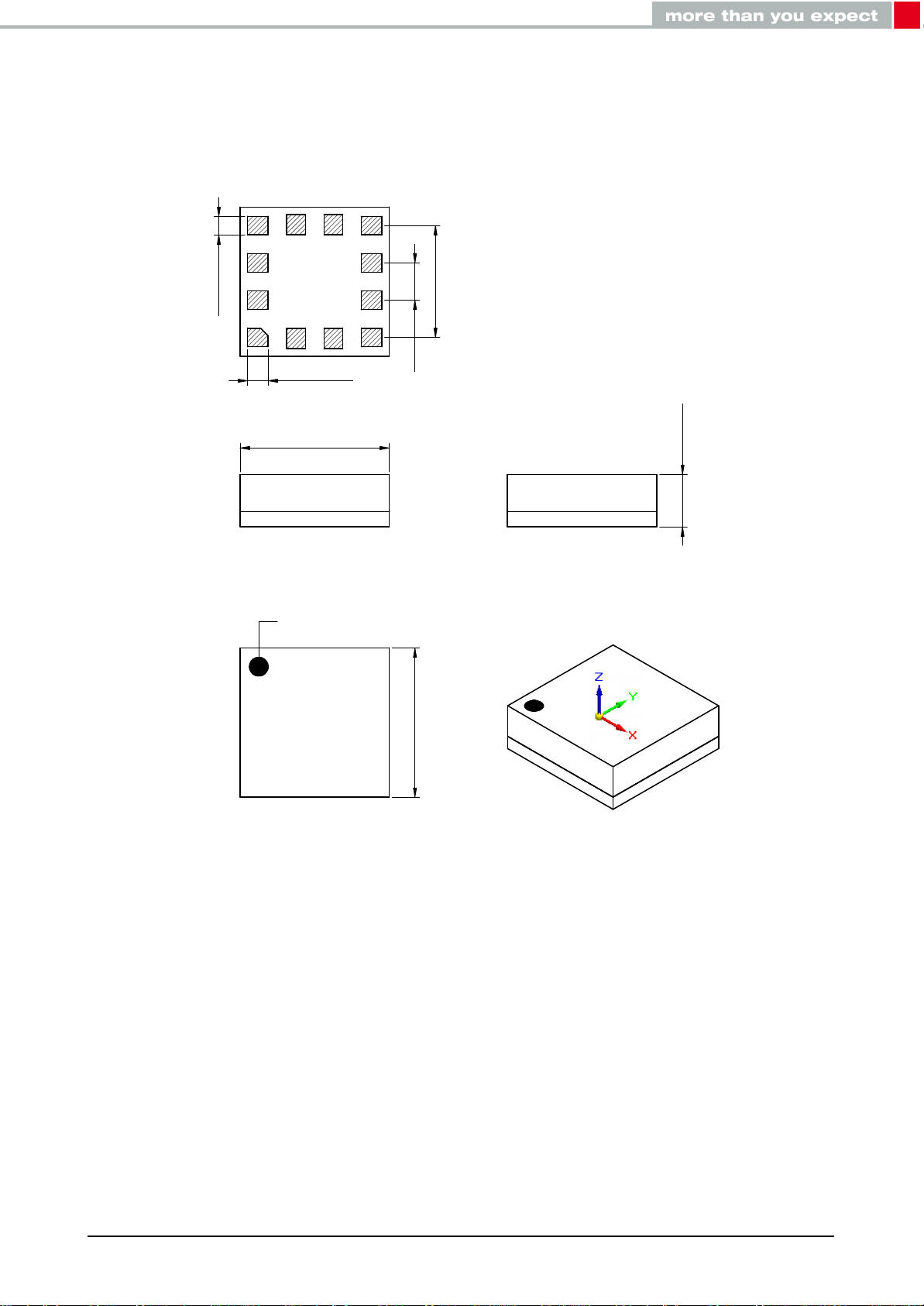
19 Physical dimensions
1
2
7
10
3
4
65
1112
9
8
2,0 ±0,1
0,7 max.
Pin 1
2,0 ±0,1
0,5 ±0,04
1,5 ±0,04
0,25 ±0,04
0,275 ±0,04
19.1 Module drawing
Figure 31: Sensor dimensions [mm]
Acceleration sensor, Part Nr. 2533020201601
User manual version 2.0 © December 2020
www.we-online.com/sensors 83
Page 85
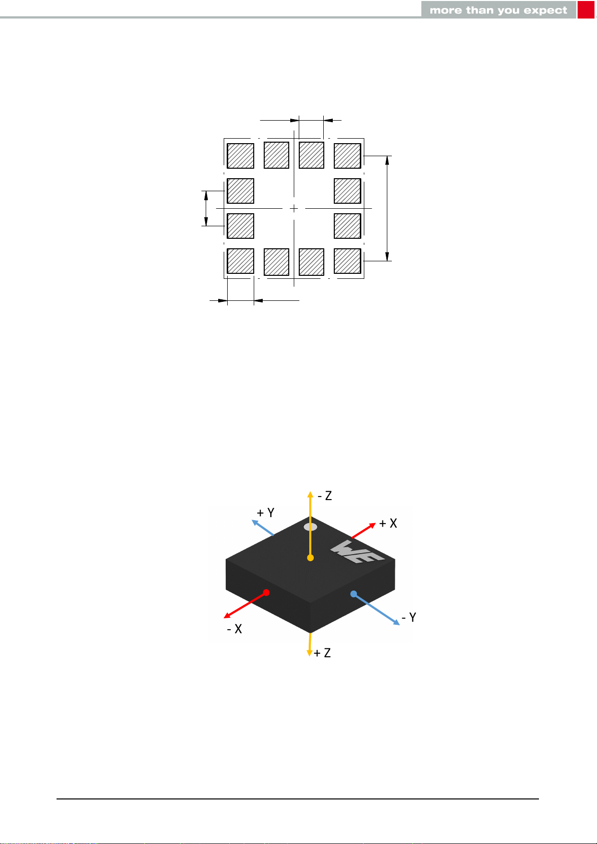
19.2 Footprint
1
4
2
3
5 6
7
8
9
10
1112
1,5
0,375
0,5
0,35
- Y
- Z
- X
+ Z
+ X
+ Y
Figure 32: Recommended land pattern [mm] (top view)
19.3 Measurement axis of the sensor
Figure 33: Measurement axis of the sensor
Acceleration sensor, Part Nr. 2533020201601
User manual version 2.0 © December 2020
www.we-online.com/sensors 84
Page 86

20 Manufacturing information
20.1 Moisture sensitivity level
The sensor product is categorized as JEDEC Moisture Sensitivity Level 3 (MSL3), which requires special handling.
More information regarding the MSL requirements can be found in the IPC/JEDEC J-STD-020
standard on www.jedec.org. More information about the handling, picking, shipping and the
usage of moisture/re-flow and/or process sensitive products can be found in the IPC/JEDEC
J-STD-033 standard on www.jedec.org.
20.2 Soldering
20.2.1 Reflow soldering
Attention must be paid on the thickness of the solder resist between the host PCB top
side and the modules bottom side. Only lead-free assembly is recommended according
to JEDEC J-STD020.
Profile feature Value
Preheat temperature Min T
Preheat temperature Max T
Preheat time from T
S Min
to T
S Max
S Min
S Max
t
S
150°C
200°C
60 - 120 seconds
Ramp-up rate (TLto TP) 3°C / second max.
Liquidous temperature T
Time tLmaintained above T
L
Peak package body temperature T
Time within 5°C of actual preak temperature t
L
t
L
P
P
217°C
60 - 150 seconds
see table below
20 - 30 seconds
Ramp-down Rate (TPto TL)* 6°C / second max.
Time 20°C to T
P
8 minutes max.
Table 100: Classification reflow soldering profile, Note: refer to IPC/JEDEC J-STD-020E
* In order to reduce residual stress on the sensor component, the recommended
ramp-down temperature slope should be lower than 3°C /s.
Acceleration sensor, Part Nr. 2533020201601
User manual version 2.0 © December 2020
www.we-online.com/sensors 85
Page 87
Package thickness
Time
Temperature
T
p
t
p
t
L
t
S
T
s max
T
s min
TC –5°C
T
L
25
Time 25°C to Peak
Preheat Area
Max. Ramp Up Rate
Max. Ramp Down Rate
Volume mm
<350
3
Volume mm
350-2000
3
Volume mm
3
>2000
< 1.6mm 260°C 260°C 260°C
1.6mm - 2.5mm 260°C 250°C 245°C
> 2.5mm 250°C 245°C 245°C
Table 101: Package classification reflow temperature, PB-free assembly, Note: refer to IPC/-
JEDEC J-STD-020E
It is recommended to solder the sensor on the last re-flow cycle of the PCB. For solder paste
use a LFM-48W or Indium based SAC 305 alloy (Sn 96.5 / Ag 3.0 / Cu 0.5 / Indium 8.9HF /
Type 3 / 89%) type 3 or higher.
The reflow profile must be adjusted based on the thermal mass of the entire populated PCB,
heat transfer efficiency of the re-flow oven and the specific type of solder paste used. Based
on the specific process and PCB layout the optimal soldering profile must be adjusted and
verified. Other soldering methods (e.g. vapor phase) have not been verified and have to be
validated by the customer at their own risk. Rework is not recommended.
Figure 34: Reflow soldering profile
After reflow soldering, visually inspect the board to confirm proper alignment
Acceleration sensor, Part Nr. 2533020201601
User manual version 2.0 © December 2020
www.we-online.com/sensors 86
Page 88

20.2.2 Cleaning and washing
Do not clean the product. Any residue cannot be easily removed by washing. Use a "no
clean" soldering paste and do not clean the board after soldering.
• Washing agents used during the production to clean the customer application might
damage or change the characteristics of the component. Washing agents may have a
negative effect on the long-term functionality of the product.
• Using a brush during the cleaning process may damage the component. Therefore,
we do not recommend using a brush during the PCB cleaning process
20.2.3 Potting and coating
• Potting material might shrink or expand during and after hardening. This might apply mechanical stress on the components, which can influence the characteristics of
the transfer function. In addition, potting material can close existing openings in the
housing. This can lead to a malfunction of the component. Thus, potting is not recommended.
• Conformal coating may affect the product performance. We do not recommend coating
the components.
20.2.4 Storage conditions
• A storage of Würth Elektronik eiSos products for longer than 12 months is not recommended. Within other effects, the terminals may suffer degradation, resulting in
bad solderability. Therefore, all products shall be used within the period of 12 months
based on the day of shipment.
• Do not expose the components to direct sunlight.
• The storage conditions in the original packaging are defined according to
DIN EN 61760 - 2.
• For a moisture sensitive component, the storage condition in the original packaging
is defined according to IPC/JEDEC-J-STD-033. It is also recommended to return the
component to the original moisture proof bag and reseal the moisture proof bag again.
20.2.5 Handling
• Violation of the technical product specifications such as exceeding the nominal rated
supply voltage, will void the warranty.
• Violation of the technical product specifications such as but not limited to exceeding
the absolute maximum ratings will void the conformance to regulatory requirements.
• ESD prevention methods need to be followed for manual handling and processing by
machinery.
• The edge castellation is designed and made for prototyping, i.e. hand soldering purposes only.
Acceleration sensor, Part Nr. 2533020201601
User manual version 2.0 © December 2020
www.we-online.com/sensors 87
Page 89

• The applicable country regulations and specific environmental regulations must be observed.
• Do not disassemble the product. Evidence of tampering will void the warranty.
Acceleration sensor, Part Nr. 2533020201601
User manual version 2.0 © December 2020
www.we-online.com/sensors 88
Page 90

21 Important notes
The following conditions apply to all goods within the sensors product range of Würth Elektronik eiSos GmbH & Co. KG:
21.1 General customer responsibility
Some goods within the product range of Würth Elektronik eiSos GmbH & Co. KG contain
statements regarding general suitability for certain application areas. These statements
about suitability are based on our knowledge and experience of typical requirements concerning the areas, serve as general guidance and cannot be estimated as binding statements
about the suitability for a customer application. The responsibility for the applicability and use
in a particular customer design is always solely within the authority of the customer. Due to
this fact, it is up to the customer to evaluate, where appropriate to investigate and to decide
whether the device with the specific product characteristics described in the product specification is valid and suitable for the respective customer application or not. Accordingly, the
customer is cautioned to verify that the documentation is current before placing orders.
21.2 Customer responsibility related to specific, in particular
safety-relevant applications
It has to be clearly pointed out that the possibility of a malfunction of electronic components
or failure before the end of the usual lifetime cannot be completely eliminated in the current
state of the art, even if the products are operated within the range of the specifications.
The same statement is valid for all software and software parts contained in or used with
or for products in the sensor product range of Würth Elektronik eiSos GmbH & Co. KG.
In certain customer applications requiring a high level of safety and especially in customer
applications in which the malfunction or failure of an electronic component could endanger
human life or health, it must be ensured by most advanced technological aid of suitable
design of the customer application that no injury or damage is caused to third parties in the
event of malfunction or failure of an electronic component.
21.3 Best care and attention
Any product-specific data sheets, manuals, application notes, PCN’s, warnings and cautions must be strictly observed in the most recent versions and matching to the products
revisions. This documents can be downloaded from the product specific sections on the
wireless connectivity and sensors homepage.
21.4 Customer support for product specifications
Some products within the product range may contain substances, which are subject to restrictions in certain jurisdictions in order to serve specific technical requirements. Necessary
information is available on request. In this case, the field sales engineer or the internal sales
person in charge should be contacted who will be happy to support in this matter.
Acceleration sensor, Part Nr. 2533020201601
User manual version 2.0 © December 2020
www.we-online.com/sensors 89
Page 91

21.5 Product improvements
Due to constant product improvement, product specifications may change from time to time.
As a standard reporting procedure of the Product Change Notification (PCN) according to
the JEDEC-Standard, we inform about major changes. In case of further queries regarding
the PCN, the field sales engineer, the internal sales person or the technical support team in
charge should be contacted. The basic responsibility of the customer as per section
and
21.2
remains unaffected.
The sensor driver software ¨Sensor SDK¨ and it’s source codes are not subject to the Product Change Notification information process.
21.1
21.6 Product life cycle
Due to technical progress and economical evaluation we also reserve the right to discontinue production and delivery of products. As a standard reporting procedure of the Product
Termination Notification (PTN) according to the JEDEC-Standard we will inform at an early
stage about inevitable product discontinuance. According to this, we cannot ensure that all
products within our product range will always be available. Therefore, it needs to be verified
with the field sales engineer or the internal sales person in charge about the current product
availability expectancy before or when the product for application design-in disposal is considered. The approach named above does not apply in the case of individual agreements
deviating from the foregoing for customer-specific products.
21.7 Property rights
All the rights for contractual products produced by Würth Elektronik eiSos GmbH & Co. KG
on the basis of ideas, development contracts as well as models or templates that are subject
to copyright, patent or commercial protection supplied to the customer will remain with Würth
Elektronik eiSos GmbH & Co. KG. Würth Elektronik eiSos GmbH & Co. KG does not warrant
or represent that any license, either expressed or implied, is granted under any patent right,
copyright, mask work right, or other intellectual property right relating to any combination,
application, or process in which Würth Elektronik eiSos GmbH & Co. KG components or
services are used.
21.8 General terms and conditions
Unless otherwise agreed in individual contracts, all orders are subject to the current version of the "General Terms and Conditions of Würth Elektronik eiSos Group", last version
available at www.we-online.com.
Acceleration sensor, Part Nr. 2533020201601
User manual version 2.0 © December 2020
www.we-online.com/sensors 90
Page 92

22 Legal notice
22.1 Exclusion of liability
Würth Elektronik eiSos GmbH & Co. KG considers the information in this document to be
correct at the time of publication. However, Würth Elektronik eiSos GmbH & Co. KG reserves the right to modify the information such as technical specifications or functions of
its products or discontinue the production of these products or the support of one of these
products without any written announcement or notification to customers. The customer must
make sure that the information used corresponds to the latest published information. Würth
Elektronik eiSos GmbH & Co. KG does not assume any liability for the use of its products.
Würth Elektronik eiSos GmbH & Co. KG does not grant licenses for its patent rights or for
any other of its intellectual property rights or third-party rights.
Notwithstanding anything above, Würth Elektronik eiSos GmbH & Co. KG makes no representations and/or warranties of any kind for the provided information related to their accuracy,
correctness, completeness, usage of the products and/or usability for customer applications.
Information published by Würth Elektronik eiSos GmbH & Co. KG regarding third-party products or services does not constitute a license to use such products or services or a warranty
or endorsement thereof.
22.2 Suitability in customer applications
The customer bears the responsibility for compliance of systems or units, in which Würth
Elektronik eiSos GmbH & Co. KG products are integrated, with applicable legal regulations.
Customer acknowledges and agrees that it is solely responsible for compliance with all legal, regulatory and safety-related requirements concerning its products, and any use of
Würth Elektronik eiSos GmbH & Co. KG components in its applications, notwithstanding
any applications-related in-formation or support that may be provided by Würth Elektronik eiSos GmbH & Co. KG. Customer represents and agrees that it has all the necessary
expertise to create and implement safeguards which anticipate dangerous consequences of
failures, monitor failures and their consequences lessen the likelihood of failures that might
cause harm and take appropriate remedial actions. The customer will fully indemnify Würth
Elektronik eiSos GmbH & Co. KG and its representatives against any damages arising out
of the use of any Würth Elektronik eiSos GmbH & Co. KG components in safety-critical
applications.
22.3 Usage restriction
Würth Elektronik eiSos GmbH & Co. KG products have been designed and developed for
usage in general electronic equipment only. This product is not authorized for use in equipment where a higher safety standard and reliability standard is especially required or where
a failure of the product is reasonably expected to cause severe personal injury or death,
unless the parties have executed an agreement specifically governing such use. Moreover,
Würth Elektronik eiSos GmbH & Co. KG products are neither designed nor intended for use
in areas such as military, aerospace, aviation, nuclear control, submarine, transportation
(automotive control, train control, ship control), transportation signal, disaster prevention,
medical, public information network etc. Würth Elektronik eiSos GmbH & Co. KG must be
Acceleration sensor, Part Nr. 2533020201601
User manual version 2.0 © December 2020
www.we-online.com/sensors 91
Page 93

informed about the intent of such usage before the design-in stage. In addition, sufficient
reliability evaluation checks for safety must be performed on every electronic component,
which is used in electrical circuits that require high safety and reliability function or performance. By using Würth Elektronik eiSos GmbH & Co. KG products, the customer agrees to
these terms and conditions.
Acceleration sensor, Part Nr. 2533020201601
User manual version 2.0 © December 2020
www.we-online.com/sensors 92
Page 94

23 License terms for Würth Elektronik eiSos
GmbH & Co. KG sensor product software and source
code
This License terms will take effect upon the purchase and usage of the Würth Elektronik
eiSos GmbH & Co. KG sensor products. You hereby agree that this license terms are applicable to the product and the incorporated software, firmware and source codes (collectively,
"Software") made available by Würth Elektronik eiSos in any form, including but not limited
to binary, executable or source code form.
The software included in any Würth Elektronik eiSos sensor product is purchased to you on
the condition that you accept the terms and conditions of this license terms. You agree to
comply with all provisions under this license terms.
23.1 Limited license
Würth Elektronik eiSos hereby grants you a limited, non-exclusive, non-transferable and
royalty-free license to use the software and under the conditions that will be set forth in this
license terms. You are free to use the provided software only in connection with one of the
products from Würth Elektronik eiSos to the extent described in this license terms.
You are entitled to change or alter the source code for the sole purpose of creating an application embedding the Würth Elektronik eiSos sensor product. The transfer of the source
code to third parties is allowed to the sole extent that the source code is used by such third
parties in connection with our product or another hardware provided by Würth Elektronik
eiSos under strict adherence of this license terms. Würth Elektronik eiSos will not assume
any liability for the usage of the incorporated software and the source code.
You are not entitled to transfer the source code in any form to third parties without prior written consent of Würth Elektronik eiSos.
You are not allowed to reproduce, translate, reverse engineer, decompile, disassemble or
create derivative works of the incorporated software and the source code in whole or in part.
No more extensive rights to use and exploit the products are granted to you.
23.2 Usage and obligations
The responsibility for the applicability and use of the Würth Elektronik eiSos sensor product
with the incorporated software in a particular customer design is always solely within the
authority of the customer. Due to this fact, it is up to you to evaluate and investigate, where
appropriate, and to decide whether the device with the specific product characteristics described in the product specification is valid and suitable for your respective application or
not.
You are responsible for using the Würth Elektronik eiSos sensor product with the incorporated software in compliance with all applicable product liability and product safety laws. You
acknowledge to minimize the risk of loss and harm to individuals and bear the risk for failure
leading to personal injury or death due to your usage of the product.
Würth Elektronik eiSos’ products are not authorized for use in safety-critical applications,
or where a failure of the product is reasonably expected to cause severe personal injury
or death. Moreover, Würth Elektronik eiSos’ products are neither designed nor intended for
Acceleration sensor, Part Nr. 2533020201601
User manual version 2.0 © December 2020
www.we-online.com/sensors 93
Page 95

use in areas such as military, aerospace, aviation, nuclear control, submarine, transportation
(automotive control, train control, ship control), transportation signal, disaster prevention,
medical, public information network etc. You shall inform Würth Elektronik eiSos about the
intent of such usage before design-in stage. In certain customer applications requiring a very
high level of safety and in which the malfunction or failure of an electronic component could
endanger human life or health, you must ensure to have all necessary expertise in the safety
and regulatory ramifications of your applications. You acknowledge and agree that you are
solely responsible for all legal, regulatory and safety-related requirements concerning your
products and any use of Würth Elektronik eiSos’ products in such safety-critical applications, notwithstanding any applications-related information or support that may be provided by
Würth Elektronik eiSos. YOU SHALL INDEMNIFY WÜRTH ELEKTRONIK EISOS AGAINST
ANY DAMAGES ARISING OUT OF THE USE OF WÜRTH ELEKTRONIK EISOS’ PRODUCTS IN SUCH SAFETY-CRITICAL APPLICATIONS.
23.3 Ownership
The incorporated Software created by Würth Elektronik eiSos is and will remain the exclusive
property of Würth Elektronik eiSos.
23.4 Disclaimer of warranty
THE SOFTWARE AND IT’S SOURCE CODE IS PROVIDED "AS IS". YOU ACKNOWLEDGE THAT WÜRTH ELEKTRONIK EISOS MAKES NO REPRESENTATIONS AND WARRANTIES OF ANY KIND RELATED TO, BUT NOT LIMITED TO THE NON-INFRINGEMENT
OF THIRD PARTIES’ INTELLECTUAL PROPERTY RIGHTS OR THE MERCHANTABILITY OR FITNESS FOR YOUR INTENDED PURPOSE OR USAGE. WÜRTH ELEKTRONIK
EISOS DOES NOT WARRANT OR REPRESENT THAT ANY LICENSE, EITHER EXPRESS
OR IMPLIED, IS GRANTED UNDER ANY PATENT RIGHT, COPYRIGHT, MASK WORK
RIGHT, OR OTHER INTELLECTUAL PROPERTY RIGHT RELATING TO ANY COMBINATION, MACHINE, OR PROCESS IN WHICH THE WÜRTH ELEKTRONIK EISOS’ PRODUCT WITH THE INCORPORATED SOFTWARE IS USED. INFORMATION PUBLISHED BY
WÜRTH ELEKTRONIK EISOS REGARDING THIRD-PARTY PRODUCTS OR SERVICES
DOES NOT CONSTITUTE A LICENSE FROM WÜRTH ELEKTRONIK EISOS TO USE
SUCH PRODUCTS OR SERVICES OR A WARRANTY OR ENDORSEMENT THEREOF.
23.5 Limitation of liability
Any liability not expressly provided by Würth Elektronik eiSos shall be disclaimed.
You agree to hold us harmless from any third-party claims related to your usage of the Würth
Elektronik eiSos’ products with the incorporated software and source code. Würth Elektronik
eiSos disclaims any liability for any alteration, development created by you or your customers
as well as for any combination with other products.
23.6 Applicable law and jurisdiction
Applicable law to this license terms shall be the laws of the Federal Republic of Germany.
Any dispute, claim or controversy arising out of or relating to this license terms shall be
Acceleration sensor, Part Nr. 2533020201601
User manual version 2.0 © December 2020
www.we-online.com/sensors 94
Page 96

resolved and finally settled by the court competent for the location of Würth Elektronik eiSos
registered office.
23.7 Severability clause
If a provision of this license terms are or becomes invalid, unenforceable or null and void,
this shall not affect the remaining provisions of the terms. The parties shall replace any such
provisions with new valid provisions that most closely approximate the purpose of the terms.
23.8 Miscellaneous
Würth Elektronik eiSos reserves the right at any time to change this terms at its own discretion. It is your responsibility to check at Würth Elektronik eiSos homepage for any updates.
Your continued usage of the products will be deemed as the acceptance of the change.
We recommend you to be updated about the status of new software, which is available on
our website or in our data sheet, and to implement new software in your device where appropriate.
By ordering a sensor product, you accept this license terms in all terms.
Acceleration sensor, Part Nr. 2533020201601
User manual version 2.0 © December 2020
www.we-online.com/sensors 95
Page 97

List of Figures
1 Block diagram . . . . . . . . . . . . . . . . . . . . . . . . . . . . . . . . . . . . 8
2 Pinout (top view) . . . . . . . . . . . . . . . . . . . . . . . . . . . . . . . . . . 13
3 Electrical connection (top view) . . . . . . . . . . . . . . . . . . . . . . . . . . 14
4 Master-slave concept . . . . . . . . . . . . . . . . . . . . . . . . . . . . . . . 15
5 SDA and SCL logic levels . . . . . . . . . . . . . . . . . . . . . . . . . . . . . 16
6 Data validity, START and STOP condition . . . . . . . . . . . . . . . . . . . . 17
7 Slave address format . . . . . . . . . . . . . . . . . . . . . . . . . . . . . . . . 18
8 Complete data transfer . . . . . . . . . . . . . . . . . . . . . . . . . . . . . . . 18
9 Write and read operations of the sensor . . . . . . . . . . . . . . . . . . . . . 19
10 SPI Interface . . . . . . . . . . . . . . . . . . . . . . . . . . . . . . . . . . . . 21
11 SPI register address . . . . . . . . . . . . . . . . . . . . . . . . . . . . . . . . 23
12 4-wire SPI data transfer (CPOL = 1, CPHA = 1) . . . . . . . . . . . . . . . . . 23
13 SPI write protocol . . . . . . . . . . . . . . . . . . . . . . . . . . . . . . . . . . 24
14 SPI read protocol . . . . . . . . . . . . . . . . . . . . . . . . . . . . . . . . . . 24
15 Communication check . . . . . . . . . . . . . . . . . . . . . . . . . . . . . . . 28
16 Sensor in operation with high performance mode . . . . . . . . . . . . . . . . 29
17 Sensor in operation with single data conversion mode . . . . . . . . . . . . . 31
18 Single data conversion using an external trigger signal . . . . . . . . . . . . . 34
19 Block diagram of filtering chain . . . . . . . . . . . . . . . . . . . . . . . . . . 37
20 High pass filter without REFERENCE mode . . . . . . . . . . . . . . . . . . . 40
21 High pass filter with REFERENCE mode . . . . . . . . . . . . . . . . . . . . . 40
22 First-in First-out Buffer . . . . . . . . . . . . . . . . . . . . . . . . . . . . . . . 41
23 Bypass mode . . . . . . . . . . . . . . . . . . . . . . . . . . . . . . . . . . . . 42
24 FIFO mode . . . . . . . . . . . . . . . . . . . . . . . . . . . . . . . . . . . . . 43
25 FIFO mode interrupts . . . . . . . . . . . . . . . . . . . . . . . . . . . . . . . 44
26 Continuous mode . . . . . . . . . . . . . . . . . . . . . . . . . . . . . . . . . . 45
27 Continuous to FIFO mode . . . . . . . . . . . . . . . . . . . . . . . . . . . . . 46
28 Bypass to Continuous mode . . . . . . . . . . . . . . . . . . . . . . . . . . . . 47
29 DRDY signal . . . . . . . . . . . . . . . . . . . . . . . . . . . . . . . . . . . . 51
30 Self test procedure . . . . . . . . . . . . . . . . . . . . . . . . . . . . . . . . . 54
31 Sensor dimensions [mm] . . . . . . . . . . . . . . . . . . . . . . . . . . . . . 83
32 Recommended land pattern [mm] (top view) . . . . . . . . . . . . . . . . . . . 84
33 Measurement axis of the sensor . . . . . . . . . . . . . . . . . . . . . . . . . 84
34 Reflow soldering profile . . . . . . . . . . . . . . . . . . . . . . . . . . . . . . 86
List of Tables
1 Ordering information . . . . . . . . . . . . . . . . . . . . . . . . . . . . . . . . 8
2 Acceleration sensor specification . . . . . . . . . . . . . . . . . . . . . . . . . 9
3 Acceleration sensitivity parameter . . . . . . . . . . . . . . . . . . . . . . . . 10
4 Temperature sensor specification . . . . . . . . . . . . . . . . . . . . . . . . . 10
5 Electrical specification . . . . . . . . . . . . . . . . . . . . . . . . . . . . . . . 11
6 Absolute maximum rating . . . . . . . . . . . . . . . . . . . . . . . . . . . . . 12
7 General information . . . . . . . . . . . . . . . . . . . . . . . . . . . . . . . . 12
8 Pin description . . . . . . . . . . . . . . . . . . . . . . . . . . . . . . . . . . . 13
9 Internal pull up values (typ) for SAO and CS pins . . . . . . . . . . . . . . . . 14
Acceleration sensor, Part Nr. 2533020201601
User manual version 2.0 © December 2020
www.we-online.com/sensors 96
Page 98

10 Slave address and Read/Write commands . . . . . . . . . . . . . . . . . . . . 19
11 I2C timing parameters . . . . . . . . . . . . . . . . . . . . . . . . . . . . . . . 20
12 SPI communication modes . . . . . . . . . . . . . . . . . . . . . . . . . . . . 22
13 SPI timing parameters . . . . . . . . . . . . . . . . . . . . . . . . . . . . . . . 25
14 Time consumption . . . . . . . . . . . . . . . . . . . . . . . . . . . . . . . . . 28
15 Acceleration resolution . . . . . . . . . . . . . . . . . . . . . . . . . . . . . . . 32
16 Current consumption (µA) . . . . . . . . . . . . . . . . . . . . . . . . . . . . . 33
17 Noise density at ODR = 200 Hz (µg /√Hz) . . . . . . . . . . . . . . . . . . . . 33
18 Conversion time . . . . . . . . . . . . . . . . . . . . . . . . . . . . . . . . . . 34
19 Output data rate . . . . . . . . . . . . . . . . . . . . . . . . . . . . . . . . . . 35
20 Low pass filter 1 . . . . . . . . . . . . . . . . . . . . . . . . . . . . . . . . . . 38
21 Low pass filter_1 + Low pass filter _2 . . . . . . . . . . . . . . . . . . . . . . . 38
22 Low pass filter_1 + High pass filter . . . . . . . . . . . . . . . . . . . . . . . . 39
23 FIFO_Samples register . . . . . . . . . . . . . . . . . . . . . . . . . . . . . . 47
24 Threshold function . . . . . . . . . . . . . . . . . . . . . . . . . . . . . . . . . 49
25 CTRL_4 . . . . . . . . . . . . . . . . . . . . . . . . . . . . . . . . . . . . . . . 50
26 CTRL_5 . . . . . . . . . . . . . . . . . . . . . . . . . . . . . . . . . . . . . . . 50
27 Temperature refresh rate . . . . . . . . . . . . . . . . . . . . . . . . . . . . . . 57
28 Temperature look up table . . . . . . . . . . . . . . . . . . . . . . . . . . . . . 58
29 T_OUT_L register . . . . . . . . . . . . . . . . . . . . . . . . . . . . . . . . . 60
30 T_OUT_L register description . . . . . . . . . . . . . . . . . . . . . . . . . . . 60
31 T_OUT_H register . . . . . . . . . . . . . . . . . . . . . . . . . . . . . . . . . 60
32 T_OUT_H register description . . . . . . . . . . . . . . . . . . . . . . . . . . . 61
33 Device_ID register . . . . . . . . . . . . . . . . . . . . . . . . . . . . . . . . . 61
34 CTRL_1 register . . . . . . . . . . . . . . . . . . . . . . . . . . . . . . . . . . 61
35 Output data rate configuration . . . . . . . . . . . . . . . . . . . . . . . . . . . 61
36 Mode selection . . . . . . . . . . . . . . . . . . . . . . . . . . . . . . . . . . . 62
37 Normal and Low power mode selection . . . . . . . . . . . . . . . . . . . . . 62
38 CTRL_2 register . . . . . . . . . . . . . . . . . . . . . . . . . . . . . . . . . . 62
39 CTRL_2 register description . . . . . . . . . . . . . . . . . . . . . . . . . . . . 62
40 CTRL_3 register . . . . . . . . . . . . . . . . . . . . . . . . . . . . . . . . . . 63
41 CTRL_3 register description . . . . . . . . . . . . . . . . . . . . . . . . . . . . 63
42 Self-test mode . . . . . . . . . . . . . . . . . . . . . . . . . . . . . . . . . . . 64
43 CTRL_4 register . . . . . . . . . . . . . . . . . . . . . . . . . . . . . . . . . . 64
44 CTRL_4 register description . . . . . . . . . . . . . . . . . . . . . . . . . . . . 64
45 CTRL_5 register . . . . . . . . . . . . . . . . . . . . . . . . . . . . . . . . . . 65
46 CTRL_5 register description . . . . . . . . . . . . . . . . . . . . . . . . . . . . 65
47 CTRL_6 register . . . . . . . . . . . . . . . . . . . . . . . . . . . . . . . . . . 66
48 CTRL_6 register description . . . . . . . . . . . . . . . . . . . . . . . . . . . . 66
49 Filtering cut-off selection . . . . . . . . . . . . . . . . . . . . . . . . . . . . . . 66
50 Full scale selection . . . . . . . . . . . . . . . . . . . . . . . . . . . . . . . . . 66
51 T_OUT register . . . . . . . . . . . . . . . . . . . . . . . . . . . . . . . . . . . 66
52 T_OUT register description . . . . . . . . . . . . . . . . . . . . . . . . . . . . 67
53 STATUS register . . . . . . . . . . . . . . . . . . . . . . . . . . . . . . . . . . 67
54 STATUS register . . . . . . . . . . . . . . . . . . . . . . . . . . . . . . . . . . 67
55 X_OUT_L register . . . . . . . . . . . . . . . . . . . . . . . . . . . . . . . . . 68
56 X_OUT_L registerr description . . . . . . . . . . . . . . . . . . . . . . . . . . 68
57 X_OUT_H register . . . . . . . . . . . . . . . . . . . . . . . . . . . . . . . . . 68
58 Y_OUT_L register . . . . . . . . . . . . . . . . . . . . . . . . . . . . . . . . . 69
Acceleration sensor, Part Nr. 2533020201601
User manual version 2.0 © December 2020
www.we-online.com/sensors 97
Page 99

59 Y_OUT_L register description . . . . . . . . . . . . . . . . . . . . . . . . . . . 69
60 Y_OUT_H register . . . . . . . . . . . . . . . . . . . . . . . . . . . . . . . . . 69
61 Z_OUT_L register . . . . . . . . . . . . . . . . . . . . . . . . . . . . . . . . . 70
62 Z_OUT_L register description . . . . . . . . . . . . . . . . . . . . . . . . . . . 70
63 Z_OUT_H register . . . . . . . . . . . . . . . . . . . . . . . . . . . . . . . . . 70
64 FIFO_CTRL register . . . . . . . . . . . . . . . . . . . . . . . . . . . . . . . . 70
65 FIFO_CTRL register description . . . . . . . . . . . . . . . . . . . . . . . . . 71
66 FIFO_SAMPLES register . . . . . . . . . . . . . . . . . . . . . . . . . . . . . 71
67 FIFO_SAMPLES register description . . . . . . . . . . . . . . . . . . . . . . . 71
68 TAP_X_TH register . . . . . . . . . . . . . . . . . . . . . . . . . . . . . . . . . 71
69 TAP_X_TH register description . . . . . . . . . . . . . . . . . . . . . . . . . . 72
70 4D/6D threshold setting FS: ±2g description . . . . . . . . . . . . . . . . . . . 72
71 TAP_Y_TH register . . . . . . . . . . . . . . . . . . . . . . . . . . . . . . . . . 72
72 TAP_Y_TH register description . . . . . . . . . . . . . . . . . . . . . . . . . . 72
73 Axis priority for tap detection . . . . . . . . . . . . . . . . . . . . . . . . . . . 72
74 TAP_Z_TH register . . . . . . . . . . . . . . . . . . . . . . . . . . . . . . . . . 73
75 TAP_Z_TH register description . . . . . . . . . . . . . . . . . . . . . . . . . . 73
76 INT_DUR register . . . . . . . . . . . . . . . . . . . . . . . . . . . . . . . . . 73
77 INT_DUR register description . . . . . . . . . . . . . . . . . . . . . . . . . . . 73
78 WAKE_UP_TH register . . . . . . . . . . . . . . . . . . . . . . . . . . . . . . 74
79 WAKE_UP_TH register description . . . . . . . . . . . . . . . . . . . . . . . . 74
80 WAKE_UP_DUR register . . . . . . . . . . . . . . . . . . . . . . . . . . . . . 74
81 WAKE_UP_DUR register description . . . . . . . . . . . . . . . . . . . . . . . 74
82 FREE_FALL register . . . . . . . . . . . . . . . . . . . . . . . . . . . . . . . . 75
83 FREE_FALL register description . . . . . . . . . . . . . . . . . . . . . . . . . 75
84 FREE_FALL threshold . . . . . . . . . . . . . . . . . . . . . . . . . . . . . . . 75
85 STATUS_DETECT register . . . . . . . . . . . . . . . . . . . . . . . . . . . . 76
86 STATUS_DETECT register description . . . . . . . . . . . . . . . . . . . . . . 76
87 WAKE_UP_EVENT register . . . . . . . . . . . . . . . . . . . . . . . . . . . . 77
88 WAKE_UP_EVENT register description . . . . . . . . . . . . . . . . . . . . . 77
89 TAP_EVENT register . . . . . . . . . . . . . . . . . . . . . . . . . . . . . . . . 78
90 TAP_EVENT register description . . . . . . . . . . . . . . . . . . . . . . . . . 78
91 6D_EVENT register . . . . . . . . . . . . . . . . . . . . . . . . . . . . . . . . 79
92 6D_EVENT register description . . . . . . . . . . . . . . . . . . . . . . . . . . 79
93 ALL_INT_EVENT register . . . . . . . . . . . . . . . . . . . . . . . . . . . . . 80
94 ALL_INT_EVENT register description . . . . . . . . . . . . . . . . . . . . . . 80
95 X_OFS_USR register . . . . . . . . . . . . . . . . . . . . . . . . . . . . . . . 81
96 Y_OFS_USR register . . . . . . . . . . . . . . . . . . . . . . . . . . . . . . . 81
97 Z_OFS_USR register . . . . . . . . . . . . . . . . . . . . . . . . . . . . . . . 81
98 CTRL_7 register . . . . . . . . . . . . . . . . . . . . . . . . . . . . . . . . . . 82
99 CTRL_7 register description . . . . . . . . . . . . . . . . . . . . . . . . . . . . 82
100 Classification reflow soldering profile, Note: refer to IPC/JEDEC J-STD-020E 85
101 Package classification reflow temperature, PB-free assembly, Note: refer to
IPC/JEDEC J-STD-020E . . . . . . . . . . . . . . . . . . . . . . . . . . . . . 86
Acceleration sensor, Part Nr. 2533020201601
User manual version 2.0 © December 2020
www.we-online.com/sensors 98
Page 100
Monitoring
& Control
Automated Meter
Reading
Internet
of Things
more than you expect
Contact:
Würth Elektronik eiSos GmbH & Co. KG
Division Wireless Connectivity & Sensors
Max-Eyth-Straße 1
74638 Waldenburg
Germany
Tel.: +49 651 99355-0
Fax.: +49 651 99355-69
www.we-online.com/wireless-connectivity
 Loading...