

Page 1

ABSOLUTE PRESSURE SENSOR
WSEN-PADS
USER MANUAL
2511020213301
VERSION 2.0
NOVEMBER 11, 2020
Page 2
Revision history
Manual
version
0.1
1.0
1.1
Notes Date
• Initial release of the manual
• Updated section11: Interrupt functionality
• Updated section13: Register description
• Updated flowchart in section
• Added note to section
• Updated section
pressure threshold
• Updated address of reserved registers and register type of
REF_P_x in section12: Register Map
• Updated register name in section
9.3
11.2
: Interrupt generation based on
7.5
13.6
April 2019
June 2019
April 2020
2.0
• Updated register address to 0x7C in section
• Added description of the SPI interface.
• Updated pin description for the SPI interface in section
• Added ’SIM’ bit for the SPI interface in section12and
under register description in section
13.6
13.28
3.2
November 2020
Absolute pressure sensor, Part Nr. 2511020213301
User manual version 2.0 © November2020
www.we-online.com/sensors 1
Page 3

Abbreviations
Abbreviation Description
ASIC Application Specific Integrated Circuit
BDU Block Data Update
DRDY Data ready
ESD Electrostatic Discharge
FIFO First-In First-Out
HBM Human Body Model
I2C Inter Integrated Circuit
LGA Land Grid Array
LSB Least Significant Bit
MEMS Micro-Electro Mechanical System
MISO Master In Slabe Out
MOSI Master Out Slave In
MSB Most Significant Bit
NVM Non Volatile Memory
ODR Output Data Rate
PCB Printed Circuit Board
SPI Serial Peripheral Interface
Absolute pressure sensor, Part Nr. 2511020213301
User manual version 2.0 © November2020
www.we-online.com/sensors 2
Page 4

Contents
1 Introduction 7
1.1 Application . . . . . . . . . . . . . . . . . . . . . . . . . . . . . . . . . . . . 7
1.2 Key features . . . . . . . . . . . . . . . . . . . . . . . . . . . . . . . . . . . . 7
1.3 Ordering information . . . . . . . . . . . . . . . . . . . . . . . . . . . . . . . 7
1.4 Block diagram . . . . . . . . . . . . . . . . . . . . . . . . . . . . . . . . . . . 8
1.5 Operational functionality . . . . . . . . . . . . . . . . . . . . . . . . . . . . . 8
1.5.1 MEMS Cell . . . . . . . . . . . . . . . . . . . . . . . . . . . . . . . . 8
1.5.2 ASIC . . . . . . . . . . . . . . . . . . . . . . . . . . . . . . . . . . . 8
1.5.3 Calibration . . . . . . . . . . . . . . . . . . . . . . . . . . . . . . . . 8
1.5.4 Digital filtering . . . . . . . . . . . . . . . . . . . . . . . . . . . . . . 9
1.5.5 FIFO memory . . . . . . . . . . . . . . . . . . . . . . . . . . . . . . 9
1.6 Filtering chain and data path . . . . . . . . . . . . . . . . . . . . . . . . . . 9
2 Sensor specifications 10
2.1 General information . . . . . . . . . . . . . . . . . . . . . . . . . . . . . . . 10
2.2 Absolute maximum ratings . . . . . . . . . . . . . . . . . . . . . . . . . . . . 10
2.3 Pressure sensor specification . . . . . . . . . . . . . . . . . . . . . . . . . . 11
2.4 Temperature sensor specification . . . . . . . . . . . . . . . . . . . . . . . . 11
2.5 Electrical specifications . . . . . . . . . . . . . . . . . . . . . . . . . . . . . 12
3 Pinning information 13
3.1 Pin configuration . . . . . . . . . . . . . . . . . . . . . . . . . . . . . . . . . 13
3.2 Pin description . . . . . . . . . . . . . . . . . . . . . . . . . . . . . . . . . . 13
4 Digital I2C interface 14
4.1 General characteristics . . . . . . . . . . . . . . . . . . . . . . . . . . . . . . 14
4.2 SDA and SCL logic levels . . . . . . . . . . . . . . . . . . . . . . . . . . . . 15
4.3 Communication phase . . . . . . . . . . . . . . . . . . . . . . . . . . . . . . 15
4.3.1 Idle state . . . . . . . . . . . . . . . . . . . . . . . . . . . . . . . . . 15
4.3.2 START(S) and STOP(P) condition . . . . . . . . . . . . . . . . . . . 15
4.3.3 Data validity . . . . . . . . . . . . . . . . . . . . . . . . . . . . . . . 16
4.3.4 Byte format . . . . . . . . . . . . . . . . . . . . . . . . . . . . . . . 16
4.3.5 Acknowledge(ACK) and No-Acknowledge(NACK) . . . . . . . . . . 16
4.3.6 Slave address for the sensor . . . . . . . . . . . . . . . . . . . . . . 17
4.3.7 Read/Write operation . . . . . . . . . . . . . . . . . . . . . . . . . . 18
4.4 I2C timing parameters . . . . . . . . . . . . . . . . . . . . . . . . . . . . . . 20
5 Serial Peripheral Interface (SPI) 21
5.1 Data transfer . . . . . . . . . . . . . . . . . . . . . . . . . . . . . . . . . . . 22
5.2 Communcation modes . . . . . . . . . . . . . . . . . . . . . . . . . . . . . . 22
5.3 Sensor SPI Communcation . . . . . . . . . . . . . . . . . . . . . . . . . . . 23
5.3.1 SPI write operation . . . . . . . . . . . . . . . . . . . . . . . . . . . 24
5.3.2 SPI read operation . . . . . . . . . . . . . . . . . . . . . . . . . . . 24
5.3.3 SPI timing parameters . . . . . . . . . . . . . . . . . . . . . . . . . 25
6 Application circuit 26
Absolute pressure sensor, Part Nr. 2511020213301
User manual version 2.0 © November2020
www.we-online.com/sensors 3
Page 5

7 Quick start guide 28
7.1 Power-up sequence . . . . . . . . . . . . . . . . . . . . . . . . . . . . . . . 28
7.2 Communication with host controller . . . . . . . . . . . . . . . . . . . . . . . 29
7.3 Reboot . . . . . . . . . . . . . . . . . . . . . . . . . . . . . . . . . . . . . . . 29
7.4 Software reset . . . . . . . . . . . . . . . . . . . . . . . . . . . . . . . . . . 29
7.5 Sensor operation: single conversion mode . . . . . . . . . . . . . . . . . . . 31
7.6 Sensor operation: continuous mode . . . . . . . . . . . . . . . . . . . . . . 32
7.7 Power-off sequence . . . . . . . . . . . . . . . . . . . . . . . . . . . . . . . 33
8 Modes of operation 34
8.1 Power-down mode . . . . . . . . . . . . . . . . . . . . . . . . . . . . . . . . 35
8.2 Single conversion mode . . . . . . . . . . . . . . . . . . . . . . . . . . . . . 36
8.3 Continuous mode . . . . . . . . . . . . . . . . . . . . . . . . . . . . . . . . . 37
8.4 Additional configurations . . . . . . . . . . . . . . . . . . . . . . . . . . . . . 38
8.4.1 Low-power or low-noise configuration . . . . . . . . . . . . . . . . . 38
8.4.2 Enabling additional low-pass filter . . . . . . . . . . . . . . . . . . . 39
9 Reading output data 40
9.1 Reading pressure values . . . . . . . . . . . . . . . . . . . . . . . . . . . . . 40
9.2 Reading temperature values . . . . . . . . . . . . . . . . . . . . . . . . . . . 41
9.3 Status register for reading the data . . . . . . . . . . . . . . . . . . . . . . . 42
10 FIFO buffer 43
10.1 Bypass mode . . . . . . . . . . . . . . . . . . . . . . . . . . . . . . . . . . . 45
10.2 FIFO mode . . . . . . . . . . . . . . . . . . . . . . . . . . . . . . . . . . . . 46
10.3 Continuous mode . . . . . . . . . . . . . . . . . . . . . . . . . . . . . . . . . 47
10.4 Bypass-to-FIFO mode . . . . . . . . . . . . . . . . . . . . . . . . . . . . . . 48
10.5 Bypass-to-continuous mode . . . . . . . . . . . . . . . . . . . . . . . . . . . 49
10.6 Continuous-to-FIFO mode . . . . . . . . . . . . . . . . . . . . . . . . . . . . 50
10.7 FIFO status monitoring and control . . . . . . . . . . . . . . . . . . . . . . . 51
10.7.1 User-defined FIFO threshold . . . . . . . . . . . . . . . . . . . . . . 52
10.7.2 Reading data from FIFO buffer . . . . . . . . . . . . . . . . . . . . . 52
11 Interrupt functionality 53
11.1 Interrupt generation on pressure data-ready . . . . . . . . . . . . . . . . . . 53
11.2 Interrupt generation based on pressure threshold . . . . . . . . . . . . . . . 54
11.2.1 Interrupt latching . . . . . . . . . . . . . . . . . . . . . . . . . . . . 57
11.3 FIFO status based interrupt events . . . . . . . . . . . . . . . . . . . . . . . 58
11.4 Routing interrupt events to the INT pin . . . . . . . . . . . . . . . . . . . . . 58
12 Register map 60
13 Register description 61
13.1 INT_CFG (0x0B) . . . . . . . . . . . . . . . . . . . . . . . . . . . . . . . . . 61
13.2 THR_P_L (0x0C) . . . . . . . . . . . . . . . . . . . . . . . . . . . . . . . . . 63
13.3 THR_P_H (0x0D) . . . . . . . . . . . . . . . . . . . . . . . . . . . . . . . . . 63
13.4 INTERFACE_CTRL (0x0E) . . . . . . . . . . . . . . . . . . . . . . . . . . . 64
13.5 DEVICE_ID (0x0F) . . . . . . . . . . . . . . . . . . . . . . . . . . . . . . . . 64
13.6 CTRL_1 (0x10) . . . . . . . . . . . . . . . . . . . . . . . . . . . . . . . . . . 65
13.7 CTRL_2 (0x11) . . . . . . . . . . . . . . . . . . . . . . . . . . . . . . . . . . 66
Absolute pressure sensor, Part Nr. 2511020213301
User manual version 2.0 © November2020
www.we-online.com/sensors 4
Page 6

13.8 CTRL_3 (0x12) . . . . . . . . . . . . . . . . . . . . . . . . . . . . . . . . . . 67
13.9 FIFO_CTRL (0x13) . . . . . . . . . . . . . . . . . . . . . . . . . . . . . . . . 68
13.10 FIFO_WTM (0x14) . . . . . . . . . . . . . . . . . . . . . . . . . . . . . . . . 69
13.11 REF_P_L (0x15) . . . . . . . . . . . . . . . . . . . . . . . . . . . . . . . . . 69
13.12 REF_P_H (0x16) . . . . . . . . . . . . . . . . . . . . . . . . . . . . . . . . . 69
13.13 OPC_L (0x18) . . . . . . . . . . . . . . . . . . . . . . . . . . . . . . . . . . . 70
13.14 OPC_H (0x19) . . . . . . . . . . . . . . . . . . . . . . . . . . . . . . . . . . 70
13.15 INT_SOURCE (0x24) . . . . . . . . . . . . . . . . . . . . . . . . . . . . . . 71
13.16 FIFO_STATUS_1 (0x25) . . . . . . . . . . . . . . . . . . . . . . . . . . . . . 71
13.17 FIFO_STATUS_2 (0x26) . . . . . . . . . . . . . . . . . . . . . . . . . . . . . 72
13.18 STATUS (0x27) . . . . . . . . . . . . . . . . . . . . . . . . . . . . . . . . . . 72
13.19 DATA_P_XL (0x28) . . . . . . . . . . . . . . . . . . . . . . . . . . . . . . . . 73
13.20 DATA_P_L (0x29) . . . . . . . . . . . . . . . . . . . . . . . . . . . . . . . . . 73
13.21 DATA_P_H (0x2A) . . . . . . . . . . . . . . . . . . . . . . . . . . . . . . . . 74
13.22 DATA_T_L (0x2B) . . . . . . . . . . . . . . . . . . . . . . . . . . . . . . . . . 74
13.23 DATA_T_H (0x2C) . . . . . . . . . . . . . . . . . . . . . . . . . . . . . . . . 74
13.24 FIFO_DATA_P_XL (0x78) . . . . . . . . . . . . . . . . . . . . . . . . . . . . 75
13.25 FIFO_DATA_P_L (0x79) . . . . . . . . . . . . . . . . . . . . . . . . . . . . . 75
13.26 FIFO_DATA_P_H (0x7A) . . . . . . . . . . . . . . . . . . . . . . . . . . . . . 75
13.27 FIFO_DATA_T_L (0x7B) . . . . . . . . . . . . . . . . . . . . . . . . . . . . . 76
13.28 FIFO_DATA_T_H (0x7C) . . . . . . . . . . . . . . . . . . . . . . . . . . . . . 76
14 Physical dimensions 77
14.1 Sensor drawing . . . . . . . . . . . . . . . . . . . . . . . . . . . . . . . . . . 77
14.2 Footprint . . . . . . . . . . . . . . . . . . . . . . . . . . . . . . . . . . . . . . 78
15 Manufacturing information 79
15.1 Moisture sensitivity level . . . . . . . . . . . . . . . . . . . . . . . . . . . . . 79
15.2 Soldering . . . . . . . . . . . . . . . . . . . . . . . . . . . . . . . . . . . . . 79
15.2.1 Reflow soldering . . . . . . . . . . . . . . . . . . . . . . . . . . . . 79
15.2.2 Cleaning and washing . . . . . . . . . . . . . . . . . . . . . . . . . 81
15.2.3 Potting and coating . . . . . . . . . . . . . . . . . . . . . . . . . . . 81
15.2.4 Storage conditions . . . . . . . . . . . . . . . . . . . . . . . . . . . 81
15.2.5 Handling . . . . . . . . . . . . . . . . . . . . . . . . . . . . . . . . . 81
16 Important notes 83
16.1 General customer responsibility . . . . . . . . . . . . . . . . . . . . . . . . . 83
16.2 Customer responsibility related to specific, in particular safety-relevant ap-
plications . . . . . . . . . . . . . . . . . . . . . . . . . . . . . . . . . . . . . 83
16.3 Best care and attention . . . . . . . . . . . . . . . . . . . . . . . . . . . . . 83
16.4 Customer support for product specifications . . . . . . . . . . . . . . . . . . 83
16.5 Product improvements . . . . . . . . . . . . . . . . . . . . . . . . . . . . . . 84
16.6 Product life cycle . . . . . . . . . . . . . . . . . . . . . . . . . . . . . . . . . 84
16.7 Property rights . . . . . . . . . . . . . . . . . . . . . . . . . . . . . . . . . . 84
16.8 General terms and conditions . . . . . . . . . . . . . . . . . . . . . . . . . . 84
17 Legal notice 85
17.1 Exclusion of liability . . . . . . . . . . . . . . . . . . . . . . . . . . . . . . . . 85
17.2 Suitability in customer applications . . . . . . . . . . . . . . . . . . . . . . . 85
Absolute pressure sensor, Part Nr. 2511020213301
User manual version 2.0 © November2020
www.we-online.com/sensors 5
Page 7

17.3 Usage restriction . . . . . . . . . . . . . . . . . . . . . . . . . . . . . . . . . 85
18 License terms for Würth Elektronik eiSos GmbH & Co. KG sensor product
software and source code 87
18.1 Limited license . . . . . . . . . . . . . . . . . . . . . . . . . . . . . . . . . . 87
18.2 Usage and obligations . . . . . . . . . . . . . . . . . . . . . . . . . . . . . . 87
18.3 Ownership . . . . . . . . . . . . . . . . . . . . . . . . . . . . . . . . . . . . . 88
18.4 Disclaimer of warranty . . . . . . . . . . . . . . . . . . . . . . . . . . . . . . 88
18.5 Limitation of liability . . . . . . . . . . . . . . . . . . . . . . . . . . . . . . . . 88
18.6 Applicable law and jurisdiction . . . . . . . . . . . . . . . . . . . . . . . . . . 88
18.7 Severability clause . . . . . . . . . . . . . . . . . . . . . . . . . . . . . . . . 89
18.8 Miscellaneous . . . . . . . . . . . . . . . . . . . . . . . . . . . . . . . . . . . 89
Absolute pressure sensor, Part Nr. 2511020213301
User manual version 2.0 © November2020
www.we-online.com/sensors 6
Page 8
1 Introduction
This device is a MEMS based piezo-resistive absolute pressure sensor. The sensor comprises of a pressure sensing cell and an analog and digital signal processing unit. The
integrated ASIC with digital I2C interface provides a digital signal to the host controller. The
sensor has an embedded temperature sensor. A 128 level embedded FIFO buffer is available to store the pressure and temperature data. The sensor comes in fully molded holed
land grid array package (LGA) having a form factor of 2.0 x 2.0 x 0.8 mm.
1.1 Application
• Altimeters and barometers
• Weather stations
• GPS navigation enhancement
• Indoor navigation
• White goods
• Wearable devices
1.2 Key features
• Absolute pressure range: 26 to 126 kPa
• Output data rate: 1 Hz to 200 Hz
• Integrated temperature sensor
• Pressure data: 24-bits and temperature data: 16-bits
• Low current consumption: 4 µA
• Digital interface: I2C
• Embedded FIFO buffer: 128 levels
• Interrupt pin functionality: data-ready, pressure threshold
1.3 Ordering information
WE order code Dimensions Description
2511020213301 2.0 x 2.0 x 0.8 mm Tape & reel packaging
2511020213381 2.0 x 2.0 x 0.8 mm 5 pcs. cut tape packaging
2511223013301 33 x 20 mm Evaluation board
Table 1: Ordering information
Absolute pressure sensor, Part Nr. 2511020213301
User manual version 2.0 © November2020
www.we-online.com/sensors 7
Page 9
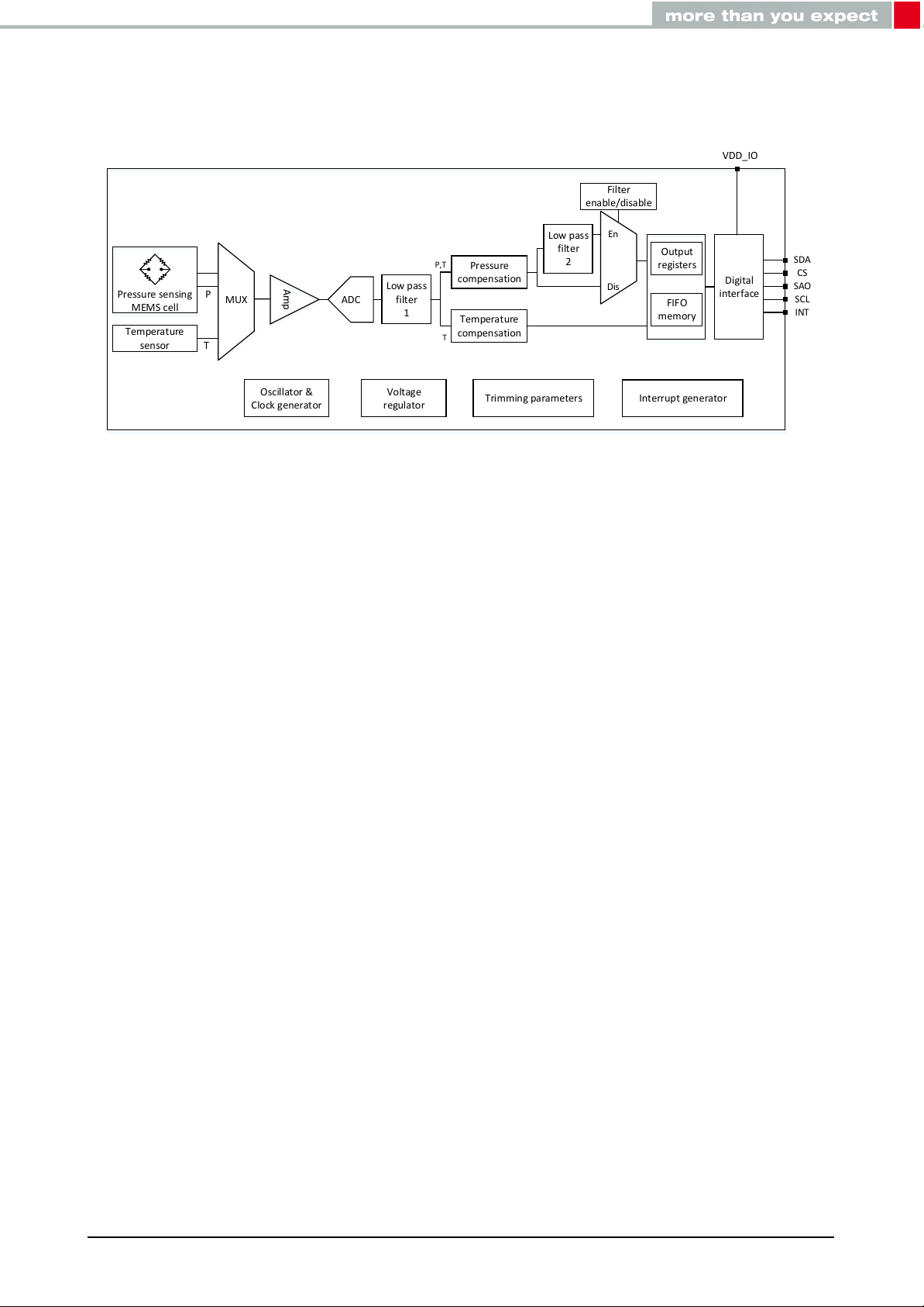
1.4 Block diagram
P,T
Amp
Temperature
sensor
ADC
Pressure
compensation
Temperature
compensation
Low pass
filter
2
Low pass
filter
1
MUX
Output
registers
FIFO
memory
Filter
enable/disable
Digital
interface
En
Dis
Pressure sensing
MEMS cell
SDA
CS
INT
SCL
Oscillator &
Clock generator
Voltage
regulator
Trimming parameters
VDD_IO
P
T
T
SAO
Interrupt generator
Figure 1: Block diagram
1.5 Operational functionality
1.5.1 MEMS Cell
The MEMS cell is the primary pressure sensing element. It contains piezo-resistors embedded on a suspended silicon membrane. The piezo-resistors are connected in a Wheatstone
bridge configuration. When pressure is applied, the membrane is deflected and the bridge
resistance changes. This change leads to a change of the Wheatstone output voltage proportional to the applied pressure. This analog signal is fed to the ASIC.
1.5.2 ASIC
The ASIC comprises of low-noise amplifier, analog-to-digital converter and other signal conditioning blocks that converts an uncompensated analog voltage equivalent to a 24-bit digital
pressure value.
The ASIC embeds a high-resolution temperature sensor which is used for internal compensation of the pressure signal. The temperature information can also be read as a 16-bit
digital value.
1.5.3 Calibration
The sensor is factory calibrated for both pressure and temperature measurements. The
trimming parameters are stored on-chip in the non volatile memory (NVM). Every-time the
sensor is powered on, these trimming parameters are copied from the NVM to the registers.
In normal use, no further calibration is required from the user.
Absolute pressure sensor, Part Nr. 2511020213301
User manual version 2.0 © November2020
www.we-online.com/sensors 8
Page 10
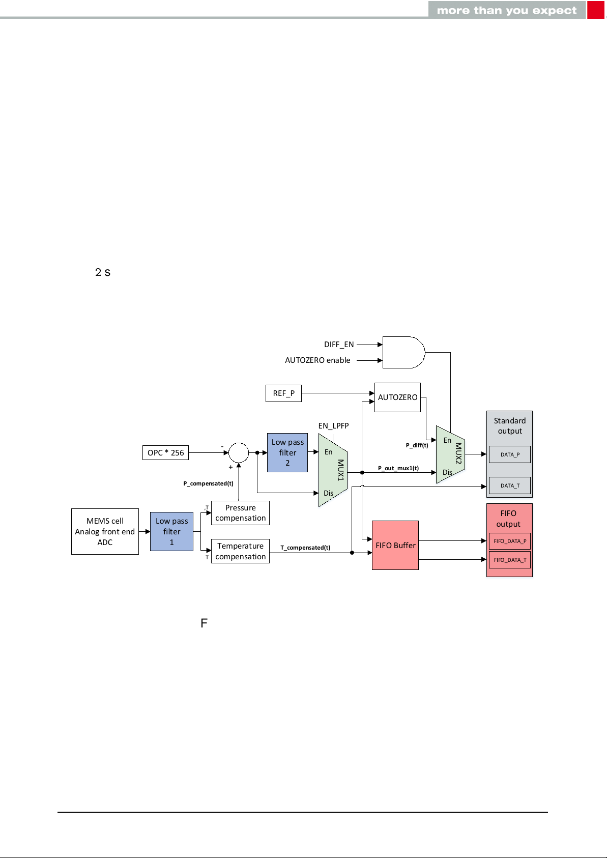
1.5.4 Digital filtering
P,T
Pressure
compensation
Temperature
compensation
Low pass
filter
2
Low pass
filter
1
DATA_P
DATA_T
EN_LPFP
En
Dis
T
MEMS cell
Analog front end
ADC
OPC * 256
-
+
En
Dis
AUTOZERO
REF_P
DIFF_EN
AUTOZERO enable
Standard
output
FIFO Buffer
FIFO_DATA_P
FIFO_DATA_T
FIFO
output
MUX
1
MUX
2
T_compensated(t)
P_compensated(t)
P_out_mux1(t)
P_diff(t)
The sensor has on-chip signal conditioning and embeds two digital low pass filters. The first
filter LPF1 is applied to both pressure and temperature data. The second filter LPF2 can be
optionally applied only to the pressure data. User can turn on or off this filter, depending on
his requirements.
1.5.5 FIFO memory
The sensor has embedded FIFO buffer that can store up to 128 levels of pressure and
temperature data. This can save host controller power, since the controller doesn’t have to
poll for data continuously.
1.6 Filtering chain and data path
Figure2shows detailed information about the functionality of the sensor. The sensor can be
operated in various operating modes and filter setting which determines the pressure and
temperature data path.
Absolute pressure sensor, Part Nr. 2511020213301
User manual version 2.0 © November2020
www.we-online.com/sensors 9
Figure 2: Filtering chain and data path
Page 11
2 Sensor specifications
2.1 General information
Parameter Value
Operating temperature -40 up to +85°C
Storage conditions < 40 °C; < 90% RH
Communication interface I2C
Moisture sensitivity level (MSL) 3
Electrostatic discharge protection (HBM) 2.5 kV
Table 2: General information
2.2 Absolute maximum ratings
Absolute maximum ratings are the limits, the device can be exposed to without causing
permanent damage. Exposure to absolute maximum conditions for extended periods may
affect device reliability.
Parameter Symbol
Input voltage VDD pin V
Input voltage VDD_IO pin V
Input voltage SDA, SCL, CS & SAO pins V
Overpressure P
DD_MAX
DD_IO_MAX
IN_MAX
OVER
Table 3: Absolute maximum ratings
Supply voltage on any pin should never exceed 4.8 V.
The device is susceptible to be damaged by electrostatic discharge (ESD).
Always use proper ESD precautions when handling. Improper handling of the
device can cause performance degradation or permanent damage.
Value
Unit
Min Max
-0.3 4.8 V
-0.3 4.8 V
-0.3 VDD+0.3 V
2 Mpa
Absolute pressure sensor, Part Nr. 2511020213301
User manual version 2.0 © November2020
www.we-online.com/sensors 10
Page 12

2.3 Pressure sensor specification
Unless otherwise stated, all the specified values were measured under the following conditions: T=25°C, VDD=3.3 V.
Parameter
Measurement
range
Absolute
accuracy
1
Relative
accuracy
2
Resolution
Sensitivity
Output data rate
Noise (RMS)
3
Offset change
over temperature
Long term drift
Symbol
Test conditions
Min Typ Max
P
RANGE
P
ACC_ABS
P
ACC_REL
RES
SEN
T= -20 to 80°C ±100 Pa
P= 80 to 110
kPa T= 25°C
P
P
ODR
P
NOISE
P
P
DRIFT
TCO
Low pass filter
enabled
P= 66 to 116 kPa
T= -20 to 65°C
Table 4: Pressure sensor specifications
Value
Unit
26 126 kPa
±2.5 Pa
24 bit
1/40960 kPa/digit
1 200 Hz
0.75
Pa
RMS
±65 Pa/°C
±33 Pa/Year
1. Absolute accuracy includes the soldering drift effects.
2. Typical value is defined based on characterization data with 2kPa interval.
3. Pressure noise RMS is measured in a controlled environment.
2.4 Temperature sensor specification
Parameter
Measurement range
Absolute accuracy
Resolution
Sensitivity
Symbol
Test conditions
Min Typ Max
T
RANGE
T
ACC_ABS
RES
SEN
T= 0 to 80°C ±1.5 °C
T
T
-40 +85 °C
Table 5: Temperature sensor specifications
Value
Unit
16 bit
0.01 °C/digit
Absolute pressure sensor, Part Nr. 2511020213301
User manual version 2.0 © November2020
www.we-online.com/sensors 11
Page 13

2.5 Electrical specifications
Unless otherwise stated, all the specified values were measured under the following conditions: T=25°C, VDD=3.3V.
Parameter
Operating supply
voltage
Supply voltage for I/O
pins
Current consumption in
low power mode
Current consumption in
low noise mode
Current consumption in
power down mode
Digital input voltage high-level
Digital input voltage low-level
Digital output voltage high-level
Symbol
V
DD
V
DD_IO
I
DD_LP
I
DD_LN
I
DD_PD
V
IH
V
IL
V
OH
Test conditions
ODR= 1Hz
ODR= 1Hz
Value
Min Typ Max
1.7 3.3 3.6
1.7 VDD+0.1
4
12
0.9
0.8*V
DD_IO
0.2*V
V
DD_IO
-0.2
DD_IO
Unit
V
V
µA
µA
µA
V
V
V
Digital output voltage low-level
V
IL
Table 6: Electrical specifications
0.2
V
Absolute pressure sensor, Part Nr. 2511020213301
User manual version 2.0 © November2020
www.we-online.com/sensors 12
Page 14
3 Pinning information
VDD_IO
SCL
RSVD
SDA
SAO
CS
INT
GND
GND
VDD
1
2
3
5
6
7
8
10
3.1 Pin configuration
Figure 3: Pin specifications (top view)
3.2 Pin description
Pin
No.
1 VDD_IO
2 SCL I2C/ SPI serial clock Input
3 RSVD Reserved Input Connect to ground
4 SDA
5 SAO
6 CS I2C enable/disable Input High: I2C enable
7 INT Interrupt Input/Output Do not connect if not used
8 GND Negative supply voltage Supply
Name Function I/O Comments
Positive supply voltage
for I/O pins
Supply
Internal pull-up disconnected
by default
I2C serial data; SPI
serial data input
I2C device address
selection; SPI chip
select pin
Input/Output
Input/Output
Internal pull-up disconnected
by default
High: device address LSB is 1
Low: device address LSB is 0
9 GND Negative supply voltage Supply
10 VDD Positive supply voltage Supply
Table 7: Pin description
Absolute pressure sensor, Part Nr. 2511020213301
User manual version 2.0 © November2020
www.we-online.com/sensors 13
Page 15
4 Digital I2C interface
Microcontroller
(Master)
R
p
R
p
Sensor
(Slave-1)
Sensor
(Slave-2)
+VDD
SCL
(serial clock)
SDA
(serial data)
Pull up resistors
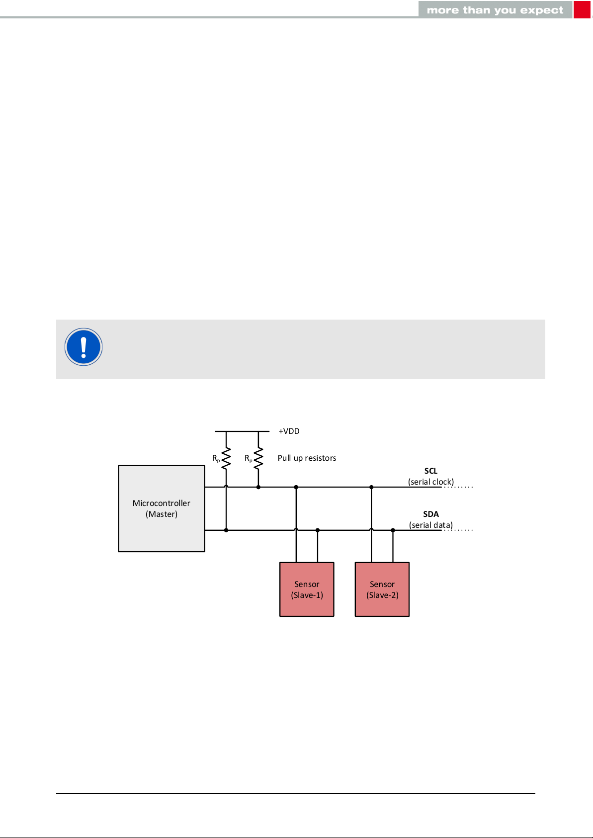
The sensor supports standard I2C (Inter-IC) bus protocol. Further information about the I2C
interface can be found at https://www.nxp.com/docs/en/user-guide/UM10204.pdf. I2C is a
serial 8-bit protocol with two-wire interface that supports communication between different
ICs, for example, between microcontrollers and other peripheral devices.
4.1 General characteristics
A serial data line (SDA) and a serial clock line (SCL) are required for the communication
between the devices connected via I2C bus. Both SDA and SCL lines are bidirectional. The
output stages of devices connected to the bus must have an open-drain or open-collector.
Hence, the SDA and SCL lines are connected to a positive supply voltage via pull-up resistors. In I2C protocol, the communication is realized through master-slave principle. A master
device generates the clock pulse, a start command and a stop command for the data transfer. Each connected device on the bus is addressable via a unique address. Master and
slave can act as a transmitter or a receiver depending upon whether the data needs to be
sent or received.
This sensor behaves like a slave device on the I2C bus
Absolute pressure sensor, Part Nr. 2511020213301
Figure 4: Master-slave concept
User manual version 2.0 © November2020
www.we-online.com/sensors 14
Page 16
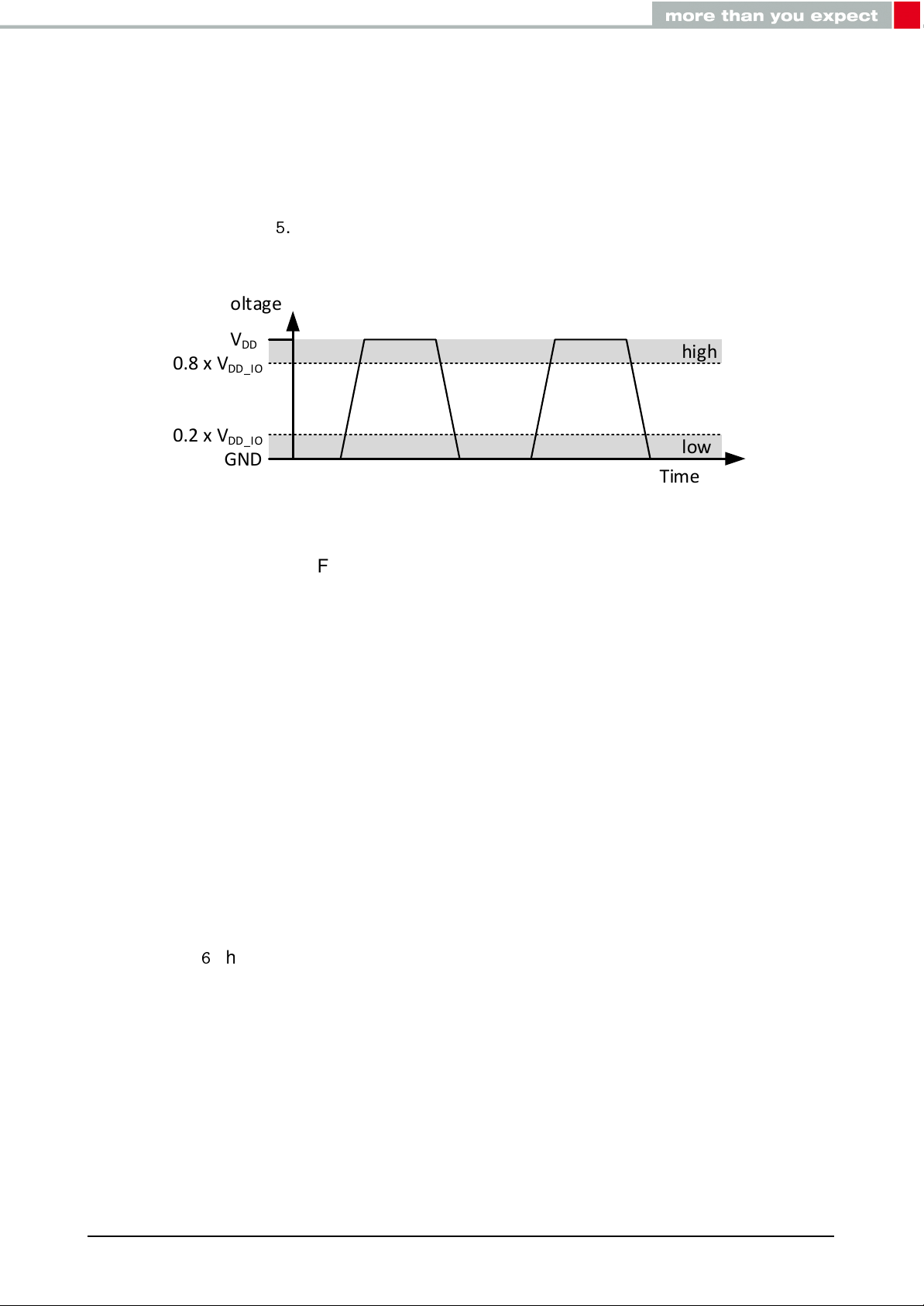
4.2 SDA and SCL logic levels
Voltage
low
high
Time
V
DD
GND
0.2 x V
DD_IO
0.8 x V
DD_IO
The positive supply voltage to which SDA and SCL lines are pulled up (through pull-up
resistors), in turn determines the high level input for the slave devices. The sensor has
separate supply voltage VDD_IO for the SDA and SCL lines. The logic high ’1’ and logic
low ’0’ levels for the SDA and SCL lines then depend on the VDD_IO. Input reference levels
for this sensor are set as 0.8 * VDD_IO (for logic high) and 0.2 * VDD_IO (for logic low).
Explained in the figure5.
Figure 5: SDA and SCL logic levels
4.3 Communication phase
4.3.1 Idle state
During the idle state, the bus is free and both SDA and SCL lines are in logic high ’1’ state.
4.3.2 START(S) and STOP(P) condition
Data transfer on the bus starts with a START command, which is generated by the master.
A start condition is defined as a high-to-low transition on the SDA line while the SCL line is
held high. The bus is considered busy after the start condition.
Data transfer on the bus is terminated with a STOP command, which is also generated by
the master. A low-to-high transition on the SDA line, while the SCL line being high is defined
as a STOP condition. After the stop condition, the bus is again considered free and is in idle
state. Figure6shows the I2C bus START and STOP conditions.
Master can also send a REPEATED START (SR) command instead of STOP command.
REPEATED START condition is the same as the START condition.
Absolute pressure sensor, Part Nr. 2511020213301
User manual version 2.0 © November2020
www.we-online.com/sensors 15
Page 17
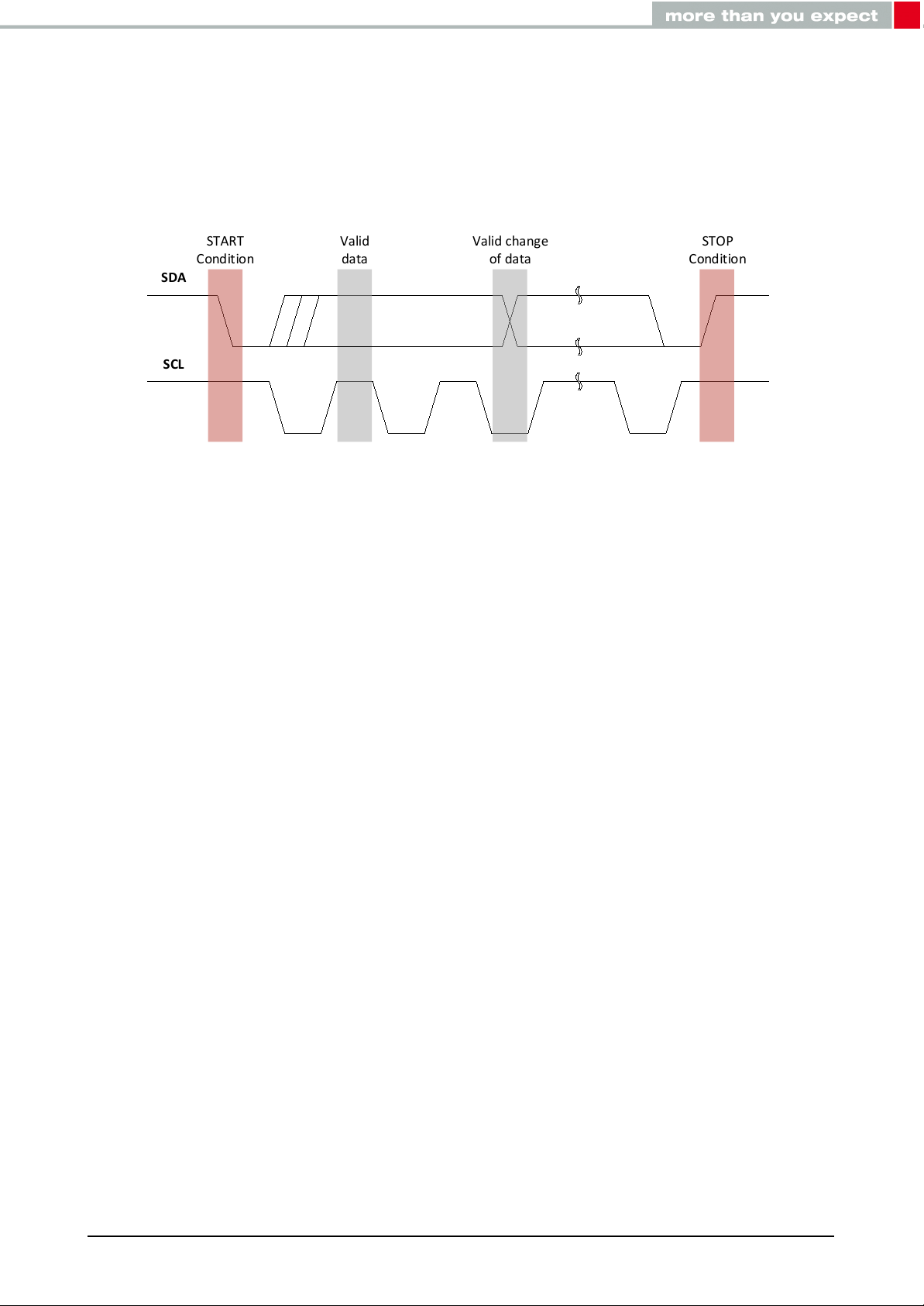
4.3.3 Data validity
SDA
SCL
START
Condition
STOP
Condition
Valid
data
Valid change
of data
After the start condition, one data bit is transferred with each clock pulse. The transmitted
data is only valid when the SDA line data is stable (high or low) during the high period of the
clock pulse. High or low state of the data line can only change when clock pulse is in low
state.
Figure 6: Data validity, START and STOP condition
4.3.4 Byte format
Data transmission on the SDA line is always done in bytes, with each byte being 8-bits long.
Data is transferred with the most significant bit (MSB) followed by other bits.
If the slave cannot receive or transmit another complete byte of data, it can force the master
into a wait state by holding SCL low. Data transfer continues when the slave is ready which
is indicated by releasing the SCL line.
4.3.5 Acknowledge(ACK) and No-Acknowledge(NACK)
Each byte sent on the data line must be followed by an Acknowledge bit. The receiver (master or slave) generates an Acknowledge signal to indicate that the data byte was received
successfully and another data byte could be sent.
After one byte is transmitted, the master generates an additional Acknowledge clock pulse
to continue the data transfer. The transmitter releases the SDA line during this clock pulse
so that the receiver can pull the SDA line to low state in such a way that the SDA line
remains stable low during the entire high period of the clock pulse. This is considered as an
Acknowledge signal.
In case the receiver does not want to receive any further byte, it does not pull down the SDA
line and it remains in stable high state during the entire clock pulse. This is considered as
a No-Acknowledge signal and the master can generate either a stop condition to terminate
the data transfer or a repeated start condition to initiate a new data transfer.
Absolute pressure sensor, Part Nr. 2511020213301
User manual version 2.0 © November2020
www.we-online.com/sensors 16
Page 18
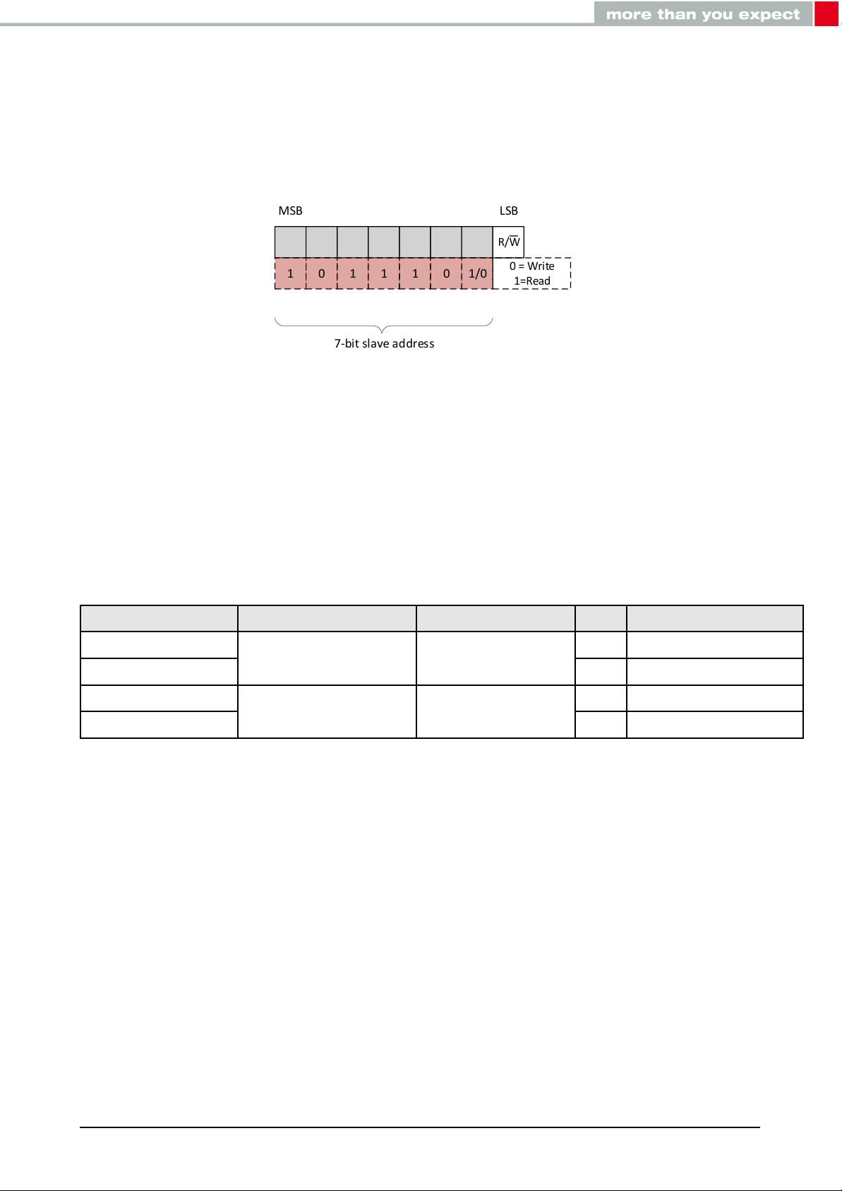
4.3.6 Slave address for the sensor
R/W
7-bit slave address
LSBMSB
1 0 1 1 1 0 1/0
0 = Write
1=Read
The slave address is transmitted after the start condition. Each device on the I2C bus has a
unique address. Master selects the slave by sending corresponding address after the start
condition. A slave address is 7 bits long followed by a Read/Write bit.
Figure 7: Slave address format
The 7-bit slave address for this sensor is 101110xb. LSB of the 7-bit slave address can be
modified with the SAO pin. When SAO is connected to positive supply voltage, the LSB is
’1’, making 7-bit slave address 1011101b (0x5D). If SAO is connected to ground, the LSB is
’0’, making 7-bit address 1011100b (0x5C).
The R/W bit determines the data direction. A ’0’ indicates a write operation (transmission
from master to slave) and a ’1’ indicates a read operation (data request from slave).
Slave address[6:1]
Slave address[0]
7-bit slave address R/W Slave address + R/W
101110 0 10111000b (0xB8)
101110
SAO=0
1011100b (0x5C)
1 10111001b (0xB9)
101110 0 10111010b (0xBA)
101110
SAO=1
1011101b (0x5D)
1 10111011b (0xBB)
Table 8: Slave address and Read/Write commands
Absolute pressure sensor, Part Nr. 2511020213301
User manual version 2.0 © November2020
www.we-online.com/sensors 17
Page 19
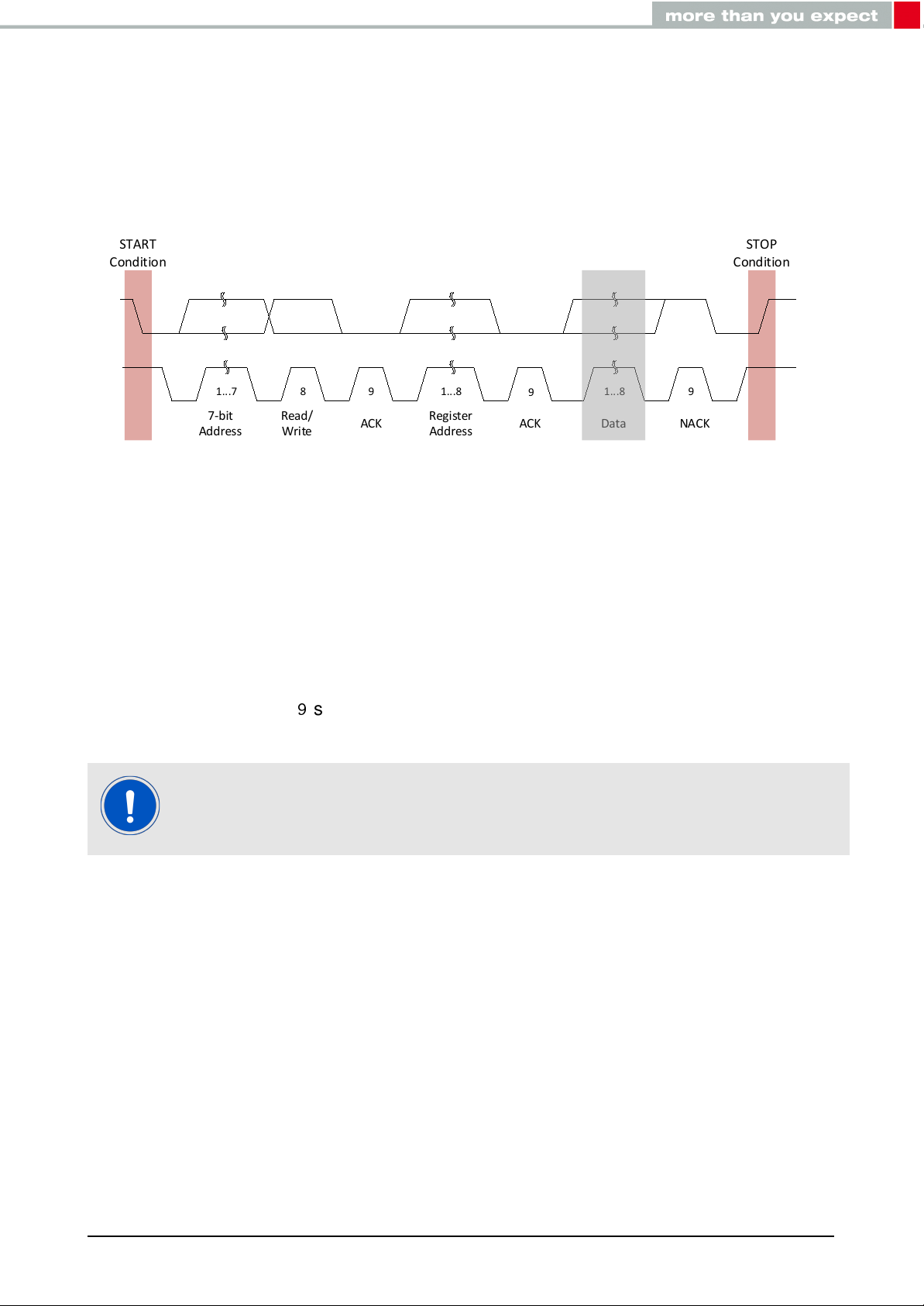
4.3.7 Read/Write operation
START
Condition
STOP
Condition
1...7 8 9 1...8
9
1...8 9
7-bit
Address
Read/
Write
ACK
Register
Address
ACK NACKData
Once the slave-address and data direction bit is sent, the slave acknowledges the master.
The next byte sent by the master must be a register-address of the sensor. This indicates
the address of the register where data needs to be written to or read from.
Figure 8: Complete data transfer
After receiving the register address, the slave sends an Acknowledgement (ACK). If the
master is still writing to the slave (R/W bit = 0), it will transmit the data to slave in the same
direction. If the master wants to read from the addressed register (R/W bit =1), a repeated
start (SR) condition must be sent to the slave. Master acknowledges the slave after receiving
each data byte. If the master no longer wants to receive further data from the slave, it would
send No-Acknowledge (NACK). Afterwards, Master can send a STOP condition to terminate
the data transfer. Figure9shows the writing and reading procedures between the master
and the slave device (sensor).
7-bit slave address of this device is 101110xb. LSB of the 7-bit slave address
depends on the SAO pin
Absolute pressure sensor, Part Nr. 2511020213301
User manual version 2.0 © November2020
www.we-online.com/sensors 18
Page 20
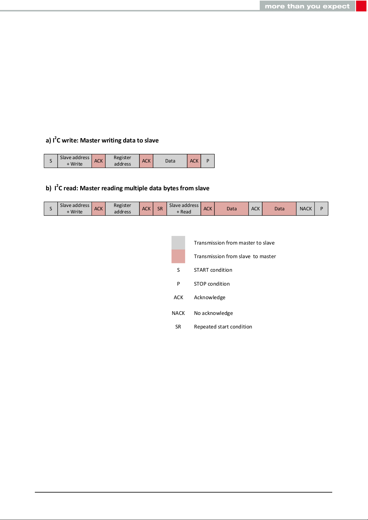
S
Slave address
+ Write
ACK
Register
address
DataACK ACK P
S
Slave address
+ Write
ACK
Register
address
Slave address
+ Read
ACK ACKSR Data Data NACKACK
Transmission from master to slave
Transmission from slave to master
S
P
ACK
NACK
SR
START condition
STOP condition
Acknowledge
No acknowledge
Repeated start condition
a) I2C write: Master writing data to slave
b) I2C read: Master reading multiple data bytes from slave
P
Figure 9: Write and read operations with the device
Absolute pressure sensor, Part Nr. 2511020213301
User manual version 2.0 © November2020
www.we-online.com/sensors 19
Page 21
4.4 I2C timing parameters
Parameter Symbol
Standard mode Fast mode
Unit
Min Max Min Max
SCL clock frequency f
LOW period for SCL clock t
HIGH period for SCL clock t
LOW_SCL
HIGH_SCL
Hold time for START
condition
Setup time for (repeated)
START condition
SDA setup time t
SDA data hold time t
Setup time for STOP
condition
Bus free time between
STOP and START condition
Table 9: I2C timing parameters
SCL
t
HD_S
f
SCL
SU_SDA
HD_SDA
t
SU_P
t
BUF
0 100 0 400 kHz
4.7 1.3 µs
4.0 0.6 µs
4 0.6 µs
4.7 0.6 400 µs
250 100 ns
0 3.45 0 0.9 µs
4 0.6 µs
4.7 1.3 µs
Absolute pressure sensor, Part Nr. 2511020213301
User manual version 2.0 © November2020
www.we-online.com/sensors 20
Page 22
5 Serial Peripheral Interface (SPI)
µC
(SPI Master)
Sensor
(SPI Slave)
MOSI
MISO
CLK
CS
SDA
SAO
CLK
CS
Serial Peripheral Interface (SPI) is a synchronous serial communication bus system for the
communication between host microcontroller and other peripheral ICs such as ADCs, EEPROMs, sensors, etc. SPI is a full-duplex master-slave based interface allowing the communication to happen in both directions simultaneously. The data from the master or the slave
is synchronized either on the rising or falling edge of clock pulse. SPI can be either 4-wire or
3-wire interface. 4-wire interface consists of two signal lines and two data lines. All of these
bus lines are unidiretional.
1. Clock (SCL)
2. Chip select (CS)
3. Master out, slave in (MOSI)
4. Master in, slave out (MISO)
Figure 10: SPI Interface
Master generates the clock signal and is connected to all slave devices. Data transmission
between the master and salves is synchronized to the clock signal generated by the master.
One master can be connected to one or more slave devices. Each slave device is addressed
and controlled by the master via individual chip select (CS) signals. CS is controlled by the
master and is normally an active low signal.
MOSI and MISO are data lines. MOSI transmits data from the master to the slave. MISO
transmits data from the slave to the master.
This sensor supports both 3-wire and 4-wire SPI.
Absolute pressure sensor, Part Nr. 2511020213301
User manual version 2.0 © November2020
www.we-online.com/sensors 21
Page 23
5.1 Data transfer
Communication begins when the master selects a slave device by pulling the CS line to
LOW. The clock and data lines (MOSI/MISO) are available for the selected slave device.
Data stored in the specific shift registers are exchanged synchronously between master and
the slave through MISO and MOSI lines. The data transmission is over when the chip select
line is pulled up to the HIGH state. 4-wire SPI uses both data lines for the synchronous data
exchange in both the direction. 3-wire SPI shares a single data line for the data transfer,
where the master and slave alternate their transmitter and receiver roles synchronously.
5.2 Communcation modes
In SPI, the master can select the clock polarity (CPOL) and clock phase (CPHA). The CPOL
bit sets the polarity of the clock signal during the idle state. The CPHA bit selects the clock
phase. Depending on the CPHA bit, the rising or falling clock edge is used to sample and
shift the data. Depending on the CPOL and CPHA bit selection in the SPI control registers,
four SPI modes are available as per table10. In order to ensure proper communication,
master and the slave must be set to same communication modes.
CPOL CPHA Desription
0 0 Clock polarity LOW in idle state; Data sampled on the rising clock edge
0 1 Clock polarity LOW in idle state; Data sampled on the falling clock edge
1 1 Clock polarity HIGH in idle state; Data sampled on the falling clock edge
1 0 Clock polarity HIGH in idle state; Data sampled on the rising clock edge
Table 10: SPI communication modes
Absolute pressure sensor, Part Nr. 2511020213301
User manual version 2.0 © November2020
www.we-online.com/sensors 22
Page 24
5.3 Sensor SPI Communcation
7- bit register address
R/W
LSBMSB
A[6]
A[5] A[4] A[3] A[2] A[1] A[0]
0 = Write
1=Read
R/W A[6] A[5] A[4] A[3] A[2] A[1] A[0] DI[7] DI[6] DI[5] DI[4] DI[3] DI[2] DI[1] DI[0]
DO[7] DO[6] DO[5] DO[4] DO[3] DO[2] DO[1] DO[0]
CS
SCK
SDA
SAO
4-Wire SPI of this sensor uses following lines: SDA (data input, MOSI), SAO (data output,
MISO), SCL (serial clock) and CS (chip select). For more information, please refer to pin
description in the section
CS is pulled LOW by the master at the start of communication. The SCL polarity is HIGH in
the idle state (CPOL = 1). The data lines (SDA & SAO) are sampled at the falling clock edge
and latched at the rising clock edge (CPHA = 1). Data is transmitted with MSB first and the
LSB last.
SPI read and write operations are completed in 2 or more bytes (multiple of 16 or more clock
pulses). Each block consits of a register address byte and a data byte. The first byte is the
register address. In the SPI communication, the register address is specified in the 7-bits
and the the MSB of the register address is used as an SPI read/write bit (Figure11). When
R/W is ’0’, the data is written on to the sensor. When ’1’, the data is read from the sensor.
3.2
Figure 11: SPI register address
The next bytes of data, depending on the R/W bit, is either written to or read from the indexed
register. Figure12shows the complete SPI data transfer protocol.
The sensor also supports 3-wire SPI communication. SDA is used for both
data read and write operations. Communication protocol remains the same.
Figure 12: 4-wire SPI data transfer (CPOL = 1, CPHA = 1)
Absolute pressure sensor, Part Nr. 2511020213301
User manual version 2.0 © November2020
www.we-online.com/sensors 23
Page 25
5.3.1 SPI write operation
Register address
A[6]
A[5] A[4] A[3] A[2] A[1] A[0]
R/WStart
CS =
LOW
0
DI
[6]
DI
[5]
DI
[4]
DI
[3]
DI
[2]
DI
[1]
DI
[0]
DI
[7]
Data to be written
Stop
CS =
HIGH
Register address
A[6] A[5] A[4] A[3] A[2] A[1] A[0]
R/WStart
CS =
LOW
1
DO
[6]
DO
[5]
DO
[4]
DO
[3]
DO
[7]
DO
[7]
DO
[7]
DO
[7]
Data from indexed register
Stop
CS =
HIGH
The write operation starts with the CS = LOW and sending the 7-bit register address with
R/W bit = ’0’ (write command). Next byte is the data byte that is the data to be written to the
indexed register. Several write command pairs can be sent without raising the CS back to
HIGH. The operation is ended with CS = HIGH. The SPI write protocol is shown in the figure
13
.
Figure 13: SPI write protocol
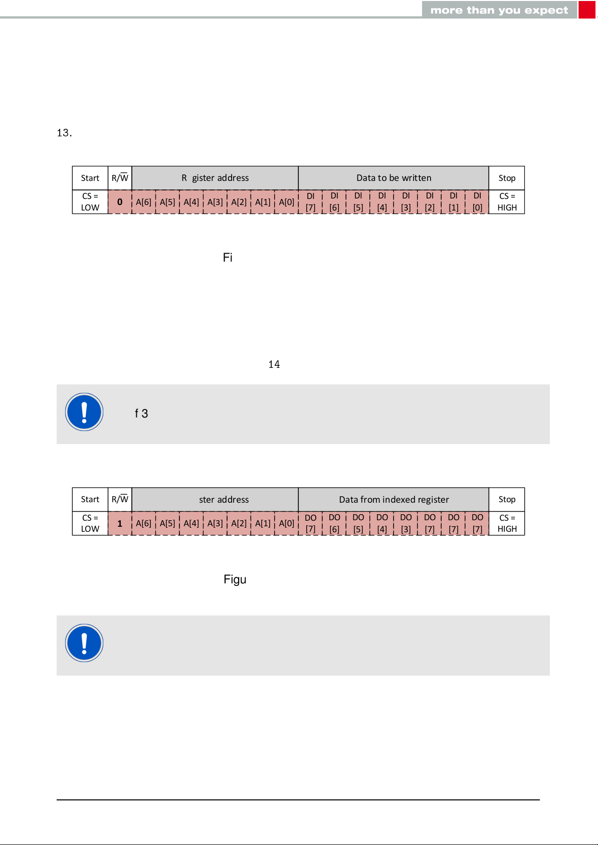
5.3.2 SPI read operation
The read operation starts with the CS = LOW and sending the 7-bit register address with
R/W bit = ’1’ (read command). Data is sent out from the sensor through the SAO line. The
SPI read protocol is shown in the figure14.
If 3-wire SPI is used, the data is sent out through the SDA line.
Figure 14: SPI read protocol
During multiple read/write operation, the register address is automatically incremented after each block. This feature is enabled by default with the bit
IF_ADD_INC set to ’1’ in the CTRL_2 register.
Absolute pressure sensor, Part Nr. 2511020213301
User manual version 2.0 © November2020
www.we-online.com/sensors 24
Page 26
3-wire SPI can be enabled by setting bit SIM to ’1’ in the CTRL_1 register.
5.3.3 SPI timing parameters
Table11shows general SPI timing parameters. They are subject to VDD and the operating
temperature.
Parameter Symbol Min Max Unit
SCL clock frequency f
SCL
10
(1)
MHz
SPI clock cycle t
CS setup time t
CS hold time t
SDA input setup time t
SDA input hold time t
SAO valid output time t
SAO output hold time t
SAO output disable time t
SCL
SU_CS
h_CS
SU_SDA
h_SDA
v_SAO
h_SAO
dis_SAO
Table 11: SPI timing parameters
1. Recommended maximum SPI clock frequency for ODR ≤ 50 Hz is 8 MHz
100 ns
6 ns
6 ns
5 ns
15 ns
50 ns
9 ns
50 ns
Absolute pressure sensor, Part Nr. 2511020213301
User manual version 2.0 © November2020
www.we-online.com/sensors 25
Page 27
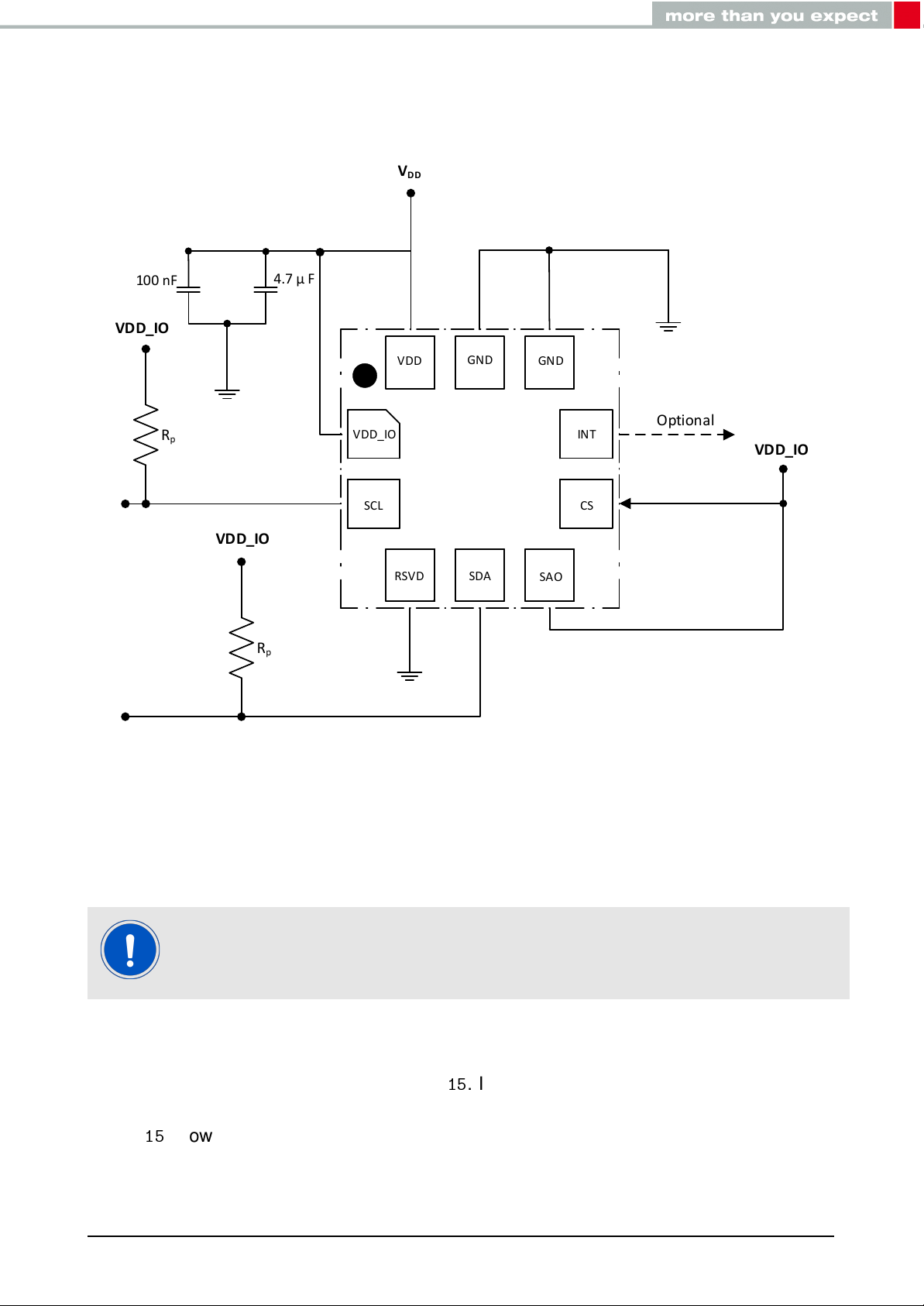
6 Application circuit
VDD_IO
SCL
SDA
RSVD
SAO
CS
INT
GND
VDD
GND
R
p
R
p
V
DD
VDD_IO
VDD_IO
VDD_IO
Optional
100 nF
4.7 µ F
Figure 15: Application circuit with I2C interface (top view)
The sensor has two separate supply pins: VDD and VDD_IO. VDD pin is the central supply pin for the MEMS cell and internal circuits. VDD_IO provides the supply to the digital
interface.
VDD_IO voltage level must be equal to or lower than VDD+0.1 V.
In order to prevent ripple from the power supply, a decoupling capacitor of 100 nF must be
placed as close to the VDD pad of the sensor as possible. An optional decoupling capacitor
(4.7 µF) could placed as shown in the figure15. If VDD_IO is not connected to the VDD line,
a separate decoupling capacitor of 10nF should be added on the VDD_IO line.
Figure15shows a typical application circuit for I2C communication. For proper I2C functionality, the CS pin must be connected to VDD. Least significant bit of the 7-bit slave address
Absolute pressure sensor, Part Nr. 2511020213301
User manual version 2.0 © November2020
www.we-online.com/sensors 26
Page 28

can be modified based on the status of the SAO pin. In order to optimize the power consumption, it is recommended to connect SAO pin to VDD (SAO = 1) if only one sensor is
used on the I2C line. This sets the 7 bit slave address as 0x5D (1011101b). SCL and SDA
must be connected to VDD_IO through the pull-up resistors. Proper value of the pull-up
resistors must be chosen depending on the I2C bus speed and load.
Pins SDA and SCL have internal pull up resistors. By default they are disabled and can
be enabled through bits SDA_PU_EN and SAO_PU_EN in InNTERFACE_CTRL register
(0x0E). Value of the internal pull up varies between 30kΩ 50kΩ, depending on VDD_IO.
Sensor communication with the master controller remains active even if VDD is disconnected
while VDD_IO is maintained. However, in this situation, the internal measurement cycle is
turned off.
Absolute pressure sensor, Part Nr. 2511020213301
User manual version 2.0 © November2020
www.we-online.com/sensors 27
Page 29

7 Quick start guide
BOOT_ON bit
VDD_IO
VDD
power off
power
on
boot process
4.5 ms (max)
sensor ready for
communication
Time [s]
BOOT_ON bit = '1' ;
self cleared when boot ends
7.1 Power-up sequence
The sensor is powered up when supply voltage is applied to VDD and VDD_IO pins. During the power up sequence, it is recommended to keep the I2C interface pins in the high
impedance state from the host controller side.
During the power up sequence of the sensor, the sensor performs a boot process. During
this process, trimming parameters and calibration coefficients are loaded to the internal
registers from the embedded non-volatile memory. The booting process lasts for a maximum
of 4.5 milliseconds. During this period, the internal registers are not accessible to read or
write the data. However, the status of the boot procedure can be checked by reading the
BOOT bit in the INT_SOURCE register (0x24). This bit is set to ’1’ during the boot procedure
and automatically goes back to ’0’ once it has ended. At the end of the power-up sequence
the sensor automatically enters into power-down mode and is ready for data measurements.
Figure 16: Power-up sequence
Absolute pressure sensor, Part Nr. 2511020213301
User manual version 2.0 © November2020
www.we-online.com/sensors 28
Page 30

7.2 Communication with host controller
Power up
Wait for
4.5 ms
Device Id=
0xB3 ?
Read DEVICE_ID register
Address: 0x0F
Communication
successfull
No communication
with the device
Yes
No
No Yes
Communication with the host controller via I2C interface can be checked by reading the
DEVICE_ID register (0x0F). Device ID for this sensor is 0xB3.
Figure 17: Communication check with host controller
7.3 Reboot
Reboot procedure can be also performed by the user in case the trimming parameters are
somehow modified during operations. The Reboot procedure restores the correct values
and resets the offset calibration registers OPC_L (0x18) and OPC_H (0x19) to ’0’
When the BOOT bit in the CTRL_2 register (0x11) is set to ’1’, the trimming parameters are
copied to the corresponding internal registers and are used to calibrate the device. At the
end of the reboot process the BOOT bit is self cleared to ’0’.
Status of the reboot procedure can be checked by the BOOT_ON bit as mentioned in the
section
7.1
7.4 Software reset
To set the internal registers to the default values, software reset can be performed. It is done
by setting the SWRESET bit in the CTRL_2 register (0x11) to ’1’. Following registers are
reset to their default values during the software reset.
• INTERRUPT_CFG (0x0B)
• THR_P_L (0x0C)
Absolute pressure sensor, Part Nr. 2511020213301
User manual version 2.0 © November2020
www.we-online.com/sensors 29
Page 31

• THR_P_H (0x0C)
BOOT bit
BOOT_ON bit
SWRESET bit
Boot process
4.5 ms (max)
SW reset
50µs
Time [s]
• INTERFACE_CTRL (0x0E)
• CTRL_1 (0x10)
• CTRL_2 (0x11)
• CTRL_3 (0x12)
• FIFO_CTRL (0x13)
• FIFO_WTM (0x14)
• INT_SOURCE (0x24)
• FIFO_STATUS1 (0x25)
• FIFO_STATUS2 (0x26)
• STATUS (0x27)
The software reset procedure lasts for a maximum of 50 µs. At the end of the software reset,
the SWRESET bit in CTRL_2 register (0x11) is automatically set back to ’0’.
The reboot and software reset procedure must not be executed simultaneously. Both processes can be executed serially as shown in Figure
18
Figure 18: Reboot and software reset sequence
Absolute pressure sensor, Part Nr. 2511020213301
User manual version 2.0 © November2020
www.we-online.com/sensors 30
Do not set BOOT and SWRESET bits to ’1’ at the same time.
Page 32

7.5 Sensor operation: single conversion mode
Power-down
mode
Read pressure and temperature
data registers (0x28 – 0x2C)
No
Yes
Set bit ONE_SHOT=‘1‘
in CTRL_2 register (0x11)
Power-down
mode
Trigger one set of data conversion by
setting ONE_SHOT bit to '1'
(Automatic increment register
address enabled by default)
Get pressure and temperature
values in SI unit
Combine corresponding data
registers and multiply with the
sensitivity parameter; SENP= 1/
40960; SENT=0.01
New set of data?
Flow chart shows sensor operation in the single conversion mode.
Figure 19: Sensor operation: single-conversion mode
Absolute pressure sensor, Part Nr. 2511020213301
User manual version 2.0 © November2020
www.we-online.com/sensors 31
Page 33

7.6 Sensor operation: continuous mode
Power-down mode
Read pressure and temperature data
registers (0x28 – 0x2C)
Set sensor in continuous mode with ODR = 50Hz;
Get pressure and temperature
values in SI unit
Combine corresponding data registers and multiply
with the sensitivity parameter; SENP= 1/40960;
SENT=0.01
Set bit LOW_NOISE_ENABLE= ‘1‘
in CTRL_2 register (0x11)
Enable Low-noise configuration
(Automatic increment register address enabled by
default)
Set bits ODR[2:0]= ‘100‘
in CTRL_1 register (0x10)
Wait t=1/ODR
Set bits EN_LPFP= ‘1‘, LPFP_CFG=‘1‘
and BDU= ‘1‘
in CTRL_1 register (0x10)
Additional low pass filter enabled & BW=ODR/20 ;
Enable block data update
Flow chart shows sensor operation in continuous mode with 50Hz ODR and low-noise configuration enabled.
Figure 20: Sensor operation: continuous mode
Absolute pressure sensor, Part Nr. 2511020213301
User manual version 2.0 © November2020
www.we-online.com/sensors 32
Page 34

7.7 Power-off sequence
VDD rise/fall time for the sensor varies between 10 µs and 100 ms. For proper device power
off, it is recommended to drive the VDD pin to GND or less than 0.2 V and keep it stable at
this level for at least 10 ms.
This procedure is also necessary to guarantee the next power-on and boot procedure to be
successful.
Absolute pressure sensor, Part Nr. 2511020213301
User manual version 2.0 © November2020
www.we-online.com/sensors 33
Page 35

8 Modes of operation
Power off
VDD & VDD_IO applied
Single Conversion mode
One measurement
Continuous mode
Periodic measurements as per
selected ODR
Power on
&
Boot process
Power-down mode
ODR[2:0] ≠ '000'
ODR[2:0] = '000'
ONE_SHOT = '1'
The sensor can be configured to be used in the following 3 different modes.
1. Power-down mode
2. Single conversion mode
3. Continuous mode
Additionally, the device can be operated in either low-power or low-noise configuration. Transition to/from one of the operating modes and configurations can be executed by writing to
specific registers.
Absolute pressure sensor, Part Nr. 2511020213301
User manual version 2.0 © November2020
www.we-online.com/sensors 34
Figure 21: Operating modes
Page 36

8.1 Power-down mode
The power-down mode can be configured by setting the ODR[2:0] bits of CTRL_1 register
(0x10) to ’000’.
In power-down mode the digital chain that samples the pressure and temperature values is
turned off. No new measurement is performed during this mode. Hence, the data registers
containing pressure and temperature values are not updated. The data registers contain the
last sampled pressure and temperature data before going into power-down mode. Current
consumption is at the minimum during this mode.
However, serial communication with the host controller via I2C bus is still possible. This
allows the user to configure the device by accessing the configuration/control registers. Data
of the control registers remains unaffected when the sensor is configured to power-down
mode from another mode.
Sensor is in power-down mode by default after the power-up sequence.
Absolute pressure sensor, Part Nr. 2511020213301
User manual version 2.0 © November2020
www.we-online.com/sensors 35
Page 37

8.2 Single conversion mode
Pressure
data
Temperature
data
Time [s]
1
st
Measurement
2
nd
Measurement
3
rd
Measurement
P P P T T P P P T T P P P T T
Power down
mode
ONE_SHOT bit =1
Measurement
in progress
In this mode single measurement of pressure and temperature is performed according to
the request of the host controller. This mode can be activated only when the sensor is in
the power-down mode. When ONE_SHOT bit of CTRL_2 register (0x11) is set to ’1’, the
digital chain is turned on, data conversion starts and a single measurement of pressure and
temperature is acquired. This measurement data is written in the respective pressure and
temperature data registers. Afterwards, the digital chain is turned off again and the sensor
enters the power-down mode. The ONE_SHOT bit of CTRL_2 register (0x11) automatically
returns to ’0’ (default value). The data registers are not updated until another data acquisition
is requested by the host controller. This mode is useful when the application demands
reduced power consumption.
During this mode the output data rate (ODR) of new measurement depends on the new
measurement request from the host controller (frequency at which the ONE_SHOT bit is set
to ’1’).
Figure 22: Single conversion mode
Figure12shows typical data conversion time in low-power and low-noise configuration.
Configuration Conversion time [ms]
Low-power 4.7
Low-noise 13.2
Table 12: Data conversion time
Absolute pressure sensor, Part Nr. 2511020213301
User manual version 2.0 © November2020
www.we-online.com/sensors 36
Page 38

8.3 Continuous mode
Pressure
data
Temperature
data
t=1/ODR
Time [s]
1
st
Measurement
2
nd
Measurement
3
rd
Measurement
t=1/ODR t=1/ODR
P P P T T P P P T T P P P T T
The sensor is configured in the continuous mode when the ODR[2:0] bits of CTR_1 register
(0x10) are set to a value other than ’000’. The continuous mode constantly samples new
pressure and temperature measurements and writes the data to the corresponding data
registers. The measurement rate is defined by the user selectable output data rate (ODR)
which can be set by ODR[2:0] bits of CTRL_1 register. Selectable ODR and corresponding
register settings are shown in the table
13
Figure 23: Continuous mode
ODR[2:0] Output data rate [Hz]
000 Power-down mode / One-shot mode
001 1
010 10
011 25
100 50
101 75
110 100
111 200
Table 13: Output data rate selection
Absolute pressure sensor, Part Nr. 2511020213301
User manual version 2.0 © November2020
www.we-online.com/sensors 37
Page 39

8.4 Additional configurations
During continuous mode and single conversion mode, additional configurations can be selected. These include enabling the additional low pass filter; selecting either low-power or
low-noise configuration.
8.4.1 Low-power or low-noise configuration
In the low-power configuration, the device is configured to minimize the current consumption.
In the low-noise configuration, the device is configured to reduce the noise. During the
continuous mode and single conversion mode, either one of these configurations can be
selected as shown in Table14. By default the sensor operates in the low-power configuration.
Address Register Bit Bit value Configuration
0x11 CTRL_2 LOW_NOISE_EN 0 Low-power (default)
0x11 CTRL_2 LOW_NOISE_EN 1 Low-noise
Table 14: Low-power/low-noise configuration
To ensure the proper behaviour of the device, LOW_NOISE_EN bit must
changed only when it is in the power-down mode.
Table
mode.
15
shows typical conversion time and maximum allowable ODR in each operating
Maximum ODR [Hz]
Configuration
Low-power 4.7 200 200
Low-noise 13.2 50 75
Low-noise configuration is not available at ODR 100 Hz or 200Hz. If ODR is
set to 100Hz or 200Hz, LOW_NOISE_EN bit must be set to ’0’.
Typical data conversion time
[ms]
Table 15: Typical conversion time and maximum ODR
Single
conversion mode
Continuous
mode
Absolute pressure sensor, Part Nr. 2511020213301
User manual version 2.0 © November2020
www.we-online.com/sensors 38
Page 40

8.4.2 Enabling additional low-pass filter
The sensor embeds two digital low-pass filters. First low-pass filter LPF1 is always applied
to the pressure and temperature data. The second low-pass filter LPF2 can be optionally
enabled and applied to the pressure data. This configuration is available for both continuous
mode and single conversion mode.
The second low-pass filter LPF2 can be enabled by setting the EN_LPFP bit in the CTRL_1
register (0x10) to ’1’. Further, overall device bandwidth can also be configured by changing
LPFP_CFG bit of the CTRL_1 (0x10) register. LPF2 is applied only to the pressure data.
EN_LPFP LPFP_CFG LPF2 status Device Bandwidth
0 x Disabled/reset filter ODR/2
1 0 Enabled ODR/9
1 1 Enabled ODR/20
Samples to be
discarded
0
2
2
Table 16: Additional low-pass filter setting
When EN_LPF bit in the CTRL_1 (0x10) is changed from ’1’ to ’0’, the filter is reset. The
filter is also reset when the ODR or device bandwidth is changed. Table
16
indicates the
number of samples to be discarded when the filter is enabled or reset. The output data is
not considered meaningful before the filter reaches the settling condition.
Absolute pressure sensor, Part Nr. 2511020213301
User manual version 2.0 © November2020
www.we-online.com/sensors 39
Page 41

9 Reading output data
Once the device is configured in one of the operating modes, pressure and temperature
values are sampled and stored in the respective data registers, available for the user to
read.
It is recommended to read the data registers starting from the lower address
to the higher address.
9.1 Reading pressure values
Pressure values are stored in the three data registers: DATA_P_XL, DATA_P_L and DA-
TA_P_H. Each register contains 8-bits data. The complete pressure data is represented as
a 24-bit signed 2’s complement word. This can be obtained by concatenating the three 8-bit
pressure data registers: DATA_P_H, DATA_P_L & DATA_P_XL, with DATA_P_H being most
significant byte and DATA_P_XL being least significant byte.
After calculating the 24-bit digital pressure value, it must be multiplied with the sensitivity
parameter, SENP(see table4) in order to obtain the corresponding pressure in SI unit (Pa).
Step 1: Reading raw data from the three pressure data registers
1. DATA_P_XL (0x28)
2. DATA_P_L (0x29)
3. DATA_P_H (0x2A)
Step 2: Concatenating pressure data registers to obtain complete 24-bit pressure value
P
= DATA_P_H & DATA_P_L & DATA_P_XL
24bit
Step 3: Obtaining pressure value in SI unit (Pa) by multiplying with sensitivity parameter
Pressure [Pa] = P
24bit
[digit] ×
1
40960
[Pa/digit]
Example:
If values obtained from pressure data registers are:
DATA_P_XL = 0x00
DATA_P_L = 0x54
DATA_P_H = 0x3F
Concatenating these 3 registers (0x3F5400) to obtain 24-bit signed decimal value and multiplying with the sensitivity parameter
P
[digit] = 4150272 [digit]
24bit
P[kPa] = 4150272 [digit] * 1/40960 [kPa/digit] = 101.325 kPa
Absolute pressure sensor, Part Nr. 2511020213301
User manual version 2.0 © November2020
www.we-online.com/sensors 40
Page 42

9.2 Reading temperature values
Temperature values are stored in the two data registers: DATA_T_L and DATA_P_H. Each
register contains 8-bits data. The complete temperature data is a 16-bit signed 2’s complement word. This can be obtained by concatenating the two 8-bit temperature data registers:
DATA_T_H & DATA_P_L, with DATA_T_H being most significant byte and DATA_T_L being
least significant byte.
After calculating the 16-bit digital temperature value, it must be multiplied with the sensitivity
parameter, SENT(see table5) in order to obtain the corresponding temperature in SI unit
(°C).
Step 1: Reading raw data from the two temperature data registers
1. DATA_T_L (0x2B)
2. DATA_T_H (0x2C)
Step 2: Concatenating the temperature data registers to obtain complete 16-bit temperature
value
T
= DATA_T_H & DATA_T_L
16bit
Step 3: Obtaining temperature value in SI unit [°C] by multiplying with sensitivity parameter
Temperature [°C] = T
[digit] ×0.01 [°C/digit]
16bit
Example:
If values obtained from temperature data registers are:
DATA_T_L = 0x42
DATA_T_H = 0x0E
Concatenating these 2 registers (0x0E42)to obtain 16-bit signed decimal value and multiplying with sensitivity parameter
T
[digit] = 3650 [digit]
16bit
T[°C] = 3650 [digit] * 0.01 [°C/digit] = 36.50 °C
Absolute pressure sensor, Part Nr. 2511020213301
User manual version 2.0 © November2020
www.we-online.com/sensors 41
Page 43

9.3 Status register for reading the data
Pressure sample
Pressure
data
P_DA
P_OR
Data read
Previous measurement
overwritten
DATA_P_H is read
The sensor has a STATUS register (0x27) that can be used to check when a new set of
pressure or temperature data is available in the corresponding data register.
P_DA bit is set to ’1’ whenever a new sample is available in the pressure data registers.
P_DA bit is self cleared and set back to ’0’ when the corresponding pressure data (most
significant byte, DATA_P_H) has been read.
Same way, T_DA bit is set to ’1’ whenever a new set of data is available in the temperature data registers. T_DA bit is self cleared and set back to ’0’ when the corresponding
temperature data (Most significant byte, DATA_T_H) has been read.
Bits P_OR and T_OR of the STATUS register (0x27) are overrun flags for pressure and
temperature data respectively. Whenever a previous pressure or temperature sample in the
data register is overwritten without being read by the user, P_OR and T_OR bits are set to
’1’, indicating that previous value has been lost. P_OR and T_OR bit will be set to ’1’ in case
a new pressure or temperature data is measured while the corresponding x_DA bit is still ’1’.
They are automatically set to ’0’ when all data from the corresponding data registers have
been read and no new measurement is generated in the meantime.
Figure 24: Reading pressure data using STATUS register
Since, pressure and temperature data are synchronously generated, P_DA and T_DA synchronously rises to ’1’ (unless one of the bit is already one). However, they would not synchronously reset to ’0’ as it depends on when the corresponding data is read.
Reading the data registers (pressure and temperature) before 1/ODR time period allows acquisition of all data and resetting P_DA and T_DA before the
overrun flags are set.
If the sensor is configured in the single conversion mode, the STATUS register
will not be updated after the first measurement because the sensor goes to
power down mode after the first acquisition.
Absolute pressure sensor, Part Nr. 2511020213301
User manual version 2.0 © November2020
www.we-online.com/sensors 42
Page 44

10 FIFO buffer
The sensor has an embedded first-in, first-out (FIFO) buffer that can store upto 128 sets of
pressure and temperature data. Each data set consists of 5 bytes of data (3 bytes pressure
and 2 bytes temperature). This allows considerable power saving of the system because
the host controller does not have to continuously poll for new data from the sensor. The
host controller can be notified via the INT pin when it is required to read the data from FIFO
buffer. FIFO events can be used to generate interrupt via INT pin.
FIFO can be operated in six different user selectable modes.
• Bypass mode
• FIFO mode
• Continuous mode
• Bypass-to-FIFO mode
• Bypass-to-continuous mode
• Continuous-to-FIFO mode
Figure 25: First-In-First-Out buffer
FIFO behaves as a circular buffer. The buffer is filled with new data set (pressure and
temperature) in the first available empty slot. Once the buffer is full, FIFO either stops filling
the new data sets or the oldest data set is replaced by the new data sets.
Absolute pressure sensor, Part Nr. 2511020213301
User manual version 2.0 © November2020
www.we-online.com/sensors 43
Page 45

When FIFO is enabled, pressure and temperature data is sent to the FIFO buffer at the
selected ODR in the CTRL_1 register. The host controller can read the data stored in FIFO buffer. The oldest data set is always read first. FIFO modes can be configured from
FIFO_CTRL register. (0x13).
FIFO_CTRL [2:0]
TRIG_MODE F_MODE[1] F_MODE[0]
x 0 0 Bypass mode
0 0 1 FIFO mode
0 1 x Continuous mode
1 0 1 Bypass-to-FIFO mode
1 1 0 Bypass-to-Continuous mode
1 1 1 Continuous-to-FIFO mode
Table 17: FIFO mode settings
FIFO Mode
Absolute pressure sensor, Part Nr. 2511020213301
User manual version 2.0 © November2020
www.we-online.com/sensors 44
Page 46

10.1 Bypass mode
FIFO buffer is not in operation in the bypass mode. By default the FIFO buffer is in bypass
mode and FIFO remains empty. Each new data set is directly available in the respective
data (DATA_P_x, DATA_T_x) registers (See Figure26)
The device can be configured in the bypass mode by writing ’000’ or ’100’ to register FIFO_CTRL[2:0].
Enabling bypass mode clears the FIFO buffer and must be used while switching
between other FIFO modes.
Figure 26: Bypass mode
Absolute pressure sensor, Part Nr. 2511020213301
User manual version 2.0 © November2020
www.we-online.com/sensors 45
Page 47

10.2 FIFO mode
This mode is enabled by settings bits [2:0] of FIFO_CTRL (0x13) to ’001’.
In this mode, each data set (pressure and temperature) is stored in the FIFO buffer at se-
lected ODR. The FIFO buffer keeps filling untill it is full or reaches the user-defined FIFO
threshold (see section
FSS[7:0] bits in FIFO_STATUS_1 register (0x25) shows the number of data sets stored in
FIFO buffer. This register is updated every 1/ODR period.
Once the FIFO is full, bit FIFO_FULL_IA or FIFO_WTM_IA (if user defined FIFO threshold
level is enabled) in the FIFO_STATUS_2 register (0x26) will be set to ’1’, and buffer stops
storing new data sets. At this point data in the FIFO buffer will remain unchanged and
further measured data sets will be lost. Data stored in FIFO buffer can be read from five
FIFO_DATA_x_x registers(0x78-0x7C). See section (see section
10.7.1
).
10.7.2
)
Figure 27: FIFO mode
In order to fill the FIFO buffer with new sets of measurement data, the device
must be first configured in the bypass mode to reset the FIFO buffer and then
again in the FIFO mode.
Absolute pressure sensor, Part Nr. 2511020213301
User manual version 2.0 © November2020
www.we-online.com/sensors 46
Page 48

10.3 Continuous mode
This mode is enabled by settings bits [2:0] of FIFO_CTRL (0x13) to ’010’ or ’011’.
In this mode, each data set (pressure and temperature) is stored in the FIFO buffer at se-
lected ODR. Once the FIFO buffer is full or reaches the user-defined FIFO threshold, oldest
data sets will be overwritten by the new data sets, meaning older data sets will be lost.
FSS[7:0] bits in FIFO_STATUS_1 register (0x25) indicate the number of data sets stored in
FIFO buffer. This register is updated every 1/ODR period.
Once the FIFO is full, bit FIFO_FULL_IA or FIFO_WTM_IA (if user defined FIFO threshold
level is enabled) in the FIFO_STATUS_2 register (0x26) will be set to ’1’. At this point, older
data sets are replaced by new data sets and FIFO_OVR_IA bit in the FIFO_STATUS_2
register (0x26) goes to ’1’, indicating that at least one data set has been overwritten.
Figure 28: Continuous mode
If FIFO buffer is overwritten without a read operation, bits FIFO_FULL_IA and
FIFO_WTM_IA are set back to ’0’ after the first data set is overwritten.
New data sets will continue to overwrite the old data sets until a read operation is initiated
by the host controller or the FIFO is reset. In order to avoid losing the older data sets, data
must be read faster than the ODR. Host controller can be alerted about FIFO full or FIFO
overwritten event by routing the status of FIFO_FULL_IA, FIFO_WTM_IA or FIFO_OVR_IA
to the INT pin of the device through corresponding bits of CTRL_3 register (0x12).
Absolute pressure sensor, Part Nr. 2511020213301
User manual version 2.0 © November2020
www.we-online.com/sensors 47
Page 49

10.4 Bypass-to-FIFO mode
This mode is enabled by settings bits [2:0] of FIFO_CTRL (0x13) to ’101’.
In this mode, initially FIFO buffer is in bypass mode. When an interrupt trigger event is
generated, FIFO switches from bypass mode to FIFO mode and starts filling the slots with
measurement data sets until the buffer is full.
Switching from the bypass mode to the FIFO mode can be triggered by an interrupt event
selected by user through INT_CFG (0x0B) register. The selected event generation leads IA
bit of INT_SOURCE (0x24) register to rise to ’1’. When this bit rises to ’1’ for the first time,
the buffer switches to FIFO mode.
When the IA bit goes back to ’0’, FIFO does not switch back to bypass mode.
Absolute pressure sensor, Part Nr. 2511020213301
User manual version 2.0 © November2020
www.we-online.com/sensors 48
Page 50

10.5 Bypass-to-continuous mode
This mode is enabled by settings bits [2:0] of FIFO_CTRL (0x13) to ’110’.
In this mode, initially FIFO buffer is in bypass mode. When an interrupt trigger event is
generated, FIFO switches from bypass mode to continuous mode and starts filling the slots
with measurement data sets; once FIFO is full, it will overwrite old data sets with the new
data.
Switching from the bypass mode to the continuous mode can be triggered by an interrupt
event selected by the user through INT_CFG (0x0B) register. The selected event generation
leads IA bit of INT_SOURCE (0x24) register to rise to ’1’. When this bit rises to ’1’ for the
first time, FIFO switches to continuous mode.
Figure 29: Bypass-to-Continuous mode
When the IA bit goes back to ’0’, FIFO does not switch back to bypass mode.
Absolute pressure sensor, Part Nr. 2511020213301
User manual version 2.0 © November2020
www.we-online.com/sensors 49
Page 51

10.6 Continuous-to-FIFO mode
This mode is enabled by settings bits [2:0] of FIFO_CTRL (0x13) to ’111’.
In this mode, initially FIFO buffer is in continuous mode. When an interrupt trigger event is
generated, FIFO switches from continuous mode to FIFO mode and continues to fill the slots
with the data sets; once FIFO is full, it will stop storing the data in the FIFO buffer.
Switching from continuous to FIFO mode can be triggered by an interrupt event selected by
the user through INT_CFG (0x0B) register. The selected event generation leads IA bit of
INT_SOURCE (0x24) register to rise to ’1’. When this bit rises to ’1’ for the first time, the
buffer switches to FIFO mode.
Figure 30: Continuous-to-FIFO mode
When the IA bit goes back to ’0’, FIFO does not switch back to continuous
mode.
Absolute pressure sensor, Part Nr. 2511020213301
User manual version 2.0 © November2020
www.we-online.com/sensors 50
Page 52

10.7 FIFO status monitoring and control
When FIFO is in operation, its status can be monitored by reading two registers, FIFO_STATUS_1
(0x25) and FIFO_STATUS_2 (0x26).
FIFO_STATUS_1 register shows the current number of data sets stored in the FIFO buffer.
0000000b indicates FIFO is empty and 1000000b indicates FIFO is full with 128 data sets.
FIFO_STATUS_2 register has 3 FIFO buffer flags.
• FIFO_WTM_IA flag indicates when FIFO buffer is equal to or higher than user defined
FIFO threshold level (only if this feature is enabled through FIFO_CTRL register). The
status of this flag can be routed to INT pad of the sensor via CTRL_3 register by setting
INT_F_WTM bit to ’1’.
• FIFO_OVER_IA flag indicates when FIFO is full and at least one data set is overwritten
with a new one. The status of this flag can be routed to INT pad of the sensor via
CTRL_3 register by setting INT_F_OVR bit to ’1’.
• FIFO_FULL_IA flag indicates when FIFO is completely filled with 128 data sets. The
status of this flag can be routed to INT pad of the sensor via CTRL_3 register by setting
INT_F_FULL bit to ’1’.
Absolute pressure sensor, Part Nr. 2511020213301
User manual version 2.0 © November2020
www.we-online.com/sensors 51
Page 53

10.7.1 User-defined FIFO threshold
Normally, FIFO can be filled with 128 sets of data. However, user can limit the FIFO buffer
depth with FIFO_WTM (0x14) register. The user can define the required FIFO threshold
level by setting bits WTM[6:0] of FIFO_WTM registers to the corresponding value. Maximum
allowable value in this register is 0x7F.
The user-defined FIFO threshold has to be enabled by setting STOP_ON_WTM bit of FI-
FO_CTRL (0x13) register to ’1’. When enabled, the FIFO level size will be considered as
the value defined im the FIFO_WTM register.
User-defined FIFO threshold level can not be changed when FIFO is already
in operation.
10.7.2 Reading data from FIFO buffer
When FIFO buffer is in operation, the data stored in FIFO is available to read from dedicated FIFO data registers. Pressure values can be read from FIFO_P_x (0x78 to 0x7A) and
temperature values can be read from FIFO_T_x (0x7B to 0x7C) registers. Every time a data
set is read, remaining oldest entry in the FIFO buffer is placed in the FIFO data registers,
available to be read. FIFO status registers FIFO_STATUS_1 (0x0x25) and FIFO_STATUS_2
(0x0x26) are also updated accordingly.
FIFO data registers (0x78-0x7C) can be read with multi read/write feature which is enabled
by default. Number of read operations can be determined based on the number of data sets
stored in the FIFO buffer. The current number of data sets stored in the FIFO buffer can be
known by reading FIFO_STATUS_1 (0x0x25) register.
If differential interrupt is enabled (bit DIFF_EN = ’1’) with AUTOZERO mode (bit
AUTOZERO = ’1’), then FIFO buffer will contain values other than the standard
pressure data registers.
Absolute pressure sensor, Part Nr. 2511020213301
User manual version 2.0 © November2020
www.we-online.com/sensors 52
Page 54

11 Interrupt functionality
The sensor has a dedicated interrupt generator which generates various interrupt events.
The interrupt events can be monitored via dedicated status registers. Available interrupt
events and their dedicated status registers are listed below.
• Pressure data ready event (STATUS register (0x27))
• Based on pressure threshold (INT_SOURCE register (0x24))
– Pressure high
– Pressure low
– Pressure high or low
• FIFO status (FIFO_STATUS_2 register (0x26))
– FIFO full
– FIFO overrun
– FIFO threshold
11.1 Interrupt generation on pressure data-ready
It is possible to generate a hardware signal through the INT pin of the sensor when a new
set of measurement data is available. This feature can be used to trigger an external action
synchronously as soon as a new set of data is available.
As mentioned in the section
new set of pressure data is generated. This can be routed to the INT pin of the device by
setting bit DRDY = 1 and INT_S[1:0] = 00 of CTRL_3 register (0x12).
P_DA bit and the data-ready signal on INT resets after the most significant byte of pressure
data is read.
Data-ready interrupt generation is only available for pressure data.
9.3
, P_DA bit in the STATUS register goes to ’1’, whenever a
Absolute pressure sensor, Part Nr. 2511020213301
User manual version 2.0 © November2020
www.we-online.com/sensors 53
Page 55

11.2 Interrupt generation based on pressure threshold
Differential pressure
Pressure threshold
Pressure threshold
REF_P
-
+
P_out_mux1
Interrupt can be generated on the differential pressure signal when DIFF_EN bit is set to ’1’.
When differential pressure is above or below user-defined threshold pressure, an interrupt
signal on the INT pin can be generated.
Figure 31: Differential pressure interrupt
DIFF_EN is used with either AUTOZERO or AUTOREFP configuration. When one of these
configuration is enabled, the measured pressure is automatically stored in the REF_P (0x150x16) as a 16-bit signed value.
Measured pressure is a 3-byte long signed value, but REF_P contains the 2
most significant bytes of the measured pressure value
If AUTOZERO mode is engaged, the pressure data registers DATA_P_x (0x28-0x2A) are updated with the difference between the measured pressure and REF_P value. The differential
pressure value is also updated with the difference between the measured pressure and REF_P value. During AUTOZERO configuration, DATA_P_x registers contain the differential
pressure value and not the standard absolute pressure value.
• Differential pressure = measured pressured-REF_P
• Data_P_x = measured pressure-REF_P
To obtain the absolute pressure in kPa from the DATA_P_x registers in the
AUTOZERO configuration, the DATA_P_x[digits] has to be divided by a factor
of 160 [digits/kPa]
Bit AUTOZERO is set back to ’0’ after the first conversion but the configuration still remains
active. To disable, bit RESET_AZ needs to be set to ’1’. RESET_AZ bit is set back to ’0’
automatically. This resets the REF_P registers to default value ’0’ and the pressure data
registers DATA_P_x show default pressure data.
Absolute pressure sensor, Part Nr. 2511020213301
User manual version 2.0 © November2020
www.we-online.com/sensors 54
Page 56

If AUTOREFP mode is engaged, the pressure data registers DATA_P_x (0x28-0x2A) will
contain the measured pressured but the the differential pressure value will still be updated
with the difference between the measured pressured and REF_P value.
• Differential pressure = measured pressured-REF_P
• Data_P_x = measured pressure
Bit AUTOREFP is set back to ’0’ after the first conversion but the configuration still remains
active. To disable, bit RESET_ARP needs to be set to ’1’. RESET_AZ bit is set back to ’0’
automatically. This resets the REF_P registers to default value ’0’.
Figure 32: Interrupt generation with AUTOZERO enabled
Absolute pressure sensor, Part Nr. 2511020213301
User manual version 2.0 © November2020
www.we-online.com/sensors 55
Page 57

The sensor has dedicated pressure threshold registers THR_P_L and THR_P_H, where
user-defined pressure can be stored as a 15 bit unsigned value. Desired pressure threshold
value can be stored in the THR_P_x registers as shown below.
Pressure threshold [digit] =
Pressure threshold [kPa]
SENP[kPa/digit] ×256 [kPa/digit]
SENP= 1/40960 [kPa/digit]
Example:
If the pressure threshold for the interrupt is 10 kPa.
Pressure threshold = 10 [kPa] / (256/40960) [kPa/digit] = 1600 [digits]
Threshold pressure value is 0x0640
THR_P_L = 0x40
THR_P_H = 0x06
User defined pressure threshold is a 15-bit unsigned value which represents a
differential pressure and not absolute pressure value.
When, bits PHE = ’1’ or PLE = ’1’ or both are set to ’1’, the differential pressure is compared
to the user defined pressure value at each new sample generation and an interrupt signal is
generated accordingly. Based on the status of the PHE and PLE bits, interrupt signals can
be generated on the INT pin of the sensor.
PHE PLE Interrupt Event
1 0 Differential pressure is above the THR_P value (+THR)
0 1 Differential pressure is below the THR_P value (-THR)
1 1 Differential pressure is above or below the THR_P vlaue
Table 18: Interrupt based on pressure threshold
To enable the differential pressure interrupt with AUTOZERO configuration, bits
AUTOZERO, DIFF_EN, PLE and/or PHE have to be set to ’1’.
To enable the differential pressure interrupt with AUTOZERO configuration, bits
AUTOZERO, DIFF_EN, PLE and/or PHE have to be set to ’1’.
Absolute pressure sensor, Part Nr. 2511020213301
User manual version 2.0 © November2020
www.we-online.com/sensors 56
Page 58

11.2.1 Interrupt latching
+ THR_P
- THR_P
Time [s]
IA bit
PH bit
PL bit
INT_SOURCE is read
IA and PH are latched to high state
even if pre ssure is below +THR_P
level
INT pin
Differential
pressure
IA bit
PH bit
PL bit
INT pin
IA bit is not latched and is not
effected by INT_SOURCE read
operation
Interrupt latch enabled
Interrupt latch disabled
The interrupt generated based on the pressure threshold, can be also latched. Interrupt
flags (PH, PL or IA) in the INT_SOURCE registers can be latched to their ’high’ states, even
if the condition that triggered their rise is not valid anymore. The interrupt flags only get reset
when INT_SOURCE (0x24) register has been read.
Interrupt latching is enabled by setting LIR bit of INT_CFG (0x0B) register to ’1’. In this case,
when the IA bit rises to ’1’ it will remain in the same state until the INT_SOURCE is read.
Interrupt latching is also routed to the INT pin of the sensor if IA or PH or PL flags are routed
to generate an interrupt.
Figure 33: Interrupt latching
Absolute pressure sensor, Part Nr. 2511020213301
User manual version 2.0 © November2020
www.we-online.com/sensors 57
Page 59

11.3 FIFO status based interrupt events
When FIFO is active, interrupt event can be generated based on the status of FIFO registers. Status of FIFO registers can be checked from FIFO_STATUS_2 (0x26) register. By
configuring the CTRL_3 register, it is possible to route the event to the INT pin.
Bit
INT_F_FULL
INT_F_WTM
INT_F_OVR
FIFO modes can also be triggered from the interrupt events. When the bit IA in the IN-
T_SOURCE register 0x24 is set to ’1’, following FIFO buffer mode can be triggered.
• Bypass-to-FIFO mode (when FIFO_CTRL bits [2:0] are set to ’101’)
• Bypass-to-Continuous mode (when FIFO_CTRL bits [2:0] are set to ’110’)
• Continuous-to-FIFO mode (when FIFO_CTRL bits [2:0] are set to ’111’)
Bit value Event
1 FIFO is full
1 User-defined FIFO threshold level is reached
1 FIFO is full and at least one measurement is overwritten
Table 19: FIFO interrupts
11.4 Routing interrupt events to the INT pin
All the interrupt events can be individually selected and routed to the INT pin of the sensor
from CTRL_3 register.
Interrupt Event Routing to INT pin
Pressure data ready Bit DRDY = ’1’ and bits INT_S[1:0] = ’00’
FIFO full Bit INT_F_FULL = ’1’ and bits INT_S[1:0] = ’00’
FIFO Overrun Bit INT_F_OVR = ’1’ and bits INT_S[1:0] = ’00’
FIFO threshold Bit INT_F_WTM = ’1’ and bits INT_S[1:0] = ’00’
Pressure high or low Bit PLE or PHE= ’1’ and bits INT_S[1:0] = ’11’
Pressure high Bit PLE= ’1’ and bits INT_S[1:0] = ’01’
Pressure low Bit PLE= ’1’ and bits INT_S[1:0] = ’10’
Table 20: Routing interrupt events to INT pin
It is also possible to route multiple interrupt events to the INT. The interrupt events are
connected via logical OR operation and multiplexed to the INT pin (see figure34). To know
which interrupt event triggered the interrupt signal on INT pin, the corresponding status
registers have to be read.
Absolute pressure sensor, Part Nr. 2511020213301
User manual version 2.0 © November2020
www.we-online.com/sensors 58
Page 60

CTRL_3 (0x12) Register
DRDY
INT_F_WTM
INT_F_OVR
INT_F_FULL
OR
OR
Pressure high
Pressure low
INT pin
00
01
10
11
INT_S[1:0]
Figure 34: Routing interrupt events to INT pin
INT_S[1] INT_S[0]
0 0
0 1 Pressure high event
1 0 Pressure low event
1 1 Pressure low or high event
Absolute pressure sensor, Part Nr. 2511020213301
User manual version 2.0 © November2020
www.we-online.com/sensors 59
INT pin configuration
Data signal (priority order: DRDY or INT_F_WTM or
INT_F_OVER or INT_F_FULL)
Table 21: INT pin configuration
Page 61

12 Register map
Addr. Register Name Type
0x0B INT_CFG R/W
0x0C THR_P_L R/W
0x0D THR_P_H R/W
0x0E INTERFACE_CTRL R/W 0 0 0
0x0F DEVICE_ID R 1 0 1 1 0 0 1 1 Device ID register
0x10 CTRL_1 R/W 0
0x11 CTRL_2 R/W BOOT INT_H_L PP_OD
0x12 CTRL_3 R/W 0 0
0x13 FIFO_CTRL R/W 0 0 0 0
0x14 FIFO_WTM R/W 0
0x15 REF_P_L R
0x16 REF_P_H R
0x18 OPC_P_L R/W
0x19 OPC_P_H R/W
0x1A-
0x23
0x24 INT_SOURCE R
0x25 FIFO_STATUS_1 R
0x26 FIFO_STATUS_2 R
0x27 STATUS R 0 0 T_OR P_OR 0 0 T_DA P_DA Status register
0x28 DATA_P_XL R
0x29 DATA_P_L R
0x2A DATA_P_H R
0x2B DATA_T_L R
0x2C DATA_T_H R
0x2D-
0x77
0x78 FIFO_DATA_P_XL R
0x79 FIFO_DATA_P_L R
0x7A FIFO_DATA_P_H R
0x7B FIFO_DATA_T_L R
0x7C FIFO_DATA_T_H R
Reserved
Reserved
7 6 5 4 3 2 1 0
AUTO
REFP
BOOT_
ON
FIFO_
WTM_IA
RESET_
ARP
FIFO_
OVR_IA
AUTO
ZERO
ODR[2:0]
INT_F_
FULL
0 0 0 0 IA PL PH Interrupt register
FIFO_
FULL_IA
Bits
RESET_AZDIFF_
SDA_
PU_EN
IF_ADD_
INC
INT_F_
WTM
0 0 0 0 0
DATA_P[7:0]
DATA_P[15:8]
DATA_P[23:16]
DATA_T[7:0]
DATA_T[15:8]
FIFO_P[7:0]
FIFO_P[15:8]
FIFO_P[23:15]
FIFO_T[7:0]
FIFO_P[15:8]
THR[7:0]
THR[15:8]
ON_WTM
WTM[6:0]
REFL[7:0]
REFH[15:8]
OPCP[7:0]
OPCP[15:8]
-
FSS[7:0]
-
EN
SAO_
PU_EN
EN_
LPFP
0
INT_F_
OVR
STOP_
LIR PLE PHE
PD_
DIS_INT
LPFP_
CFG
SW
RESET
DRDY
TRIG_
MODES
0
BDU SIM Control register-1
LOW_
NOISE_
ENABLE
INT_S[1:0]
F_MODE[1:0]
I2C_
DIS-
ABLE
ONE_
SHOT
Comments
Interrupt
configuration register
Pressure threshold
register
Interface control
register
Control register-2
Control register-3
FIFO control register
FIFO threshold level
Reference pressure
register
Reference pressure
register
Reserved
FIFO status registers
Pressure output
registers
Temperature output
registers
Reserved
Pressure output
registers
Temperature output
registers
Writing to reserved registers may cause permanent damage to the device.
Register addresses not listed in the above table, must not be accessed and
content must not be modified.
Register contents that are loaded during the boot process should not be
changed. They contain factory calibration values and their content is automatically restored at the power up.
Absolute pressure sensor, Part Nr. 2511020213301
User manual version 2.0 © November2020
www.we-online.com/sensors 60
Page 62

13 Register description
13.1 INT_CFG (0x0B)
Address: 0x0B
Type: R/W
Default Value: 00000000b
7 6 5 4 3 2 1 0
AUTO
REFP
RESET_
ARP
AUTO
ZERO
RESET_
AZ
DIFF_EN LIR PLE PHE
AUTOREFP Enable AUTOREFP function. Measured pressure value is stored
in REF_P_x registers (0x15-0x16). Pressure data registers, DATA_P_x show actual measured values
0: AUTOREFP is disabled 1: AUTOREFP is enabled
RESET_ARP Reset AUTOREFP function. Resets REF_P_x register values
0: normal mode 1: reset AUTOREFP
AUTOZERO Enable AUTOZERO mode. Measured pressure value is stored in
REF_P_x registers (0x15-0x16) and used as reference for measured data. Pressure data registers DATA_P_x contain the difference between measured pressure and REF_P registers.
0: AUTOZERO is disabled 1: AUTOZERO is enabled
RESET_AZ Reset AUTOZERO function; Resets REF_P_x register values
0: normal mode 1: reset AUTOZERO
DIFF_EN Enable differential interrupt generation. To be used with AUTOREFP
and AUTOZERO mode
0: differential interrupt disabled; 1: differential interrupt is enabled
LIR Interrupt request is latched to the INT_SOURCE register (0x24)
0: interrupt is not latched; 1: interrupt is latched
PLE Enable differential pressure interrupt generation when pressure val-
ue is lower than the user-defined threshold value set in register
THR_P_x (0x0c-0x0D)
0: interrupt is inactive; 1: interrupt active on pressure low event
Absolute pressure sensor, Part Nr. 2511020213301
User manual version 2.0 © November2020
www.we-online.com/sensors 61
Page 63

PHE Enable differential pressure interrupt generation when pressure val-
ue is higher than the user-defined threshold value set in register
THR_P_x (0x0c-0x0D)
0: interrupt is inactive; 1: interrupt active on pressure high event
AUTOZERO or AUTOREFP mode must be enabled when differential pressure
interrupt is desired.
AUTOZERO and AUTOREFP bits are set back to ’0’ after the first measurement and two most significant bytes of the measured value are stored in RE-
F_P_H and REF_P_L registers. In order to return to normal mode, RESET_AZ
or RESET_ARP must be set to ’1’.
Absolute pressure sensor, Part Nr. 2511020213301
User manual version 2.0 © November2020
www.we-online.com/sensors 62
Page 64

13.2 THR_P_L (0x0C)
Address: 0x0C
Type: R/W
Default Value: 00000000b
7 6 5 4 3 2 1 0
THR[7:0]
THR[7:0] LSB of the user defined pressure threshold value to generate a pres-
sure based interrupt event.
13.3 THR_P_H (0x0D)
Address: 0x0D
Type: R/W
Default Value: 00000000b
7 6 5 4 3 2 1 0
-
THR[15:8] MSB of the user defined pressure threshold value to generate a
pressure based interrupt event.
User-defined pressure threshold value is expressed in 15-bit unsigned right-justified value
stored in THR_P_H and THR_P_L registers. It can be calculated as follows:
Pressure threshold value (kPa) ×16 = THR_P[15:0]
THR_P value is a differential pressure threshold and not absolute pressure
threshold.
THR[14:8]
Enable interrupt based on user-defined pressure threshold
1. Set DIFF_EN bit to ’1’ in INT_CFG register (0x0B)
2. Set PHE or PLE (or both) = ’1’, based on the user application
Absolute pressure sensor, Part Nr. 2511020213301
User manual version 2.0 © November2020
www.we-online.com/sensors 63
Page 65

13.4 INTERFACE_CTRL (0x0E)
Address: 0x0E
Type: R/W
Default Value: 00000000b
7 6 5 4 3 2 1 0
0 0 0
SDA_PU_EN Enable internal pull-up resistors on the SDA pin
0: internal pull-up not connected; 1: internal pull-up is connected
SAO_PU_EN Enable internal pull-up resistors on the SAO pin
0: internal pull-up not connected; 1: internal pull-up is connected
PD_DIS_INT Disable internal pull-down on INT pin
0: INT pin pull-down connected; 1: INT pin pull-down is disconnected
I2C_DISABLE Disable I2C digital interface
0: I2C enabled; 1: I2C disabled
SDA_PU
_EN
SAO_PU
_EN
PD_DIS
_INT
I2C_
0
DIS-
ABLE
13.5 DEVICE_ID (0x0F)
Address: 0x0F
Type: R
Default Value: 10110011b (0xB3)
7 6 5 4 3 2 1 0
1 0 1 1 0 0 1 1
Device ID for this device is a fixed number (0xB3) which is stored in this register.
Absolute pressure sensor, Part Nr. 2511020213301
User manual version 2.0 © November2020
www.we-online.com/sensors 64
Page 66

13.6 CTRL_1 (0x10)
Address: 0x10
Type: R/W
Default Value: 00000000b
7 6 5 4 3 2 1 0
0
ODR[2:0] Selection of operating mode and ODR as per table
ODR[2:0] Output Data Rate [Hz]
000 Power-down mode / single-conversion mode
001 1
010 10
011 25
100 50
101 75
110 100
111 200
EN_LPFP Enable/disable Low-pass filter. For more information refer to section
ODR[2:0]
Table 22: Output data rate selection
8.4.2
EN_
LPFP
LPFP_
CFG
BDU SIM
22
0: low-pass filter is disabled; 1: low-pass filter is enabled
LPFP_CFG Configure low-pass filter. For more information refer to section
BDU Block data update feature
0: data register updates continuously; 1: data register not updated
until MSB and LSB has been read
SIM SPI interface mode selection
0: 4-wire interface; 1: 3-wire interface
BDU: Block data update feature
While reading the output data, this feature can be enabled to inhibit the values of data
registers to be updated until all bytes of the pressure or temperature data registers have
been read.
8.4.2
Absolute pressure sensor, Part Nr. 2511020213301
User manual version 2.0 © November2020
www.we-online.com/sensors 65
Page 67

This feature should be enabled when the reading of the data is slower than the output data
rate (ODR). By default, the BDU bit is set to ’0’ and data registers are updated continuously.
When BDU feature is enabled, reading of the pressure or temperature values sampled at
different times can be avoided.
For example, when reading of the register DATA_P_XL is initialized, the remaining part of
the pressure data registers DATA_P_L and DATA_P_H are not updated until all three bytes
(XL, L and H) have been read. In case of temperature data readout, if DATA_T_L is read
than the value of DATA_T_H will not be updated until read.
It is strongly recommended to enable BDU feature. This avoids an update of
the DATA_x_x registers until all the parts of the corresponding DATA_x registers
have been read.
13.7 CTRL_2 (0x11)
Address: 0x11
Type: R/W
Default Value: 00010000b (0x10)
7 6 5 4 3 2 1 0
BOOT INT_H_L PP_OD
BOOT Reboots memory content. For details refer to section
0: normal operation; 1: reboot memory content
INT_H_L Select interrupt: active high or active low
0: active high; 1: active low
PP_OD Push-pull or open-drain selection on the INT pin
0: push-pull; 1: open-drain
IF_ADD_INC Register address is automatically incremented during multiple byte
access
0: disabled; 1: enabled
This is a multi-read/write feature that enables a repeated read/write
operation during a single bus transaction by automatically incrementing the register address. This feature is enabled by default.
IF_ADD_
INC
0
SW
RESET
LOW_
NOISE_
EN
7.3
ONE_
SHOT
SWRESET Perform a software reset. For more information, refer to section
0: Normal operation; 1: software reset
Absolute pressure sensor, Part Nr. 2511020213301
User manual version 2.0 © November2020
www.we-online.com/sensors 66
7.4
Page 68

LOW_NOISE_
ENABLE
ONE_SHOT Enables single data acquisition of pressure and temperature. For
Enable low-noise or low-power configuration. For more information
refer to section
0: low-power mode; 1: low-noise mode
more information refer to section
0: normal operation; 1: a new data set is acquired
8.4.1
8.2
13.8 CTRL_3 (0x12)
Address: 0x12
Type: R/W
Default Value: 00000000b
7 6 5 4 3 2 1 0
0 0
INT_F_FULL FIFO full status (128 unread samples) is routed to INT pin
INT_F_WTM User defined FIFO threshold full status is routed to INT pin
INT_F_OVR FIFO overrun status is routed to INT pin
DRDY Data-ready signal routed to INT pin
INT_S[1:0] Interrupt event control on INT pin. Refer to table
INT_F_
FULL
0: disabled; 1: FIFO full interrupt enabled
0: disabled; 1: FIFO threshold level interrupt enabled
0: disabled; 1: FIFO overrun interrupt enabled
0: disabled; 1: enabled
INT_F_
WTM
INT_F_
OVR
DRDY
INT_S[1:0]
23
INT_S[1] INT_S[0]
0 0
0 1 Pressure high event
1 0 Pressure low event
1 1 Pressure low or high event
Absolute pressure sensor, Part Nr. 2511020213301
User manual version 2.0 © November2020
www.we-online.com/sensors 67
Data signal (priority order: DRDY or INT_F_WTM or
INT_F_OVER or INT_F_FULL)
Table 23: INT pin configuration
INT pin configuration
Page 69

13.9 FIFO_CTRL (0x13)
Address: 0x13
Type: R/W
Default Value: 00000000b
7 6 5 4 3 2 1 0
STOP_
0 0 0 0
STOP_ON_WTM Enables user defined FIFO threshold level (defined in register FI-
FO_WTM, 0x14) for FIFO buffer. when number of samples in the
FIFO buffer are equal to the set threshold value then FIFO is considered as full.
0: disabled; 1: enabled
TRIG_MODES Enable triggered FIFO mode. Refer Table
F_MODE[1:0] Select FIFO mode. Refer Table
FIFO_CTRL [2:0]
TRIG_MODE F_MODE[1] F_MODE[0]
x 0 0 Bypass mode
ON_
WTM
24
TRIG_
MODES
24
F_ MODE[1:0]
FIFO Mode
0 0 1 FIFO mode
0 1 x Continuous mode
1 0 1 Bypass-to-FIFO mode
1 1 0 Bypass-to-Continuous mode
1 1 1 Continuous-to-FIFO mode
Table 24: Setting FIFO modes
Absolute pressure sensor, Part Nr. 2511020213301
User manual version 2.0 © November2020
www.we-online.com/sensors 68
Page 70

13.10 FIFO_WTM (0x14)
Address: 0x14
Type: R/W
Default Value: 00000000b
7 6 5 4 3 2 1 0
0
WTM[6:0] User-defined FIFO threshold level.
WTM[6:0]
13.11 REF_P_L (0x15)
Address: 0x15
Type: R
Default Value: 00000000b
7 6 5 4 3 2 1 0
REFL[7:0]
REFL[7:0] LSB part of the reference pressure value
13.12 REF_P_H (0x16)
Address: 0x16
Type: R
Default Value: 00000000b
7 6 5 4 3 2 1 0
REFH[15:8]
REFH[15:8] MSB part of the reference pressure value
Reference pressure is stored as 16-bits two’s complement value. When AUTOZERO or AUTOREFP function for differential pressure interrupt is enabled, first instantaneous pressure
measurement data is automatically stored in the REF_P_H and REF_P_L registers.
Compensated pressure data is a 24-bit value but REF_P is a 16-bit value. Only
16 most significant bits of the compensated pressure value are stored in the
REF_P_H and REF_P_L registers.
Absolute pressure sensor, Part Nr. 2511020213301
User manual version 2.0 © November2020
www.we-online.com/sensors 69
Page 71

13.13 OPC_L (0x18)
Address: 0x18
Type: R/W
Default Value: 00000000b
7 6 5 4 3 2 1 0
OPC[7:0]
OPC[7:0] LSB part of the pressure offset value
13.14 OPC_H (0x19)
Address: 0x19
Type: R/W
Default Value: 00000000b
7 6 5 4 3 2 1 0
OPC[15:8]
OPC[15:8] MSB part of the pressure offset value
Pressure offset value can be stored in OPC_L and OPC_H register as a 16-bit word expressed as two’s complement.
In case a residual pressure offset is present after soldering, it can be removed by performing
one-point calibration with OPC registers. The offset or calibration value can be stored in the
OPC_L and OPC_H registers.
Content of OPC registers is automatically subtracted from the standard pressure data registers DATA_P (0x28-0x2A) and FIFO data registers (0x78-0x7A)
DATA_P registers = Measured pressure - OPC register value * 256
Absolute pressure sensor, Part Nr. 2511020213301
User manual version 2.0 © November2020
www.we-online.com/sensors 70
Page 72

13.15 INT_SOURCE (0x24)
Address: 0x24
Type: R
Default Value: Output
7 6 5 4 3 2 1 0
BOOT_
ON
BOOT_ON Indicates Boot process status
IA Interrupt active
PL Differential pressure low event
PH Differential pressure high event
0 0 0 0 IA PL PH
0: BOOT process over; 1: BOOT process running
0: no interrupt event has been generated; 1: one or more interrupt
event has been generated
0: no interrupt event has been generated; 1: differential pressure
low event generated
0: no interrupt event has been generated; 1: differential pressure
high event generated
13.16 FIFO_STATUS_1 (0x25)
Address: 0x25
Type: R
Default Value: Output
7 6 5 4 3 2 1 0
FSS[7:0]
FSS[7:0] Indicates the FIFO fill level; Number of unread samples stored in FI-
FO (00000000b: FIFO empty, 10000000b: FIFO full with 128 unread
samples)
Absolute pressure sensor, Part Nr. 2511020213301
User manual version 2.0 © November2020
www.we-online.com/sensors 71
Page 73

13.17 FIFO_STATUS_2 (0x26)
Address: 0x26
Type: R
Default Value: Output
7 6 5 4 3 2 1 0
FIFO_
WTM_
IA
FIFO_WTM_IA User defined FIFO threshold level status
FIFO_OVER_IA FIFO overrun status
FIFO_FULL_IA FIFO full status
FIFO_
OVER_
IA
FIFO_
FULL_
IA
0: FIFO is lower than threshold level; 1: FIFO is equal to or higher
than the threshold level
0: FIFO is not completely filled; 1: FIFO is full and at least one
sample in the FIFO has been overwritten
0: FIFO is not completely filled; 1: FIFO is full and no samples in the
FIFO have been overwritten
0 0 0 0 0
13.18 STATUS (0x27)
Address: 0x27
Type: R
Default Value: Output
7 6 5 4 3 2 1 0
0 0 T_OR P_OR 0 0 T_DA P_DA
T_OR Temperature data overrun
0: no overrun has occurred; 1: a new temperature sample has been
overwritten
P_OR Pressure data overrun
0: no overrun has occurred; 1: a new pressure sample has been
overwritten
Absolute pressure sensor, Part Nr. 2511020213301
User manual version 2.0 © November2020
www.we-online.com/sensors 72
Page 74

T_DA Temperature data available
0: no new temperature sample is available; 1: a new temperature
sample has been generated
P_DA Pressure data availalble
0: no new pressure sample is available; 1: a new pressure sample
has been generated
13.19 DATA_P_XL (0x28)
Address: 0x28
Type: R
Default Value: Output
7 6 5 4 3 2 1 0
DATA_P[7:0]
DATA_P[7:0] Low part of the pressure data.
Combine this value with DATA_P_L and DATA_P_H register values
to form a 24-bit number expressed in a two’s complement, that gives
the pressure value.
13.20 DATA_P_L (0x29)
Address: 0x29
Type: R
Default Value: Output
7 6 5 4 3 2 1 0
DATA_P[15:8]
DATA_P[15:8] Middle part of the pressure data.
Combine this value with DATA_P_XL and DATA_P_H register values
to form a 24-bit number expressed in a two’s complement, that gives
the pressure value.
Absolute pressure sensor, Part Nr. 2511020213301
User manual version 2.0 © November2020
www.we-online.com/sensors 73
Page 75

13.21 DATA_P_H (0x2A)
Address: 0x2A
Type: R
Default Value: Output
7 6 5 4 3 2 1 0
DATA_P[23:16]
DATA_P[23:16] High part of the pressure data.
Combine this value with DATA_P_XL and DATA_P_L register values
to form a 24-bit number expressed in a two’s complement, that gives
the pressure value.
13.22 DATA_T_L (0x2B)
Address: 0x2B
Type: R
Default Value: Output
7 6 5 4 3 2 1 0
DATA_T[7:0]
DATA_T[7:0] Low part of the temperature data.
Combine this value with DATA_T_H register value to form a 16-bit
number expressed in a two’s complement, that gives the temperature value.
13.23 DATA_T_H (0x2C)
Address: 0x2C
Type: R
Default Value: Output
7 6 5 4 3 2 1 0
DATA_T[15:8]
DATA_T[15:8] High part of the temperature data.
Combine this value with DATA_T_L register value to form a 16-bit
number expressed in a two’s complement, that gives the temperature value.
Absolute pressure sensor, Part Nr. 2511020213301
User manual version 2.0 © November2020
www.we-online.com/sensors 74
Page 76

13.24 FIFO_DATA_P_XL (0x78)
Address: 0x78
Type: R
Default Value: Output
7 6 5 4 3 2 1 0
FIFO_P[7:0]
FIFO_P[7:0] Low part of the FIFO buffer pressure data.
Combine this value with DATA_P_L and DATA_P_H register values
to form a 24-bit number expressed in a two’s complement, that gives
the pressure value.
13.25 FIFO_DATA_P_L (0x79)
Address: 0x79
Type: R
Default Value: Output
7 6 5 4 3 2 1 0
FIFO_P[15:8]
FIFO_P[15:8] Middle part of the FIFO buffer pressure data.
Combine this value with DATA_P_XL and DATA_P_H register values
to form a 24-bit number expressed in a two’s complement, that gives
the pressure value.
13.26 FIFO_DATA_P_H (0x7A)
Address: 0x7A
Type: R
Default Value: Output
7 6 5 4 3 2 1 0
FIFO_P[23:15]
FIFO_P[23:16] High part of the FIFO buffer pressure data.
Combine this value with DATA_P_XL and DATA_P_L register values
to form a 24-bit number expressed in a two’s complement, that gives
the pressure value.
Absolute pressure sensor, Part Nr. 2511020213301
User manual version 2.0 © November2020
www.we-online.com/sensors 75
Page 77

13.27 FIFO_DATA_T_L (0x7B)
Address: 0x7B
Type: R
Default Value: Output
7 6 5 4 3 2 1 0
FIFO_T[7:0]
FIFO_T[7:0] Low part of the FIFO buffer temperature data
Combine this value with DATA_T_H register value to form a 16-bit
number expressed in a two’s complement, that gives the temperature value.
13.28 FIFO_DATA_T_H (0x7C)
Address: 0x7C
Type: R
Default Value: Output
7 6 5 4 3 2 1 0
FIFO_T[15:8]
FIFO_T[15:8] High part of the FIFO buffer temperature data.
Combine this value with DATA_T_L register value to form a 16-bit
number expressed in a two’s complement, that gives the temperature value.
Absolute pressure sensor, Part Nr. 2511020213301
User manual version 2.0 © November2020
www.we-online.com/sensors 76
Page 78

14 Physical dimensions
2,0
0,8 max.
2,0
1,0
0,24
0,31
0,91
q
0,5
0,275 ±0,05
0,1
0,25 ±0,05
0,1
Pin 1
1
10
9 8
6
7
54
3
2
Sensing Area
(Exposed Silicon)
14.1 Sensor drawing
Figure 35: Sensor dimensions [mm]
Absolute pressure sensor, Part Nr. 2511020213301
User manual version 2.0 © November2020
www.we-online.com/sensors 77
Page 79

14.2 Footprint
1,0
0,5
0,375
0,35
2
3
4 5
7
6
89
10
1
Figure 36: Recommended land pattern [mm] (top view)
Absolute pressure sensor, Part Nr. 2511020213301
User manual version 2.0 © November2020
www.we-online.com/sensors 78
Page 80

15 Manufacturing information
15.1 Moisture sensitivity level
The sensor product is categorized as JEDEC Moisture Sensitivity Level 3 (MSL3), which requires special handling.
More information regarding the MSL requirements can be found in the IPC/JEDEC J-STD-020
standard on www.jedec.org. More information about the handling, picking, shipping and the
usage of moisture/re-flow and/or process sensitive products can be found in the IPC/JEDEC
J-STD-033 standard on www.jedec.org.
15.2 Soldering
15.2.1 Reflow soldering
Attention must be paid on the thickness of the solder resist between the host PCB top
side and the modules bottom side. Only lead-free assembly is recommended according
to JEDEC J-STD020.
Profile feature Value
Preheat temperature Min T
Preheat temperature Max T
Preheat time from T
S Min
to T
S Max
S Min
S Max
t
S
150°C
200°C
60 - 120 seconds
Ramp-up rate (TLto TP) 3°C / second max.
Liquidous temperature T
Time tLmaintained above T
L
Peak package body temperature T
Time within 5°C of actual peak temperature t
L
t
L
P
P
217°C
60 - 150 seconds
see table below
20 - 30 seconds
Ramp-down Rate (TPto TL)* 6°C / second max.
Time 20°C to T
P
8 minutes max.
Table 25: Classification reflow soldering profile, Note: refer to IPC/JEDEC J-STD-020E
* In order to reduce residual stress on the sensor component, the recommended
ramp-down temperature slope should be lower than 3°C /s.
Absolute pressure sensor, Part Nr. 2511020213301
User manual version 2.0 © November2020
www.we-online.com/sensors 79
Page 81

Package thickness
Time
Temperature
T
p
t
p
t
L
t
S
T
s max
T
s min
TC –5°C
T
L
25
Time 25°C to Peak
Preheat Area
Max. Ramp Up Rate
Max. Ramp Down Rate
Volume mm
<350
3
Volume mm
350-2000
3
Volume mm
3
>2000
< 1.6mm 260°C 260°C 260°C
1.6mm - 2.5mm 260°C 250°C 245°C
> 2.5mm 250°C 245°C 245°C
Table 26: Package classification reflow temperature, PB-free assembly, Note: refer to IPC/-
JEDEC J-STD-020E
It is recommended to solder the sensor on the last re-flow cycle of the PCB. For solder paste
use a LFM-48W or Indium based SAC 305 alloy (Sn 96.5 / Ag 3.0 / Cu 0.5 / Indium 8.9HF /
Type 3 / 89%) type 3 or higher.
The reflow profile must be adjusted based on the thermal mass of the entire populated PCB,
heat transfer efficiency of the re-flow oven and the specific type of solder paste used. Based
on the specific process and PCB layout the optimal soldering profile must be adjusted and
verified. Other soldering methods (e.g. vapor phase) have not been verified and have to be
validated by the customer at their own risk. Rework is not recommended.
Figure 37: Reflow soldering profile
After reflow soldering, visually inspect the board to confirm proper alignment
Absolute pressure sensor, Part Nr. 2511020213301
User manual version 2.0 © November2020
www.we-online.com/sensors 80
Page 82

15.2.2 Cleaning and washing
Do not clean the product. Any residue cannot be easily removed by washing. Use a "no
clean" soldering paste and do not clean the board after soldering.
• Washing agents used during the production to clean the customer application might
damage or change the characteristics of the component. Washing agents may have a
negative effect on the long-term functionality of the product.
• Using a brush during the cleaning process may damage the component. Therefore,
we do not recommend using a brush during the PCB cleaning process
15.2.3 Potting and coating
• Potting material might shrink or expand during and after hardening. This might apply mechanical stress on the components, which can influence the characteristics of
the transfer function. In addition, potting material can close existing openings in the
housing. This can lead to a malfunction of the component. Thus, potting is not recommended.
• Conformal coating may affect the product performance. We do not recommend coating
the components.
15.2.4 Storage conditions
• A storage of Würth Elektronik eiSos products for longer than 12 months is not recommended. Within other effects, the terminals may suffer degradation, resulting in
bad solderability. Therefore, all products shall be used within the period of 12 months
based on the day of shipment.
• Do not expose the components to direct sunlight.
• The storage conditions in the original packaging are defined according to
DIN EN 61760 - 2.
• For a moisture sensitive component, the storage condition in the original packaging
is defined according to IPC/JEDEC-J-STD-033. It is also recommended to return the
component to the original moisture proof bag and reseal the moisture proof bag again.
15.2.5 Handling
• Violation of the technical product specifications such as exceeding the nominal rated
supply voltage, will void the warranty.
• Violation of the technical product specifications such as but not limited to exceeding
the absolute maximum ratings will void the conformance to regulatory requirements.
• ESD prevention methods need to be followed for manual handling and processing by
machinery.
• The edge castellation is designed and made for prototyping, i.e. hand soldering purposes only.
Absolute pressure sensor, Part Nr. 2511020213301
User manual version 2.0 © November2020
www.we-online.com/sensors 81
Page 83

• The applicable country regulations and specific environmental regulations must be observed.
• Do not disassemble the product. Evidence of tampering will void the warranty.
Absolute pressure sensor, Part Nr. 2511020213301
User manual version 2.0 © November2020
www.we-online.com/sensors 82
Page 84

16 Important notes
The following conditions apply to all goods within the sensors product range of Würth Elektronik eiSos GmbH & Co. KG:
16.1 General customer responsibility
Some goods within the product range of Würth Elektronik eiSos GmbH & Co. KG contain
statements regarding general suitability for certain application areas. These statements
about suitability are based on our knowledge and experience of typical requirements concerning the areas, serve as general guidance and cannot be estimated as binding statements
about the suitability for a customer application. The responsibility for the applicability and use
in a particular customer design is always solely within the authority of the customer. Due to
this fact, it is up to the customer to evaluate, where appropriate to investigate and to decide
whether the device with the specific product characteristics described in the product specification is valid and suitable for the respective customer application or not. Accordingly, the
customer is cautioned to verify that the documentation is current before placing orders.
16.2 Customer responsibility related to specific, in particular
safety-relevant applications
It has to be clearly pointed out that the possibility of a malfunction of electronic components
or failure before the end of the usual lifetime cannot be completely eliminated in the current
state of the art, even if the products are operated within the range of the specifications.
The same statement is valid for all software and software parts contained in or used with
or for products in the sensor product range of Würth Elektronik eiSos GmbH & Co. KG.
In certain customer applications requiring a high level of safety and especially in customer
applications in which the malfunction or failure of an electronic component could endanger
human life or health, it must be ensured by most advanced technological aid of suitable
design of the customer application that no injury or damage is caused to third parties in the
event of malfunction or failure of an electronic component.
16.3 Best care and attention
Any product-specific data sheets, manuals, application notes, PCN’s, warnings and cautions must be strictly observed in the most recent versions and matching to the products
revisions. This documents can be downloaded from the product specific sections on the
wireless connectivity and sensors homepage.
16.4 Customer support for product specifications
Some products within the product range may contain substances, which are subject to restrictions in certain jurisdictions in order to serve specific technical requirements. Necessary
information is available on request. In this case, the field sales engineer or the internal sales
person in charge should be contacted who will be happy to support in this matter.
Absolute pressure sensor, Part Nr. 2511020213301
User manual version 2.0 © November2020
www.we-online.com/sensors 83
Page 85

16.5 Product improvements
Due to constant product improvement, product specifications may change from time to time.
As a standard reporting procedure of the Product Change Notification (PCN) according to
the JEDEC-Standard, we inform about major changes. In case of further queries regarding
the PCN, the field sales engineer, the internal sales person or the technical support team in
charge should be contacted. The basic responsibility of the customer as per section
and
16.2
remains unaffected.
The sensor driver software ¨Sensor SDK¨ and it’s source codes are not subject to the Product Change Notification information process.
16.1
16.6 Product life cycle
Due to technical progress and economical evaluation we also reserve the right to discontinue production and delivery of products. As a standard reporting procedure of the Product
Termination Notification (PTN) according to the JEDEC-Standard we will inform at an early
stage about inevitable product discontinuance. According to this, we cannot ensure that all
products within our product range will always be available. Therefore, it needs to be verified
with the field sales engineer or the internal sales person in charge about the current product
availability expectancy before or when the product for application design-in disposal is considered. The approach named above does not apply in the case of individual agreements
deviating from the foregoing for customer-specific products.
16.7 Property rights
All the rights for contractual products produced by Würth Elektronik eiSos GmbH & Co. KG
on the basis of ideas, development contracts as well as models or templates that are subject
to copyright, patent or commercial protection supplied to the customer will remain with Würth
Elektronik eiSos GmbH & Co. KG. Würth Elektronik eiSos GmbH & Co. KG does not warrant
or represent that any license, either expressed or implied, is granted under any patent right,
copyright, mask work right, or other intellectual property right relating to any combination,
application, or process in which Würth Elektronik eiSos GmbH & Co. KG components or
services are used.
16.8 General terms and conditions
Unless otherwise agreed in individual contracts, all orders are subject to the current version of the "General Terms and Conditions of Würth Elektronik eiSos Group", last version
available at www.we-online.com.
Absolute pressure sensor, Part Nr. 2511020213301
User manual version 2.0 © November2020
www.we-online.com/sensors 84
Page 86

17 Legal notice
17.1 Exclusion of liability
Würth Elektronik eiSos GmbH & Co. KG considers the information in this document to be
correct at the time of publication. However, Würth Elektronik eiSos GmbH & Co. KG reserves the right to modify the information such as technical specifications or functions of
its products or discontinue the production of these products or the support of one of these
products without any written announcement or notification to customers. The customer must
make sure that the information used corresponds to the latest published information. Würth
Elektronik eiSos GmbH & Co. KG does not assume any liability for the use of its products.
Würth Elektronik eiSos GmbH & Co. KG does not grant licenses for its patent rights or for
any other of its intellectual property rights or third-party rights.
Notwithstanding anything above, Würth Elektronik eiSos GmbH & Co. KG makes no representations and/or warranties of any kind for the provided information related to their accuracy,
correctness, completeness, usage of the products and/or usability for customer applications.
Information published by Würth Elektronik eiSos GmbH & Co. KG regarding third-party products or services does not constitute a license to use such products or services or a warranty
or endorsement thereof.
17.2 Suitability in customer applications
The customer bears the responsibility for compliance of systems or units, in which Würth
Elektronik eiSos GmbH & Co. KG products are integrated, with applicable legal regulations.
Customer acknowledges and agrees that it is solely responsible for compliance with all legal, regulatory and safety-related requirements concerning its products, and any use of
Würth Elektronik eiSos GmbH & Co. KG components in its applications, notwithstanding
any applications-related in-formation or support that may be provided by Würth Elektronik eiSos GmbH & Co. KG. Customer represents and agrees that it has all the necessary
expertise to create and implement safeguards which anticipate dangerous consequences of
failures, monitor failures and their consequences lessen the likelihood of failures that might
cause harm and take appropriate remedial actions. The customer will fully indemnify Würth
Elektronik eiSos GmbH & Co. KG and its representatives against any damages arising out
of the use of any Würth Elektronik eiSos GmbH & Co. KG components in safety-critical
applications.
17.3 Usage restriction
Würth Elektronik eiSos GmbH & Co. KG products have been designed and developed for
usage in general electronic equipment only. This product is not authorized for use in equipment where a higher safety standard and reliability standard is especially required or where
a failure of the product is reasonably expected to cause severe personal injury or death,
unless the parties have executed an agreement specifically governing such use. Moreover,
Würth Elektronik eiSos GmbH & Co. KG products are neither designed nor intended for use
in areas such as military, aerospace, aviation, nuclear control, submarine, transportation
(automotive control, train control, ship control), transportation signal, disaster prevention,
medical, public information network etc. Würth Elektronik eiSos GmbH & Co. KG must be
Absolute pressure sensor, Part Nr. 2511020213301
User manual version 2.0 © November2020
www.we-online.com/sensors 85
Page 87

informed about the intent of such usage before the design-in stage. In addition, sufficient
reliability evaluation checks for safety must be performed on every electronic component,
which is used in electrical circuits that require high safety and reliability function or performance. By using Würth Elektronik eiSos GmbH & Co. KG products, the customer agrees to
these terms and conditions.
Absolute pressure sensor, Part Nr. 2511020213301
User manual version 2.0 © November2020
www.we-online.com/sensors 86
Page 88

18 License terms for Würth Elektronik eiSos
GmbH & Co. KG sensor product software and source
code
This License terms will take effect upon the purchase and usage of the Würth Elektronik
eiSos GmbH & Co. KG sensor products. You hereby agree that this license terms are applicable to the product and the incorporated software, firmware and source codes (collectively,
"Software") made available by Würth Elektronik eiSos in any form, including but not limited
to binary, executable or source code form.
The software included in any Würth Elektronik eiSos sensor product is purchased to you on
the condition that you accept the terms and conditions of this license terms. You agree to
comply with all provisions under this license terms.
18.1 Limited license
Würth Elektronik eiSos hereby grants you a limited, non-exclusive, non-transferable and
royalty-free license to use the software and under the conditions that will be set forth in this
license terms. You are free to use the provided software only in connection with one of the
products from Würth Elektronik eiSos to the extent described in this license terms.
You are entitled to change or alter the source code for the sole purpose of creating an application embedding the Würth Elektronik eiSos sensor product. The transfer of the source
code to third parties is allowed to the sole extent that the source code is used by such third
parties in connection with our product or another hardware provided by Würth Elektronik
eiSos under strict adherence of this license terms. Würth Elektronik eiSos will not assume
any liability for the usage of the incorporated software and the source code.
You are not entitled to transfer the source code in any form to third parties without prior written consent of Würth Elektronik eiSos.
You are not allowed to reproduce, translate, reverse engineer, decompile, disassemble or
create derivative works of the incorporated software and the source code in whole or in part.
No more extensive rights to use and exploit the products are granted to you.
18.2 Usage and obligations
The responsibility for the applicability and use of the Würth Elektronik eiSos sensor product
with the incorporated software in a particular customer design is always solely within the
authority of the customer. Due to this fact, it is up to you to evaluate and investigate, where
appropriate, and to decide whether the device with the specific product characteristics described in the product specification is valid and suitable for your respective application or
not.
You are responsible for using the Würth Elektronik eiSos sensor product with the incorporated software in compliance with all applicable product liability and product safety laws. You
acknowledge to minimize the risk of loss and harm to individuals and bear the risk for failure
leading to personal injury or death due to your usage of the product.
Würth Elektronik eiSos’ products are not authorized for use in safety-critical applications,
or where a failure of the product is reasonably expected to cause severe personal injury
or death. Moreover, Würth Elektronik eiSos’ products are neither designed nor intended for
Absolute pressure sensor, Part Nr. 2511020213301
User manual version 2.0 © November2020
www.we-online.com/sensors 87
Page 89

use in areas such as military, aerospace, aviation, nuclear control, submarine, transportation
(automotive control, train control, ship control), transportation signal, disaster prevention,
medical, public information network etc. You shall inform Würth Elektronik eiSos about the
intent of such usage before design-in stage. In certain customer applications requiring a very
high level of safety and in which the malfunction or failure of an electronic component could
endanger human life or health, you must ensure to have all necessary expertise in the safety
and regulatory ramifications of your applications. You acknowledge and agree that you are
solely responsible for all legal, regulatory and safety-related requirements concerning your
products and any use of Würth Elektronik eiSos’ products in such safety-critical applications, notwithstanding any applications-related information or support that may be provided by
Würth Elektronik eiSos. YOU SHALL INDEMNIFY WÜRTH ELEKTRONIK EISOS AGAINST
ANY DAMAGES ARISING OUT OF THE USE OF WÜRTH ELEKTRONIK EISOS’ PRODUCTS IN SUCH SAFETY-CRITICAL APPLICATIONS.
18.3 Ownership
The incorporated Software created by Würth Elektronik eiSos is and will remain the exclusive
property of Würth Elektronik eiSos.
18.4 Disclaimer of warranty
THE SOFTWARE AND IT’S SOURCE CODE IS PROVIDED "AS IS". YOU ACKNOWLEDGE THAT WÜRTH ELEKTRONIK EISOS MAKES NO REPRESENTATIONS AND WARRANTIES OF ANY KIND RELATED TO, BUT NOT LIMITED TO THE NON-INFRINGEMENT
OF THIRD PARTIES’ INTELLECTUAL PROPERTY RIGHTS OR THE MERCHANTABILITY OR FITNESS FOR YOUR INTENDED PURPOSE OR USAGE. WÜRTH ELEKTRONIK
EISOS DOES NOT WARRANT OR REPRESENT THAT ANY LICENSE, EITHER EXPRESS
OR IMPLIED, IS GRANTED UNDER ANY PATENT RIGHT, COPYRIGHT, MASK WORK
RIGHT, OR OTHER INTELLECTUAL PROPERTY RIGHT RELATING TO ANY COMBINATION, MACHINE, OR PROCESS IN WHICH THE WÜRTH ELEKTRONIK EISOS’ PRODUCT WITH THE INCORPORATED SOFTWARE IS USED. INFORMATION PUBLISHED BY
WÜRTH ELEKTRONIK EISOS REGARDING THIRD-PARTY PRODUCTS OR SERVICES
DOES NOT CONSTITUTE A LICENSE FROM WÜRTH ELEKTRONIK EISOS TO USE
SUCH PRODUCTS OR SERVICES OR A WARRANTY OR ENDORSEMENT THEREOF.
18.5 Limitation of liability
Any liability not expressly provided by Würth Elektronik eiSos shall be disclaimed.
You agree to hold us harmless from any third-party claims related to your usage of the Würth
Elektronik eiSos’ products with the incorporated software and source code. Würth Elektronik
eiSos disclaims any liability for any alteration, development created by you or your customers
as well as for any combination with other products.
18.6 Applicable law and jurisdiction
Applicable law to this license terms shall be the laws of the Federal Republic of Germany.
Any dispute, claim or controversy arising out of or relating to this license terms shall be
Absolute pressure sensor, Part Nr. 2511020213301
User manual version 2.0 © November2020
www.we-online.com/sensors 88
Page 90

resolved and finally settled by the court competent for the location of Würth Elektronik eiSos
registered office.
18.7 Severability clause
If a provision of this license terms are or becomes invalid, unenforceable or null and void,
this shall not affect the remaining provisions of the terms. The parties shall replace any such
provisions with new valid provisions that most closely approximate the purpose of the terms.
18.8 Miscellaneous
Würth Elektronik eiSos reserves the right at any time to change this terms at its own discretion. It is your responsibility to check at Würth Elektronik eiSos homepage for any updates.
Your continued usage of the products will be deemed as the acceptance of the change.
We recommend you to be updated about the status of new software, which is available on
our website or in our data sheet, and to implement new software in your device where appropriate.
By ordering a sensor product, you accept this license terms in all terms.
Absolute pressure sensor, Part Nr. 2511020213301
User manual version 2.0 © November2020
www.we-online.com/sensors 89
Page 91

List of Figures
1 Block diagram . . . . . . . . . . . . . . . . . . . . . . . . . . . . . . . . . . . . 8
2 Filtering chain and data path . . . . . . . . . . . . . . . . . . . . . . . . . . . 9
3 Pin specifications (top view) . . . . . . . . . . . . . . . . . . . . . . . . . . . . 13
4 Master-slave concept . . . . . . . . . . . . . . . . . . . . . . . . . . . . . . . 14
5 SDA and SCL logic levels . . . . . . . . . . . . . . . . . . . . . . . . . . . . . 15
6 Data validity, START and STOP condition . . . . . . . . . . . . . . . . . . . . 16
7 Slave address format . . . . . . . . . . . . . . . . . . . . . . . . . . . . . . . . 17
8 Complete data transfer . . . . . . . . . . . . . . . . . . . . . . . . . . . . . . . 18
9 Write and read operations with the device . . . . . . . . . . . . . . . . . . . . 19
10 SPI Interface . . . . . . . . . . . . . . . . . . . . . . . . . . . . . . . . . . . . 21
11 SPI register address . . . . . . . . . . . . . . . . . . . . . . . . . . . . . . . . 23
12 4-wire SPI data transfer (CPOL = 1, CPHA = 1) . . . . . . . . . . . . . . . . . 23
13 SPI write protocol . . . . . . . . . . . . . . . . . . . . . . . . . . . . . . . . . . 24
14 SPI read protocol . . . . . . . . . . . . . . . . . . . . . . . . . . . . . . . . . . 24
15 Application circuit with I2C interface (top view) . . . . . . . . . . . . . . . . . . 26
16 Power-up sequence . . . . . . . . . . . . . . . . . . . . . . . . . . . . . . . . 28
17 Communication check with host controller . . . . . . . . . . . . . . . . . . . . 29
18 Reboot and software reset sequence . . . . . . . . . . . . . . . . . . . . . . . 30
19 Sensor operation: single-conversion mode . . . . . . . . . . . . . . . . . . . . 31
20 Sensor operation: continuous mode . . . . . . . . . . . . . . . . . . . . . . . 32
21 Operating modes . . . . . . . . . . . . . . . . . . . . . . . . . . . . . . . . . . 34
22 Single conversion mode . . . . . . . . . . . . . . . . . . . . . . . . . . . . . . 36
23 Continuous mode . . . . . . . . . . . . . . . . . . . . . . . . . . . . . . . . . . 37
24 Reading pressure data using STATUS register . . . . . . . . . . . . . . . . . 42
25 First-In-First-Out buffer . . . . . . . . . . . . . . . . . . . . . . . . . . . . . . . 43
26 Bypass mode . . . . . . . . . . . . . . . . . . . . . . . . . . . . . . . . . . . . 45
27 FIFO mode . . . . . . . . . . . . . . . . . . . . . . . . . . . . . . . . . . . . . 46
28 Continuous mode . . . . . . . . . . . . . . . . . . . . . . . . . . . . . . . . . . 47
29 Bypass-to-Continuous mode . . . . . . . . . . . . . . . . . . . . . . . . . . . 49
30 Continuous-to-FIFO mode . . . . . . . . . . . . . . . . . . . . . . . . . . . . . 50
31 Differential pressure interrupt . . . . . . . . . . . . . . . . . . . . . . . . . . . 54
32 Interrupt generation with AUTOZERO enabled . . . . . . . . . . . . . . . . . 55
33 Interrupt latching . . . . . . . . . . . . . . . . . . . . . . . . . . . . . . . . . . 57
34 Routing interrupt events to INT pin . . . . . . . . . . . . . . . . . . . . . . . . 59
35 Sensor dimensions [mm] . . . . . . . . . . . . . . . . . . . . . . . . . . . . . 77
36 Recommended land pattern [mm] (top view) . . . . . . . . . . . . . . . . . . . 78
37 Reflow soldering profile . . . . . . . . . . . . . . . . . . . . . . . . . . . . . . 80
List of Tables
1 Ordering information . . . . . . . . . . . . . . . . . . . . . . . . . . . . . . . . 7
2 General information . . . . . . . . . . . . . . . . . . . . . . . . . . . . . . . . 10
3 Absolute maximum ratings . . . . . . . . . . . . . . . . . . . . . . . . . . . . 10
4 Pressure sensor specifications . . . . . . . . . . . . . . . . . . . . . . . . . . 11
5 Temperature sensor specifications . . . . . . . . . . . . . . . . . . . . . . . . 11
6 Electrical specifications . . . . . . . . . . . . . . . . . . . . . . . . . . . . . . 12
Absolute pressure sensor, Part Nr. 2511020213301
User manual version 2.0 © November2020
www.we-online.com/sensors 90
Page 92

7 Pin description . . . . . . . . . . . . . . . . . . . . . . . . . . . . . . . . . . . 13
8 Slave address and Read/Write commands . . . . . . . . . . . . . . . . . . . . 17
9 I2C timing parameters . . . . . . . . . . . . . . . . . . . . . . . . . . . . . . . 20
10 SPI communication modes . . . . . . . . . . . . . . . . . . . . . . . . . . . . 22
11 SPI timing parameters . . . . . . . . . . . . . . . . . . . . . . . . . . . . . . . 25
12 Data conversion time . . . . . . . . . . . . . . . . . . . . . . . . . . . . . . . . 36
13 Output data rate selection . . . . . . . . . . . . . . . . . . . . . . . . . . . . . 37
14 Low-power/low-noise configuration . . . . . . . . . . . . . . . . . . . . . . . . 38
15 Typical conversion time and maximum ODR . . . . . . . . . . . . . . . . . . . 38
16 Additional low-pass filter setting . . . . . . . . . . . . . . . . . . . . . . . . . . 39
17 FIFO mode settings . . . . . . . . . . . . . . . . . . . . . . . . . . . . . . . . 44
18 Interrupt based on pressure threshold . . . . . . . . . . . . . . . . . . . . . . 56
19 FIFO interrupts . . . . . . . . . . . . . . . . . . . . . . . . . . . . . . . . . . . 58
20 Routing interrupt events to INT pin . . . . . . . . . . . . . . . . . . . . . . . . 58
21 INT pin configuration . . . . . . . . . . . . . . . . . . . . . . . . . . . . . . . . 59
22 Output data rate selection . . . . . . . . . . . . . . . . . . . . . . . . . . . . . 65
23 INT pin configuration . . . . . . . . . . . . . . . . . . . . . . . . . . . . . . . . 67
24 Setting FIFO modes . . . . . . . . . . . . . . . . . . . . . . . . . . . . . . . . 68
25 Classification reflow soldering profile, Note: refer to IPC/JEDEC J-STD-020E 79
26 Package classification reflow temperature, PB-free assembly, Note: refer to
IPC/JEDEC J-STD-020E . . . . . . . . . . . . . . . . . . . . . . . . . . . . . 80
Absolute pressure sensor, Part Nr. 2511020213301
User manual version 2.0 © November2020
www.we-online.com/sensors 91
Page 93

Monitoring
& Control
Automated Meter
Reading
Internet
of Things
more than you expect
Contact:
Würth Elektronik eiSos GmbH & Co. KG
Division Wireless Connectivity & Sensors
Max-Eyth-Straße 1
74638 Waldenburg
Germany
Tel.: +49 651 99355-0
Fax.: +49 651 99355-69
www.we-online.com/wireless-connectivity
 Loading...