

Page 1
MANUAL
200 W
DEVEL PMENT KIT
Wireless Power Transfer
Extended Medium Power Solution
Order Code 760308EMP
Page 2
200 W Development Kit – Extended Medium
Power Solution for Wireless Power Transfer
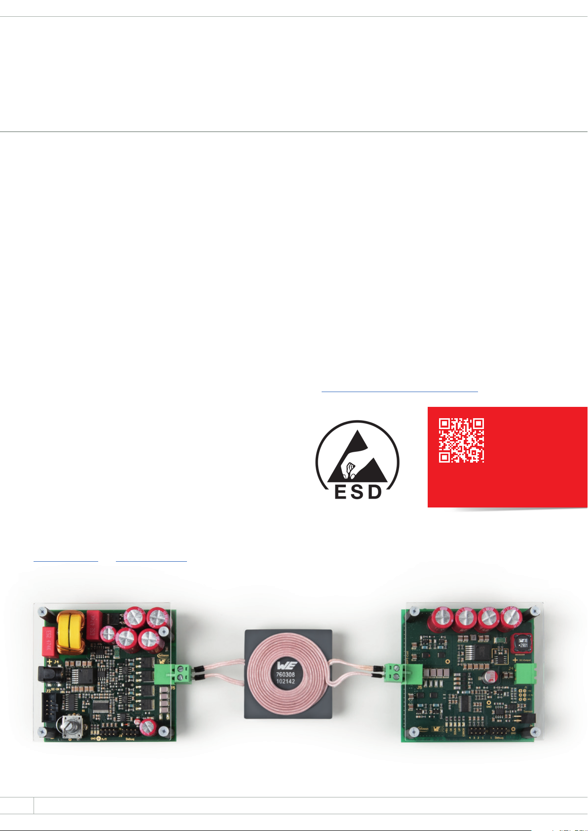
Transmitter Board and Receiver Board
Abstract
Infineon and Würth Elektronik eiSos (WE) offer this wireless power
development kit (order code 760308EMP) to demonstrate the
advantages of wireless power and to give developers the opportunity to
test and integrate a wireless power solution into their application. This
manual describes the setup and basic usage of this development kit.
Please note that this development kit is intended to be operated in a
research and development environment under supervision of qualified
technicians or engineers for test and measurement purposes. This
development kit is not designed to fulfill requirements for CE compliance.
Description of Featured Products
The BSZ070N08LS5 is a logic level OptiMOS™ 5 power MOSFET for
the synchronous rectification (SR) application which has the right RDSon level for this 200 W kit in a very compact 3.3 x 3.3 mm SMD package.
The IR1161L is a high speed SR control IC. The space saving SOT-23
package improves efficiency up to 2% over conventional secondary side
diode rectification. Its minimum on time feature is adjustable to pair with
a variety of Infineon MOSFET selections. The XMC1302, an ARM®
Cortex®-M0 up to 48 MHz, is the number one choice for your high
performance, smart and safe wireless charging application. The
760308102142 Wireless Power Transfer Coil has a high Q-factor for a
high power transfer efficiency. The 171032401 step-down converter is
easy to use, small-sized and suited for a wide range of applications. The
860160578032 are long-life electrolytic capacitors with a low ESR. For
further details, please also consult the relevant product datasheets at
www.infineon.com and www.we-online.com.
Key Specification
Mains power input voltage ....................................... 100 – 240 V
Regulated input voltage ....................................................... 24 V
Maximum transmitted power ................................................200 W
Output voltage ...............................................................19 – 20 V
Features
Plug & Play Wireless Power Development Kit
Wireless power transfer system up to 200 W
Complete solution consisting of TX and RX
Flexible and modular approach for fast integration of wireless
power in your product design
Data transfer between receiver and transmitter board
Manual and automatic output voltage control
IoT sensor I²C interface
Visit www.we-online.com/wirelesspower/200WKit for details
More information:
www.we-online.com/wirelesspower/200WKit
AC
DC
Figure 1: Wireless power transfer system with transmitter board, coils and receiver board.
www.we-online.com2
Page 3

Table of Contents
At a glance ..................................................................................................................................... 2
Abstract .................................................................................................................................... 2
Description of Featured Products ................................................................................................ 2
Key Specification ....................................................................................................................... 2
Features ................................................................................................................................... 2
1. Introduction ............................................................................................................................. 4
2. Hardware Description .............................................................................................................. 4
2.1 Block diagram ..................................................................................................................... 4
2.2 Key components................................................................................................................... 5
2.3 Design advice ...................................................................................................................... 5
2.4 Schematic, Gerber Files, Bill of Materials and Firmware .......................................................... 5
3. Development kit setup and operating hints ........................................................................... 5
3.1 Warnings ............................................................................................................................. 5
3.2 Instructions for safe use ........................................................................................................ 6
3.3 Power supply ....................................................................................................................... 6
4. Transmitter Board .................................................................................................................... 7
5. Receiver Board ......................................................................................................................... 7
6. Step by step installation guide for 200 W development kit ................................................... 8
7. Customer Support .................................................................................................................... 9
3
Page 4

1. Introduction
2. Hardware Description
This manual is valid for development kit version 1.0. It provides
guidelines to quickly setup the hardware for fast and easy evaluation
of the wireless charging system and the featured key components. For
further details and updates about the used parts, please consult
the relevant product datasheets and general information at
www.we-online.com/wirelesspower/200WKit, also for downloading
the latest version of this document and additional useful information
such as application notes, Gerber files, schematics, bill of materials,
firmware etc.
2.1 Block diagram
The development kit consists of the following components:
Transmitter board Demonstration of charging pad function using
MCU, discrete full bridge and TX coil
Receiver board Demonstration of wireless power receiver
inside a mobile device using synchronous
rectification and RX coil
Power supply Wide input range mains power supply with
different adapters for international use
A block diagram of the development kit is depicted in figure 2. The
transmitter design corresponds to a proprietary wireless power transfer
design using an XMC1302-T038X0064 to control the wireless power
transfer. The necessary 24 VDC input voltage is provided with the included
mains adapters.
The transmitter board contains the EMI-filter, reverse voltage protection,
full bridge, resonant tank and the control circuit. The power transfer is
fully digitally controlled by an XMC1302 series microcontroller. The
control signals for the full bridge are generated by the MCU and can be
controlled in automatic mode or manual mode. In manual mode the
switching frequency can be changed with the encoder. This can be used
to change the output voltage or for optimizing the efficiency.
TRANSMITTER
24 V
DC
Figure 2: Development kit block diagram
www.we-online.com4
EMV
filter
MagI³C
Step-Down
171032401
Reverse
polarity
protection
MCU
XMC1302-T038X0064
Data Receiver /
Comm
Overvoltage
protection
Full-
bridge
POWER 200 W
2 x 760308102142
DATA COMMUNICATION
RECEIVER
Rectification
(full synchronous)
MCU
XMC1302-T038X0064
Data Transmitter /
Comm
IoT I²C
Load
MagI³C
Step-Down
171032401
Sensor
Page 5

The receiver board integrates all necessary functions to act as a wireless
power receiver such as full synchronous rectification, modulator and a
WE MagI³C Power Module.
The
modulator is used for data transfer. It is controlled by the MCU to
send data from receiver side to transmitter side.The receiver is
equipped with an I²C interface that can be used to interface to
sensors. The sensor interface has its own adjustable power supply.
2.4 Schematic, Gerber Files, Bill of Materials and Firmware
Please visit www.we-online.com/wirelesspower/200WKit for downloading the latest production data consisting of the schematics, assembly
data, Gerber files, bill of materials (BOMs) and firmware files for all
boards of this development kit.
For firmware development and debugging the external tool XMC Link from
Infineon is required. More details can be found on www.infineon.com.
2.2 Key components
The purpose of the development kit is the evaluation of the key
Please note that there will be no support for the firmware since it is only
a basic functionality software which is meant for demo purposes only.
components used to realize the wireless power system. Table 1 gives an
overview of the different ICs and coils. For more detailed information
about these devices please refer to the individual web pages and
datasheets.
Manufacturer Product Family Part Number Used in
Infineon OptiMOS™ 5 Transistor BSZ070N08LS5 RX board
Infineon Synchronous Rectifier Controller IR1161L RX board
®
Infineon ARM
Würth Elektronik eiSos Wireless Power Coil 760308102142 TX and RX board
Würth Elektronik eiSos MagI³C Power Module 171032401 TX and RX board
Würth Elektronik eiSos
Table 1: Key components used in the development kit
2.3 Design advice
The switching frequency has to be higher than the resonant
frequency of the resonant tank, otherwise the output voltage can
reach a very high level.
The voltage in the resonant tank can be high. For this purpose
the voltage rating of the resonant tank capacitors have to be
considered.
Please keep in mind that when changing the output voltage the
efficiency will drop. As a consequence the temperature on some
parts will rise.
Cortex®-M0 Microcontroller XMC1302-T038X0064 AB TX and RX board
WCAP-ATLL Aluminum
Electrolytic Capacitor
860160578032 RX board
3. Development kit setup
and operating hints
3.1 Warnings
This development kit must only be operated by trained
professionals.
This development kit should be operated in a well ventilated
environment and, if used inside a case, the case should not
be covered.
This development kit should be placed on a stable, flat,
non-conductive surface in use and should not be contacted
by conductive items.
All peripherals used with the development kit should comply with
relevant standards for the country of use and be marked accordingly
to ensure that safety and performance requirements are met.
5
Page 6

All cables or connectors used must offer adequate insulation and
operation in order that the requirements of the relevant performance
and safety are met.
The connection of incompatible devices to the development kit can
cause serious damage to the unit.
Do not short any outputs to each other, to the supply or to GND
Do no operate the development kit outside its specified ratings
Take care to monitor the PCB and IC temperatures in particular
when operating with high power loads and do not exceed the
absolute maximum ratings of all components
WARNING
The AC voltage in the resonant tank may reach voltage up
to 250 Vpp under certain conditions. Therefore, it is
covered by acryl glass to ensure human safety.
Nevertheless take care not to touch the PCB by bare hand
and use the required level of isolation when probing test
points on the PCB.
3.2 Instructions for safe use
Do not expose the development kit to water, moisture or place on a
conductive surface whilst in operation
Take care whilst handling to avoid mechanical or electrical damage
to the printed circuit board and components
Avoid handling the printed circuit board while it is powered. Only
handle by the edges to minimize the risk of electrostatic discharge
damage
3.3 Power supply
Apply one of the included mains plugs (North America / Japan, Great
Britain, Central Europe) to the power supply connector and connect the
AC plug to mains. Connect the DC plug of the mains adapter to J4 of the
transmitter board. In case another power supply is used please make
sure to comply with the electrical characteristics as the provided mains
adapter (see table 2). Take care not to reverse polarize the applied
voltage.
Parameter Specification
Input voltage 100 – 240 V
Output voltage 24 V
Output Current rating 6.25 A
Table 2: Mains adapter specification
, 50/60 Hz, 2.5 A
AC
DC
MAX
Figure 3: Included power supply with 3 different mains adapter plugs
www.we-online.com6
Page 7

4. Transmitter board
5. Receiver board
Parameter Specification
Input voltage 24 V
Input current Max. 10 A
Table 3: Transmitter module specification
Parameter Specification
DC
Output voltage Max. 24 V
Output current Max. 10 A
Table 4: Receiver module specification
DC
For data communication
Controller is working
Transmitter is on
Figure 4: Transmitter board with status LEDs
Error indication: overvoltage,
overcurrent, overtemperature
On the transmitter board the error indication (red LED on) shows a fault
condition and the energy transfer stops.
Error indication: overvoltage,
overcurrent, overtemperature
Output voltage is increasing
Output voltage is decreasing
Controller OK
+ 5V OK
Figure 5: Receiver board with status LEDs
On the receiver board the error indication (red LED on) warns of a fault
condition, but the energy transfer continues.
7
Page 8

6. Step by step installation guide
for 200 W development kit
Step 1: Install software tools
Install DAVE™
DAVE™ is a free and powerful Eclipse-based development platform for
XMC™ software development.
DAVE™ includes GCC compiler from GNU, DAVE™ code engine for
automatic code generation and GDB debugger from GNU. DAVE™ offers
pre-defined and tested SW components -DAVE™ APPs- and XMC™
Lib-Low Level Drivers (LLDs) – that accelerate the application software
creation.
To install DAVE™ follow these steps:
Download and execute the latest version of DAVE™ installation file
from www.Infineon.com/DAVE
Follow the installation guidelines that are included in the download
package
Step 2: Power up setup
Make sure a load is connected to J4 on the receiver board and is
adjusted to 1 A before switching on the power supply unit. Connect the
transmitter coil to J5 on the transmitter board and the receiver coil to J5
on the receiver board (see figure 6).
Additionally a display board can be connected to the RS232 interface
(J2) of the transmitter board and a sensor with I²C interface to J6 of the
receiver board.
Step 3: Automatic and manual operation mode
By placing the jumper on position A/M on J1 (see figure 7) the transmitter
is set to manual mode. In this mode the switching frequency can be
adjusted between 100 kHz to 205 kHz referring to a coil distance of 6
mm. This function can be used to optimize the system performance or to
test different wireless power coils. When the jumper is removed the
switching frequency is set automatically to adjust output voltage to
19 – 20 V. This jumper is removed by default.
Power
Supply
RS232
Interface
Note:
Both transmitter and receiver boards are pre-flashed with the firmware.
Please visit our webpage www.we-online.com/wirelesspower/200WKit
to download the latest firmware version.
TRANSMITTER RECEIVER
J4
J5 J5
J2
J4
Load
SensorJ6
Figure 6: Block diagram for initial setup
www.we-online.com8
Page 9

S1
A/M
Jumper position for manual mode
Figure 7: Jumper setting for manual or automatic mode
Step 4: Apply power
When the setup is finished, input power can applied. The DC-OK LED on
the transmitter is on. Now the system is in standby mode. To start/stop
the wireless power transfer press S1 (see figure 7).
7. Customer Support
If any further technical supports required when operating with the
development kit please contact Würth Elektronik eiSos with your questions.
wirelesspower@we-online.com
9
Page 10

Additional Terms, warnings, restrictions and disclaimers of the Infineon and
Würth Elektronik eiSos Wireless Power Development Kit (later defined as
DEVELOPMENT KIT)
Infineon and Würth Elektronik eiSos (later defined as WE) provide the enclosed
DEVELOPMENT KIT under the following conditions:
The user has to bear all responsibility and liability for the proper and safe handling with
regard to this DEVELOPMENT KIT. The user shall indemnify Infineon and WE from all claims
arising from the handling or utilization of the DEVELOPMENT KIT. In the case this
DEVELOPMENT KIT does not comply with the specifications indicated in the Manual, the
DEVELOPMENT KIT may be returned within 30 days from the date of delivery for a full
reimbursement of the purchase price.
THE FOREGOING LIMITED WARRANTY IS THE EXCLUSIVE WARRANTY MADE BY INFINEON
AND WE TO THE USER AND IS IN LIEU OF ALL OTHER WARRANTIES, EXPRESSED, IMPLIED,
OR STATUTORY, INCLUDING ANY WARRANTY OF MERCHANTABILITY OR FITNESS FOR ANY
PARTICULAR PURPOSE. EXCEPT TO THE EXTENT OF THE INDEMNITY SET FORTH ABOVE,
NEITHER PARTY SHALL BE LIABLE TO THE OTHER FOR ANY INDIRECT, SPECIAL,
INCIDENTAL OR CONSEQUENTIAL DAMAGES.
Please read the Manual carefully prior to handling the DEVELOPMENT KIT.
This Manual contains essential safety information regarding temperatures
and voltages.
No license is granted under any patent right or other intellectual property rights of Infineon
or WE covering or relating to any machine, process and procedure, or combination in
which such the DEVELOPMENT KIT or services might be or are used. Our arrangement
with the user is not exclusive as Infineon and WE are currently working with a large number
of customers for DEVELOPMENT KITs. Infineon and WE bear no liability for applications
assistance, customer product design, software performance, or infringement of patents or
services described in the Manual.
Code of federal regulations
As noted in the DEVELOPMENT KIT Manual, this DEVELOPMENT KIT and/or accompanying
hardware may or may not be subject to and compliant with the Code of Federal Regulations,
Title 47, Part 15.
For DEVELOPMENT KITs annotated to comply with the Code of Federal Regulations, Title
47, Part 15. Operation is subject to the following two conditions: (1) This DEVELOPMENT
KIT may not cause harmful interference, and (2) this DEVELOPMENT KIT must accept any
interference received, including interference that may cause undesired operation. Changes
or modifications not expressly approved by the party responsible for compliance could void
the user‘s authority to operate the equipment. This DEVELOPMENT KIT as a Class A digital
apparatus complies with Canadian ICES-003. Changes or modifications not expressly
approved by the party responsible for compliance could void the users’ authority to operate
the equipment. For DEVELOPMENT KITs annotated as not subject to or compliant with the
Code of Federal Regulations, Title 47, Part 15. This DEVELOPMENT KIT is intended for use
for ENGINEERING DEVELOPMENT, DEMONSTRATION, OR EVALUATION PURPOSES ONLY
and is not considered by Infineon and WE to be a finished end product fit for general
consumer use. It generates, uses, and can radiate radio frequency energy and has not
been tested for compliance with the limits of computing devices pursuant to the Code of
Federal Regulations, Title 47, Part 15, which are designed to provide reasonable protection
against radio frequency interference. Operation of the equipment may cause interference
with radio communications, in which case the user at its own expense will be required to
take whatever measures may be required to correct this interference.
For Feasibility Evaluation Only, in Laboratory/Development Environments.
The DEVELOPMENT KIT is not a complete product. It is intended exclusively for preliminary
feasibility evaluation in laboratory/development environments by technically qualified
electronics experts. Those experts mandatory have to be familiar with the dangers and
application risks in connection with handling electrical mechanical components, systems
and subsystems. It should not be used as an end product or as a part of an end product.
Your Sole Responsibility and Risk. You acknowledge, represent and agree that:
a) You have unique awareness of the Federal, State and local regulatory requirements
(including but not limited to Food and Drug Administration regulations, if applicable)
which affects your products and which refers to your use (and/or the use of your
employees, affiliates, contractors or designees) of the DEVELOPMENT KIT for evaluation,
testing and other purposes.
b) You are unlimited and exclusive responsible for the safety of your DEVELOPMENT KIT
and for the compliance with all relevant laws and other applicable regulatory
requirements. Further you have to assure the safety of any activities to be conducted by
you and/or your employees, affiliates, contractors or designees, using the DEVELOPMENT
KIT. You are also responsible to ensure that any interfaces (electronic and/or mechanical)
between the DEVELOPMENT KIT and any human body are designed with suitable
isolation and means to safely limit the accessible leakage currents to minimize the risk
of electrical shock hazard.
c) Since the DEVELOPMENT KIT is not a completed product, it may not meet all applicable
regulatory and safety compliance standards (such as UL, CSA, VDE, CE, RoHS and WEEE)
which may normally be associated with similar completed products. You assume full
responsibility to determine and/or assure compliance with any such standards and related
certifications as may be applicable. You have to use reasonable safeguards to ensure that
your use of the DEVELOPMENT KIT will not result in any property damage, injury or death,
even if the DEVELOPMENT KIT should fail to perform as specified or expected.
Certain Instructions. It is important to handle this DEVELOPMENT KIT within Infineons’s
and WE‘s recommended specifications and environmental considerations as described in
the Manual. Surpassing the specified DEVELOPMENT KIT classifications (including but not
limited to input and output voltage, current, power, and environmental ranges) may cause
property damage, personal injury or death. If there are questions concerning these
classifications please contact a WE external sales representative before connecting
interface electronics including input power and intended loads. Any loads applied beyond
the specified output range may result in unintended and/or inexact operation and/or
possible lasting damage to the DEVELOPMENT KIT and/or interface electronics. Please
consult the DEVELOPMENT KIT Manual prior to connecting any load to the DEVELOPMENT
KIT output. If there is uncertainty regarding the load specification, please contact an
Infineon or WE external sales representative. During normal operation, some circuit
components may have case temperatures greater than 60°C as long as the input and
output are maintained at a normal ambient operating temperature. These components
include but are not limited to linear regulators, switching transistors, pass transistors, and
current sense resistors which can be identified by using the DEVELOPMENT KIT schematic
published in the DEVELOPMENT KIT Manual. Please be aware that the devices of the
DEVELOPMENT KIT may be very warm in case of placing the measurement test setup
close to the DEVELOPMENT KIT during normal procedure. Please ensure that only qualified
personnel educated in electronic measurement and diagnostics usually found in
development environments should use these DEVELOPMENT KITs.
Agreement to Defend, Indemnify and Hold Harmless. You agree to defend, indemnify
and hold Infineon, WE, its licensors and their representatives harmless from and against
any and all claims, damages, losses, expenses, costs and liabilities (collectively, „Claims“)
arising out of or in connection with any use of the DEVELOPMENT KIT that is not in
accordance with the terms of the agreement. This obligation shall apply whether Claims
arise under law of tort or contract or any other legal theory, and even if the DEVELOPMENT
KIT fails to perform as specified or expected.
More information or support on
www.we-online.com/wirelesspower/200WKit
wirelesspower@we-online.com
www.we-online.com
Safety-Critical or Life-Critical Applications. If you intend to evaluate the components
for possible use in safety critical applications (such as life support) where a failure of the
Infineon or WE product would reasonably be expected to cause severe personal injury or
death, such as devices which are classified as FDA Class Ill or similar classification, you
have to specifically notify Infineon or WE of such intent and enter into a separate Assurance
and Indemnity Agreement.
DIENECKARPRINZEN 760308EMPMA.1218
 Loading...