


VM1548C
TTL I/O MODULE
USER’S MANUAL
P/N: 82-0045-000
Released July 31, 2007
VXI Technology, Inc.
2031 Main Street
Irvine, CA 92614-6509
(949) 955-1894
bus

2

www.vxitech.com
TABLE OF CONTENTS
INTRODUCTION
Certification..........................................................................................................................................................6
Warranty ...............................................................................................................................................................6
Limitation of Warranty.........................................................................................................................................6
Restricted Rights Legend......................................................................................................................................6
Declaration of Conformity....................................................................................................................................7
Terms and Symbols .............................................................................................................................................. 8
Warnings ..............................................................................................................................................................8
SECTION 1..................................................................................................................................................................11
INTRODUCTION .......................................................................................................................................................11
Introduction ........................................................................................................................................................11
Features...............................................................................................................................................................12
Description .........................................................................................................................................................13
Programming and Data Access...........................................................................................................................13
VM1548 Specifications ......................................................................................................................................15
SECTION 2..................................................................................................................................................................17
PREPARATION FOR USE...........................................................................................................................................17
Installation .......................................................................................................................................................... 17
Calculating System Power and Cooling Requirements ......................................................................................17
Setting the Chassis Backplane Jumpers..............................................................................................................17
Setting the Logical Address................................................................................................................................18
Front Panel Interface Wiring .............................................................................................................................. 19
SECTION 3..................................................................................................................................................................20
PROGRAMMING....................................................................................................................................................... 20
Introduction ........................................................................................................................................................20
Notation ..............................................................................................................................................................22
EXAMPLES OF SCPI COMMANDS ............................................................................................................................23
TTLTRIG Circuit ...............................................................................................................................................23
Interrupt Circuit ..................................................................................................................................................24
Output Register Circuit.......................................................................................................................................25
Input Register Circuit .........................................................................................................................................26
Bi-directional Clock Circuit ...............................................................................................................................27
APPLICATION EXAMPLES ........................................................................................................................................28
Write Mode.........................................................................................................................................................28
Read Mode..........................................................................................................................................................30
Write/Read Mode ...............................................................................................................................................33
REGISTER ACCESS EXAMPLES ................................................................................................................................37
VXIPLUG&PLAY EXAMPLES ...................................................................................................................................39
SECTION 4..................................................................................................................................................................45
COMMAND DICTIONARY......................................................................................................................................... 45
Introduction ........................................................................................................................................................45
Alphabetical Command Listing..........................................................................................................................45
Terminology ....................................................................................................................................................... 46
Command Dictionary..........................................................................................................................................50
IEEE 488.2 COMMON COMMANDS .........................................................................................................................51
*CLS................................................................................................................................................................... 51
*ESE...................................................................................................................................................................52
*ESR?.................................................................................................................................................................53
*IDN? ................................................................................................................................................................. 54
VM1548C Preface 3

VXI Technology, Inc.
*OPC ..................................................................................................................................................................55
*RST................................................................................................................................................................... 56
*STB?.................................................................................................................................................................57
*TRG ..................................................................................................................................................................58
*TST...................................................................................................................................................................59
*WAI ..................................................................................................................................................................60
INSTRUMENT SPECIFIC SCPI COMMANDS...............................................................................................................61
FORMat..............................................................................................................................................................61
INPut:REGister:POLarity................................................................................................................................... 62
INPut:REGister:SOURce ...................................................................................................................................63
INPut:TTLTrig ...................................................................................................................................................64
INPut:TTLTrig:STATE......................................................................................................................................65
OUTPut:CLOCk:ENABle ..................................................................................................................................66
OUTPut:CLOCk:POLarity.................................................................................................................................67
OUTPut:CLOCk:SOURce..................................................................................................................................68
OUTPut:REGister:POLarity............................................................................................................................... 69
OUTPut:REGister:SOURce ...............................................................................................................................70
OUTPut:TTLTrig ...............................................................................................................................................71
OUTPut:TTLTrig:POLarity ...............................................................................................................................72
OUTPut:TTLTrig:SOURce ................................................................................................................................73
OUTPut:TTLTrig:STATE..................................................................................................................................74
READ? ...............................................................................................................................................................75
READ? CLOCks ................................................................................................................................................76
READ? CONTrol ...............................................................................................................................................77
READ? ISENse ..................................................................................................................................................78
RESet:ISENse.....................................................................................................................................................79
SOURce:DATA.................................................................................................................................................. 80
SOURce:DATA:ENABle...................................................................................................................................81
SOURce:DATA:POLarity..................................................................................................................................82
STATus:INTerrupt:ENABle ..............................................................................................................................83
STATus:INTerrupt:NTRansition........................................................................................................................84
STATus:INTerrupt:PTRansition ........................................................................................................................85
TRIGger:SEQuence:IMMediate......................................................................................................................... 86
SCPI REQUIRED COMMANDS..................................................................................................................................87
STATus:OPERation? .........................................................................................................................................87
STATus:OPERation:CONDition?......................................................................................................................88
STATus:OPERation:ENABle.............................................................................................................................89
STATus:PRESet .................................................................................................................................................90
STATus:QUEStionable:CONDition?................................................................................................................. 91
STATus:QUEStionable:ENABle .......................................................................................................................92
STATus:QUEStionable:EVENt?........................................................................................................................93
SYSTem:ERRor? ...............................................................................................................................................94
SYSTem:VERSion? ...........................................................................................................................................95
SECTION 5..................................................................................................................................................................97
THEORY OF OPERATION.......................................................................................................................................... 97
Introduction ........................................................................................................................................................97
VXI INTERFACE......................................................................................................................................................98
Device Transfers (Write Mode).......................................................................................................................... 98
Direction .............................................................................................................................................................98
Clock Enable ......................................................................................................................................................98
Data Load ...........................................................................................................................................................99
Device Triggering (TTL Input Trigger) ...........................................................................................................100
Trigger Decode.................................................................................................................................................100
Trigger Select ...................................................................................................................................................100
Device Transfers (Read Mode).........................................................................................................................102
Direction ...........................................................................................................................................................102
4 VM1548C Preface

www.vxitech.com
Clock Enable ....................................................................................................................................................102
Latch Data ........................................................................................................................................................103
Read Data .........................................................................................................................................................104
INDEX.......................................................................................................................................................................105
VM1548C Preface 5

VXI Technology, Inc.
CERTIFICATION
VXI Technology, Inc. (VTI) certifies that this product met its published specifications at the time of shipment from
the factory. VTI further certifies that its calibration measurements are traceable to the United States National
Institute of Standards and Technology (formerly National Bureau of Standards), to the extent allowed by that
organization’s calibration facility, and to the calibration facilities of other International Standards Organization
members.
WARRANTY
The product referred to herein is warranted against defects in material and workmanship for a period of three years
from the receipt date of the product at customer’s facility. The sole and exclusive remedy for breach of any warranty
concerning these goods shall be repair or replacement of defective parts, or a refund of the purchase price, to be
determined at the option of VTI.
For warranty service or repair, this product must be returned to a VXI Technology authorized service center. The
product shall be shipped prepaid to VTI and VTI shall prepay all returns of the product to the buyer. However, the
buyer shall pay all shipping charges, duties, and taxes for products returned to VTI from another country.
VTI warrants that its software and firmware designated by VTI for use with a product will execute its programming
when properly installed on that product. VTI does not however warrant that the operation of the product, or
software, or firmware will be uninterrupted or error free.
LIMITATION OF WARRANTY
The warranty shall not apply to defects resulting from improper or inadequate maintenance by the buyer, buyersupplied products or interfacing, unauthorized modification or misuse, operation outside the environmental
specifications for the product, or improper site preparation or maintenance.
VXI Technology, Inc. shall not be liable for injury to property other than the goods themselves. Other than the
limited warranty stated above, VXI Technology, Inc. makes no other warranties, express or implied, with respect to
the quality of product beyond the description of the goods on the face of the contract. VTI specifically disclaims the
implied warranties of merchantability and fitness for a particular purpose.
RESTRICTED RIGHTS LEGEND
Use, duplication, or disclosure by the Government is subject to restrictions as set forth in subdivision (b)(3)(ii) of
the Rights in Technical Data and Computer Software clause in DFARS 252.227-7013.
VXI Technology, Inc.
2031 Main Street
Irvine, CA 92614-6509 U.S.A.
6 VM1548C Preface

www.vxitech.com
D ECLARATION OF C ONFORMITY
Declaration of Conformity According to ISO/IEC Guide 22 and EN 45014
ANUFACTURER’S NAME VXI Technology, Inc.
M
ANUFACTURER’S ADDRESS 2031 Main Street
M
Irvine, California 92614-6509
RODUCT NAME TTL I/O Module
P
ODEL NUMBER(S) VM1548C
M
RODUCT OPTIONS All
P
RODUCT CONFIGURATIONS All
P
VXI Technology, Inc. declares that the aforementioned product conforms to the requirements of
the Low Voltage Directive 73/23/EEC and the EMC Directive 89/366/EEC (inclusive 93/68/EEC)
and carries the “CE” mark accordingly. The product has been designed and manufactured
according to the following specifications:
AFETY EN61010 (2001)
S
EMC EN61326 (1997 w/A1:98) Class A
CISPR 22 (1997) Class A
VCCI (April 2000) Class A
ICES-003 Class A (ANSI C63.4 1992)
AS/NZS 3548 (w/A1 & A2:97) Class A
FCC Part 15 Subpart B Class A
EN 61010-1:2001
The product was installed into a C-size VXI mainframe chassis and tested in a typical configuration.
I hereby declare that the aforementioned product has been designed to be in compliance with the relevant sections
of the specifications listed above as well as complying with all essential requirements of the Low Voltage Directive.
July 2007
VM1548C Preface 7
Steve Mauga, QA Manager
Review the following safety precautions to avoid bodily injury and/or damage to the product.
These precautions must be observed during all phases of operation or service of this product.
Failure to comply with these precautions, or with specific warnings elsewhere in this manual,
violates safety standards of design, manufacture, and intended use of the product.
Service should only be performed by qualified personnel.
TERMS AND SYMBOLS
These terms may appear in this manual:
WARNING
CAUTION
These symbols may appear on the product:
VXI Technology, Inc.
GENERAL SAFETY INSTRUCTIONS
Indicates that a procedure or condition may cause bodily injury or death.
Indicates that a procedure or condition could possibly cause damage to
equipment or loss of data.
ATTENTION - Important safety instructions
WARNINGS
Frame or chassis ground
Indicates that the product was manufactured after August 13, 2005. This mark is
placed in accordance with EN 50419, Marking of electrical and electronic
equipment in accordance with Article 11(2) of Directive 2002/96/EC (WEEE).
End-of-life product can be returned to VTI by obtaining an RMA number. Fees
for take-back and recycling will apply if not prohibited by national law.
Follow these precautions to avoid injury or damage to the product:
Use Proper Power Cord
Use Proper Power Source
Use Proper Fuse
To avoid hazard, only use the power cord specified for this product.
To avoid electrical overload, electric shock, or fire hazard, do not
use a power source that applies other than the specified voltage.
To avoid fire hazard, only use the type and rating fuse specified for
this product.
8 VM1548C Preface

www.vxitech.com
WARNINGS (CONT.)
Avoid Electric Shock
Ground the Product
Operating Conditions
Improper Use
To avoid electric shock or fire hazard, do not operate this product
with the covers removed. Do not connect or disconnect any cable,
probes, test leads, etc. while they are connected to a voltage source.
Remove all power and unplug unit before performing any service.
Service should only be performed by qualified personnel.
This product is grounded through the grounding conductor of the
power cord. To avoid electric shock, the grounding conductor must
be connected to earth ground.
To avoid injury, electric shock or fire hazard:
- Do not operate in wet or damp conditions.
- Do not operate in an explosive atmosphere.
- Operate or store only in specified temperature range.
- Provide proper clearance for product ventilation to prevent
overheating.
- DO NOT operate if any damage to this product is suspected.
Product should be inspected or serviced only by qualified
personnel.
The operator of this instrument is advised that if the equipment is
used in a manner not specified in this manual, the protection
provided by the equipment may be impaired.
Conformity is checked by inspection.
VM1548C Preface 9

VXI Technology, Inc.
SUPPORT RESOURCES
Support resources for this product are available on the Internet and at VXI Technology customer
support centers.
VXI Technology
World Headquarters
VXI Technology, Inc.
2031 Main Street
Irvine, CA 92614-6509
Phone: (949) 955-1894
Fax: (949) 955-3041
VXI Technology
Cleveland Instrument Division
5425 Warner Road
Suite 13
Valley View, OH 44125
Phone: (216) 447-8950
Fax: (216) 447-8951
VXI Technology
Lake Stevens Instrument Division
VXI Technology, Inc.
1924 - 203 Bickford
Snohomish, WA 98290
Phone: (425) 212-2285
Fax: (425) 212-2289
Technical Support
Phone: (949) 955-1894
Fax: (949) 955-3041
E-mail:
Visit
support@vxitech.com
http://www.vxitech.com for worldwide support sites and service plan information.
10 VM1548C Preface
www.vxitech.com
A
V
V
V
SECTION 1
INTRODUCTION
INTRODUCTION
The VM1548C is a high-performance I/O module that has been designed for high data throughput
and flexibility of configuration. The instrument uses the message-based word serial interface for
programming and data movement as well as allowing direct register access for very high-speed
data input and retrieval. The VM1548C command set conforms to the SCPI standard for
consistency and ease of programming.
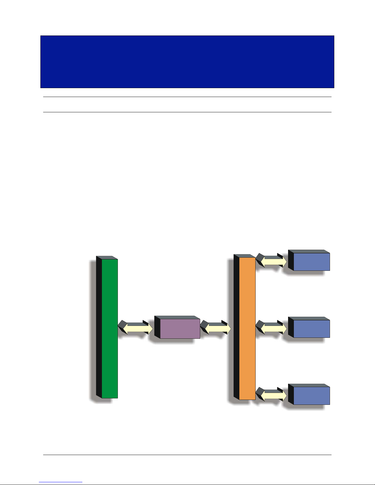
The VM1548C is a member of the VXI Technology VMIP™ (VXI Modular Instrumentation
Platform) family and is available as a 48-, 96-, or 144-channel, singlewide VXIbus instrument.
Figure 1-1 and Figure 1-2 show the 144-channel version of the VM1548C. The 96-channel
version would not have J200 and its associated LED’s and nomenclature while the 48-channel
version would eliminate J202 as well. In addition to these three standard configurations, the
VM1548C may be combined with any of the other members of the VMIP family to form a
customized and highly integrated instrument (see
system size and cost by combining the VM1548C with two other instrument functions in a single
wide, C-size VXIbus module.
Figure 1-1). This allows the user to reduce
V
X
I
B
U
S
MIP
INTERFACE
IGURE 1-1: VMIP™ PLATFORM
F
N
T
E
R
N
L
M
P
B
U
S
MIP
INSTRUMENT
MODULE #1
I
MIP
INSTRUMENT
V
I
MODULE #2
VMIP
INSTRUMENT
MODULE #3
VM1548C Introduction 11
ACC/
ERR
J200
ERR
J201
ERR
J202
bus
FAIL
FAILACC/
FAILACC/
VXI Technology, Inc.
Regardless of whether the VM1548C is configured with other VM1548C modules or
with other VMIP modules, each group of 48 channels is treated as an independent
instrument in the VXIbus chassis and as such, each group has its own FAIL/POWER
and ACCESS/ERROR indicators.
FEATURES
• 48 channels, 6 groups of 8 bits. Up to 144 channels in a single C-size card.
• Group-wise programmable, as an input or an output, through user TTL input or VXI
A16 registers.
• Group-wise programmable polarity through VXI A16 registers as an active high or
low.
• Input: 0 V to 60 V, V
IN(high)
≥ 2.0 V, V
• Output: Open collector (N-DMOS), 0 V to 60 V, up to 300 mA continuous with
over-voltage and over-current protection.
• Data throughput: 5 µs typical system speeds, 200 kilobytes (kB) per second using
D8 access, 400 kB per second using D16 access.
• Data Input/Output Clock Sources: For each group, from Front Panel clock input,
VXI TTL Trigger lines, or word serial event (command).
• Capture clock edge programmable as rising edge or falling edge.
• ASCII, Hex, Octal, and Binary data output types.
• Message or Register based data access.
• SCPI compatible.
≤ 1.5 V, input impedance ≥ 65 kΩ.
IN(low)
IGURE 1-2: FRONT PANEL LAYOUT
F
12 VM1548C Introduction

www.vxitech.com
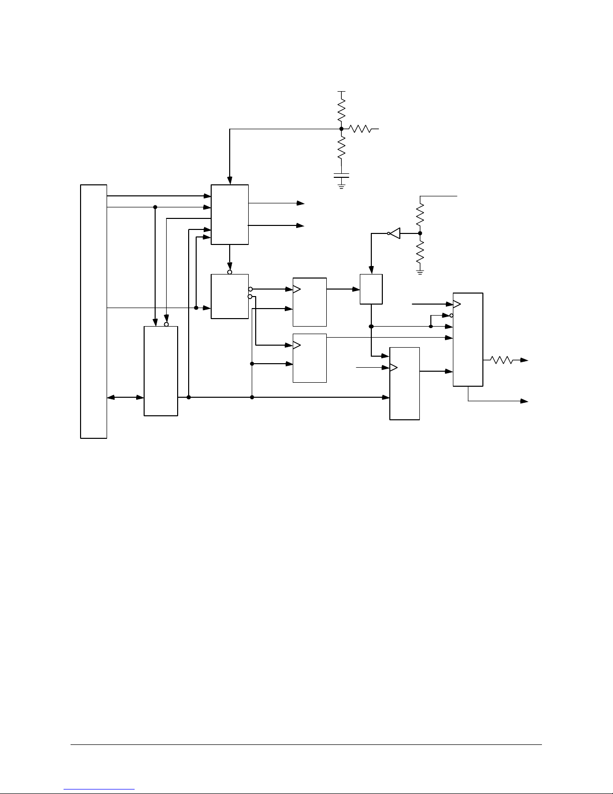
DESCRIPTION
The VM1548C Open Collector Digital I/O module is a high performance I/O module that has
been designed for high voltage, current, and data throughput. The instrument uses the messagebased word serial interface for programming and data movement as well as allowing direct
register access for very high-speed.
The VM1548C provide 48 open-collector digital I/O line that are configurable as input or output
in six groups of eight channels each. The module can drive up to 60 V with sink current of up to
300 mA per channel. Each group of 8 bits can be configured as an input or an output under
program control. The VM1548C has the flexibility to source the input and output clocks from
either the front panel (one input per group of 8 bits), the backplane TTL Trigger bus or via a word
serial command. By using the appropriate clocking sources, very large numbers of channels may
by synchronized to collect or present data to a UUT (unit under test).
Each clock input is internally pulled to a logic high level and has a RC termination network to
reduce multiple clocking due to line ringing. The RC network consists of a 120 Ω resistor in series
with a 100 pF capacitor, giving a time constant of 12 ns.
The VM1548C can be combined with any member of the VMIP family to form a customized and
highly integrated instrument.
PROGRAMMING AND DATA ACCESS
The data may be read or loaded by one of two different methods:
Word Serial Message-based Data Access: In this mode, the input or output data and all other
functions are accessed via the VXI message-based
interface. Commands are sent to set the I/O ports
as well as to initiate functions such as triggering an
update or to query a port’s input state. This data
access method is very clean from a programming
perspective, but it is also the slowest of the data
access modes.
Register-Based Data Access: This mode offers the fastest throughput. The I/O
ports are directly mapped into the VXI user
definable registers. Data access occurs in
approximately 500 ns, depending on the controller
and software used.
VM1548C Introduction
13
VXI Technology, Inc.
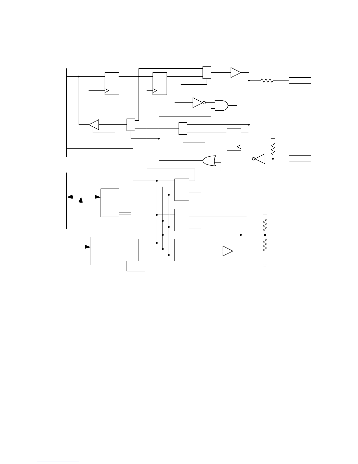
FRONT
PANEL
22
DATA I/O
WRITE
DATA
A
DQDQ
CLKOUTENA
ISENSE
B
DAMPING
RESISTOR
VMIP BUSVXI BACKPLANE
TTL TIGGER 0-7
8:1
SELECT
READ
DATA
8:1
SELECT
A
B
TTL
TRIGGER
SELECT
1:3
SELECT
TTL TRIG
OUT SEL
F
IGURE 1-3: VM1548C MODULE BLOCK DIAGRAM
A
B
3:1
MUX
3:1
MUX
3:1
MUX
CLKINENA
CLK OUT
SEL
CLK IN
SEL
CLKOUTENA
QD
OUTENA
47K
I/O*
47K
CLOCK
120
100pF
14 VM1548C Introduction

www.vxitech.com
VM1548 SPECIFICATIONS
GENERAL SPECIFICATIONS
NUMBER OF CHANNELS
VM1548C-1
VM1548C-2
VM1548C-3
DIRECTION
DATA THROUGHPUT
48, 6 groups of 8 bits
96, 12 groups of 8 bits
144, 18 groups of 8 bits
bi-directional
5 µs typical system (500 µs register cycle time)
200 kB/s using D8 access
400 kB/s using D16 access
PHYSICAL INTERFACE
N channel DMOS transistor (TPIC2601KTC) with a current protection circuit on
the output side, and a voltage divider and voltage comparator on the input side
CHANNEL INPUT CHARACTERISTICS
V
V
V
Input Impedance
IN(high)
IN(low)
IN(max)
≥ 2.0 V
≤ 1.5 V
≤ 60 V
≥ 65 kΩ
CHANEL OUTPUT CHARACTERISTICS
V
OUT(max)
Current Sink (Max.)
Switch On Time
≤ 60 V
≤ 300 mA
≤ 1 µs
CLOCK AND CONTROL INPUT CHARACTERISTICS
V
V
IN(high)
IN(low)
Current In (VIN = 5.0 V)
> 2.0 V
< 0.8 V
< 10 µA
DATA INPUT CLOCK SOURCES
6 front panel
TTL trigger bus (0 - 7)
word serial command
TTL TRIGGER OUTPUT SOURCES
CLOCKED INPUT DATA SETUP
Front Panel Clock inputs (0 - 5)
≥ 2 µs
CLOCKED INPUT DATA HOLD
≥ 0
CLOCKED DATA OUTPUT SKEW
POWER REQUIREMENTS
≤ 2 µs
+5 V @ 864 mA, +12 V @ 60 mA
COOLING REQUIREMENTS
VM1548C-1
VM1548C-2
VM1548C-3
0.4 L/s
0.8 L/s
1.2 L/s
VM1548C Introduction
15

VXI Technology, Inc.
16 VM1548C Introduction

www.vxitech.com
SECTION 2
PREPARATION FOR USE
INSTALLATION
When the VM1548C is unpacked from its shipping carton, the contents should include the
following items:
(1) VM1548C VXIbus module
(1) VM1548C Open Collector Digital I/O Module User’s Manual (this manual)
All components should be immediately inspected for damage upon receipt of the unit.
Once the VM1548C is assessed to be in good condition, it may be installed into an appropriate
C-size or D-size VXIbus chassis in any slot other than slot 0. The chassis should be checked to
ensure that it is capable of providing adequate power and cooling for the VM1548C. Once the
chassis is found to be adequate, the VM1548C’s logical address and the chassis’ backplane
jumpers should be configured prior to the VM1548C’s installation.
CALCULATING SYSTEM POWER AND COOLING REQUIREMENTS
The power and cooling requirements of the VM4018 are given in the Specifications section of
Section 1 in this manual. It is imperative that the chassis provide adequate power and cooling for
this module. Referring to the chassis User’s Manual, confirm that the power budget for the system
(the chassis and all modules installed therein) is not exceeded and that the cooling system can
provide adequate airflow at the specified backpressure.
It should be noted that if the chassis cannot provide adequate power to the module, the instrument
might not perform to specification or possibly not operate at all. In addition, if adequate cooling is
not provided, the reliability of the instrument will be jeopardized and permanent damage may
occur. Damage found to have occurred due to inadequate cooling will void the warranty on the
instrument in question.
SETTING THE CHASSIS BACKPLANE JUMPERS
Please refer to the chassis User’s Manual for further details on setting the backplane jumpers.
VM1548C Preparation for Use 17
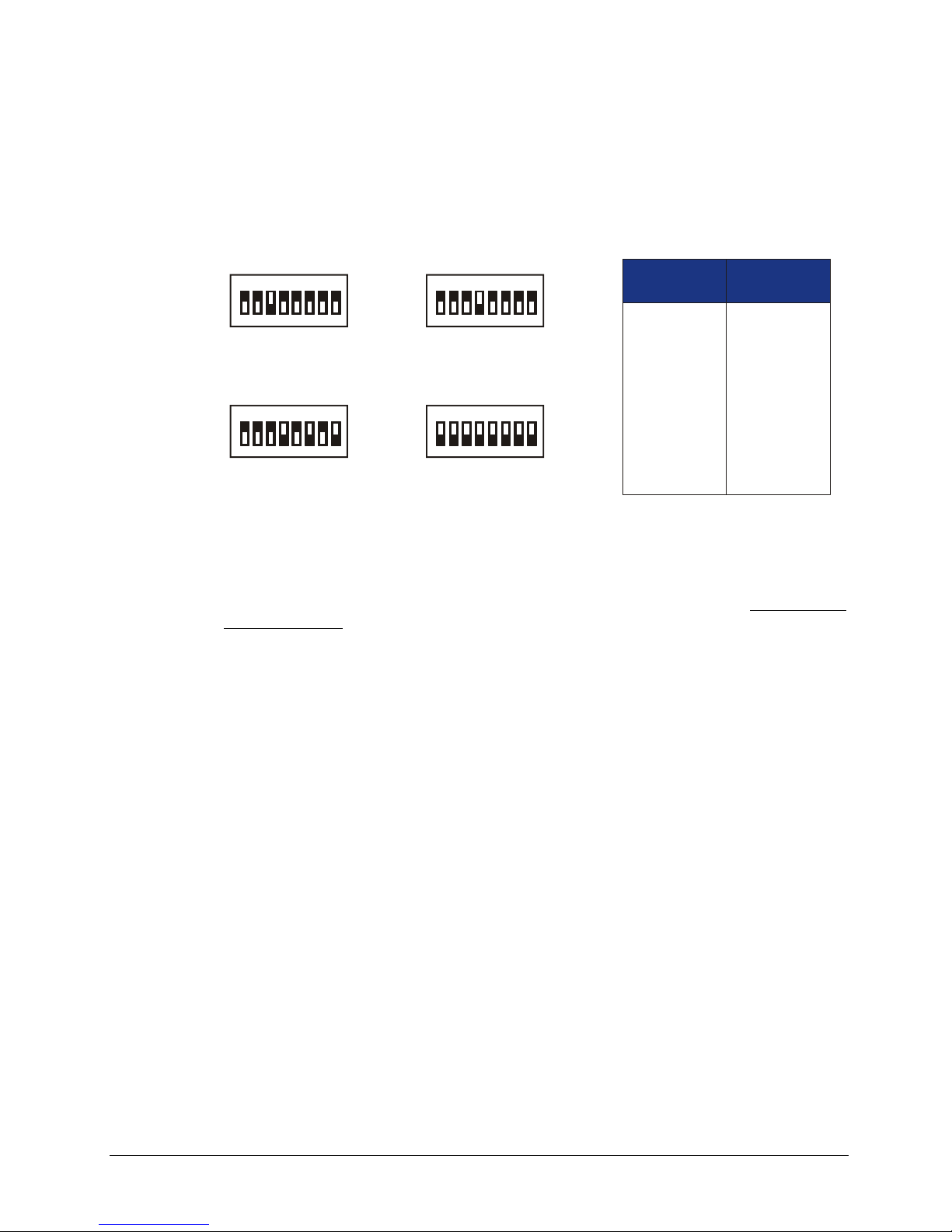
SETTING THE LOGICAL ADDRESS
The logical address of the VM1548C is set by a single 8-position DIP switch located near the
module’s backplane connectors (this is the only switch on the module). The switch is labeled with
positions 1 through 8 and with an ON position. A switch pushed toward the ON legend will signify
a logic 1; switches pushed away from the ON legend will signify a logic 0. The switch located at
position 1 is the least significant bit while the switch located at position 8 is the most significant
bit. See
Figure 2-1 for examples of setting the logical address switch.
VXI Technology, Inc.
ON ON
1ON2345678
SET TO 4
ON ON
12345678
SET TO 168
F
IGURE 2-1: LOGICAL ADDRESS SWITCH SETTING EXAMPLES
1ON2345678
SET TO 8
1
2345678
SET TO 255
(Dynamic)
Switch
Position
1
2
3
4
5
6
7
8
Switch
Value
1
2
4
8
16
32
64
128
The VMIP may contain three separate instruments and will allocate logical addresses as required
by the VXIbus specification (revisions 1.3 and 1.4). The logical address of the instrument is set on
the VMIP carrier. The VMIP logical addresses must be set to an even multiple of 4 unless dynamic
addressing is used. Switch positions 1 and 2 must always be set to the OFF position. Therefore,
only addresses of 4, 8, 12, 16, ...252 are allowed. The address switch should be set for one of these
legal addresses and the address for the second instrument (the instrument in the center position)
will automatically be set to the switch set address plus one; while the third instrument (the
instrument in the lowest position) will automatically be set to the switch set address plus two. If
dynamic address configuration is desired, the address switch should be set for a value of 255 (All
switches set to ON). Upon power-up, the slot 0 resource manager will assign the first available
logical addresses to each instrument in the VMIP module.
If dynamic address configuration is desired, the address switch should be set for a value of 255.
Upon power-up, the slot 0 resource manager will assign logical addresses to each instrument in the
VMIP module.
18 VM1548C Preparation for Use

www.vxitech.com
FRONT PANEL INTERFACE WIRING
The VM1548C’s module interface is made available on the front panel of the instrument. The
48-channel version (VM1548C-1) will have J201, which contains all signals for this instrument.
The 96-channel version (VM1548C-2) will have J201 and J202 provided, while the 144-channel
version (VM1548C-3) will have J200, J201 and J202. The wiring for each of these connectors is
identical and since each group of 48 channels is treated as a separate instrument, the module will
have three Channel 1s, three Channel 2s, three Channel 3s, etc.
The connector used in the VM1548C is a readily available 68-pin high-density type commonly
known as a 68-pin version of the SCSI 2 connector. The mating connector is an IDC (Insulation
Displacement Connector) component and is available from a variety of sources. The connector
attaches to two 34-conductor 0.050 centers ribbon cable, and the pin out has been selected to allow
for using the twisted pair type of ribbon cable. Some manufacturers also allow the use of discrete
30 gauge stranded wires.
ABLE 2-1: J200, J201 AND J202 PIN OUTS
T
PIN SIGNAL PIN SIGNAL PIN SIGNAL PIN SIGNAL
1 GND 18 DATA1.5 35 GND 52 DATA4.5
2 DATA0.0 19 DATA1.6 36 DATA3.0 53 DATA4.6
3 DATA0.1 20 DATA1.7 37 DATA3.1 54 DATA4.7
4 DATA0.2 21 I/O*1 38 DATA3.2 55 I/O*4
5 DATA0.3 22 CLK1 39 DATA3.3 56 CLK4
6 DATA0.4 23 GND 40 DATA3.4 57 GND
7 DATA0.5 24 DATA2.0 41 DATA3.5 58 DATA5.0
8 DATA0.6 25 DATA2.1 42 DATA3.6 59 DATA5.1
9 DATA0.7 26 DATA2.2 43 DATA3.7 60 DATA5.2
10 I/O*0 27 DATA2.3 44 I/O*3 61 DATA5.3
11 CLK0 28 DATA2.4 45 CLK3 62 DATA5.4
12 GND 29 DATA2.5 46 GND 63 DATA5.5
13 DATA1.0 30 DATA2.6 47 DATA4.0 64 DATA5.6
14 DATA1.1 31 DATA2.7 48 DATA4.1 65 DATA5.7
15 DATA1.2 32 I/O*2 49 DATA4.2 66 I/O*5
16 DATA1.3 33 CLK2 50 DATA4.3 67 CLK5
17 DATA1.4 34 GND 51 DATA4.4 68 GND
VM1548C Preparation for Use 19

VXI Technology, Inc.
The mating connector to J200, J201 or J202 is available from the following companies:
AMP Inc.
P/N 749111-6 Connector
P/N 749204-2 Back Shell
P/N 82208 Catalog covering this series of connectors
Circuit Assembly
P/N CA-68NDP-12GT Connector
P/N CA-68NDBS-1M Back Shell
P/N DG01 Catalog covering this series of connectors
The pin locations for J200, J201, and J202 are shown in
PIN 1 PIN 35
Figure 2-2.
PIN 34
F
IGURE 2-2: J200, J201, AND J202 PIN LOCATIONS
PIN 68
SECTION 3
PROGRAMMING
INTRODUCTION
The VM1548C is a VXIbus message-based device whose command set is compliant with the
Standard Command for Programmable Instruments (SCPI) programming language.
20 VM1548C Preparation for Use

www.vxitech.com
All module commands are sent over the VXIbus backplane to the module. Commands may be in
upper, lower, or mixed case. All numbers are sent in ASCII decimal unless otherwise noted.
The module recognizes SCPI commands. SCPI is a tree-structured language based on IEEE-STD-
488.2 Specifications. It utilizes the IEEE-STD-488.2 Standard command, and the device
dependent commands are structured to allow multiple branches off the same trunk to be used
without repeating the trunk. To use this facility, terminate each branch with a semicolon.
See the Standard Command for Programmable Instruments (SCPI) Manual, Volume 1: Syntax &
Style, Section 6, for more information.
The SCPI commands are listed in upper and lower case. Character case is used to indicate
different forms of the same command. Keywords can have both a short form and a long form
(some commands only have one form). The short form uses just the keyword characters in
uppercase. The long form uses the keyword characters in uppercase plus the keyword characters
in lowercase. Either form is acceptable. Note that there are no intermediate forms. All characters
of the short form or all characters of the long form must be used. Short forms and long forms may
be freely intermixed. The actual commands sent can be in upper case, lower case, or mixed case
(case is only used to distinguish short and long form for the user). As an example, these
commands are all correct and all have the same effect:
TRIGger:SEQuence:IMMediate
trigger:sequence:immediate
TRIGGER:SEQUENCE:IMMEDIATE
TRIG:SEQuence:IMMediate
TRIG:SEQ:IMMediate
TRIG:SEQ:IMM
trig:seq:IMM
trig:seq:imm
VM1548C Programming 21

NOTATION
VXI Technology, Inc.
The following command is not correct because it uses part of the long form of TRIGger, but not
all the characters of the long form:
trigg:seq:imm (incorrect syntax - extra "g"- only trig or trigger is correct)
All of the SCPI commands also have a query form unless otherwise noted. Query forms contain a
question mark (?). The query form allows the system to ask what the current setting of a
parameter is. The query form of the command generally replaces the parameter with a question
mark (?). Query responses do not include the command header. This means only the parameter is
returned: no part of the command or "question" is returned.
Keywords or parameters enclosed in square brackets ([ ]) are optional. If the optional part is a
keyword, the keyword can be included or left out. Omitting an optional parameter will cause its
default to be used.
Parameters are enclosed by angle brackets (< >). Braces ({ }), or curly brackets, are used to
enclose one or more parameters that may be included zero or more times. A vertical bar (|), read
as "or", is used to separate parameter alternatives.
22 VM1548C Programming

www.vxitech.com
EXAMPLES OF SCPI COMMANDS
TTLTRIG CIRCUIT
A multiplexer is used to select 1 of 8 different sources as TTLTRIG. The signal is selected using
the following SCPI command:
OUTPut:TTLTrig:SOURce <source> Where <source> refers to one of
The selected signal is called GLOBAL (TRIGOUT) and after a polarity control, it is called
TTLTRIGGER, which is presented on the VXIbus as the selected TTLTRIG0-7. The specific
TTLTRIG line is selected using the following SCPI command:
OUTPut:TTLTrig <n> Where <n> refers to one of the 8
The TTLTRIGGER is enabled or disabled using the following SCPI command:
OUTPut:TTLTrig:STATe ON Enables the Trigger
OUTPut:TTLTrig:STATe OFF Disables the Trigger
The following is an example of how to produce CLK2 as TTLTRIG4 to the backplane:
OUTPut:TTLTrig:STATe ON
OUTPut:TTLTrig:POLarity NORMal
OUTPut:TTLTrig 4
OUTPut:TTLTrig:SOURce EXTERNAL2
If CLK2 is a logic low level, then the following SCPI command would allow a logic high level on
the backplane.
OUTPut:TTLTrig:POLarity INVERT TTLTRIG 4 will not pull the line
Likewise, continuing with this example, the following command would produce a logic low level
on the backplane.
OUTPut:TTLTrig:POLarity NORMal TTLTRIG 4 will pull the line low
the EXTERNAL CLK lines (CLK0-
5), IMMEDIATE or NONE.
TTLTRIG lines.
low
VM1548C Programming 23

INTERRUPT CIRCUIT
This section deals with the interrupt circuit. The VM1548C has the capability to interrupt the slot
0 controller via the VMIP with either a high going edge or with a low going edge of the IRQ*
signal. The timing and control circuitry can select one of the six EXTERNAL clocks, GLOBAL
(TRIGOUT) or NONE as the interrupt trigger. The interrupt is selected and enabled using the
following SCPI command:
STATus:INTerrupt:ENABle <source> Where <source> is EXTERNAL0-
The following SCPI command will trigger the status interrupt on a positive edge:
STATus:INTerrupt:PTRansition ON
The following SCPI command will trigger the status interrupt on a negative edge:
STATus:INTerrupt:NTRansition ON
EXAMPLES
To use GLOBAL (TRIGOUT) out as the status interrupt trigger, the following SCPI command
would be issued:
STATus:INTerrupt:ENABle GLOBAL
To trigger the status interrupt from a negative going edge external clock source from port 3, the
following SCPI commands would be issued:
STATus:INTerrupt:ENABle EXTERNAL3
STATus:INTerrupt:NTRansition ON
To trigger the status interrupt from a negative edge going external clock source from port 1, the
following SCPI commands would be issued:
STATus:INTerrupt:ENABle EXTERNAL1
STATus:INTerrupt:NTRansition ON
VXI Technology, Inc.
5, GLOBAL or NONE
24 VM1548C Programming

www.vxitech.com
OUTPUT REGISTER CIRCUIT
This section refers to the bi-directional port when configured as an output. The SCPI command
used to configure a port as an output is:
SOURce:DATA:ENABle <port #> ON
The port is programmable to allow the data to be transparent or clocked. If the port is clocked,
there are several choices for the clock source. The method for selecting clocked mode and the
source of the clock is done with one SCPI command.
OUTPut:REGister:SOURce <port #> <source> Where <port> is 1 of 6 data
The method for selecting transparent mode is:
OUTPut:REGister:SOURce <port #> NONE Where <port> is 1 of 6 data
EXAMPLES
The following SCPI commands will clock the number 205 out of port #5 using the IMMEDIATE
pulse.
SOURce:DATA:ENABle 5 ON
OUTPut:REGister:SOURce 5 IMMEDIATE
SOURce:DATA 5 205
TRIGger:SEQuence:IMMediate This provides a rising edge clock
The following is an example of writing to a port operating in transparent mode. This method
requires no clock edge for the data to be presented on the external connector.
SOURce:DATA:ENABle 5 ON
OUTPut:REGister:SOURce 5 NONE
SOURce:DATA 5 205 205 Immediately appears on the
The following example selects the external CLK5 line to clock the data port. In this example, it is
assumed the external CLK5 signal is a steady logic low and the clock edge is produced by
toggling the clock polarity.
SOURce:DATA:ENABle 5 ON
OUTPut:REGister:SOURce 5 EXTERNAL
OUTPut:REGister:POLarity 5 NORMAL
SOURce:DATA 5 205
OUTPut:REGister:POLarity 5 INVERT This provides a rising edge clock
registers and <source> is
EXTERNAL, TTLTRIG, GLOBAL
(TRIGOUT) or IMMEDIATE
registers and NONE means this
data register is transparent
External Connector
VM1548C Programming 25

INPUT REGISTER CIRCUIT
This section refers to the bi-directional port when configured as an input. The SCPI command
used to configure a port as an input is:
SOURce:DATA:ENABle <port #> OFF
The port is programmable to allow the data to be transparent or clocked. If the port is clocked,
there are several choices for the clock source. The method for selecting clocked mode and the
source of the clock is done with one SCPI command.
INPut:REGister:SOURce <port #> <source> Where <port> is 1 of 6 data
Regardless of the port’s input mode, note that data inputs to the module do not contain pull-up or
down-biasing resistors. As such, if the user does not provide either active or passive biasing of the
data inputs, a read of the port may result in either a “1” or a “0” being read from the data inputs.
The method for selecting transparent mode is:
INPut:REGister:SOURce <port #> NONE Where <port> is 1 of 6 data
EXAMPLES
The following SCPI commands will clock the data in on port #3 using the IMMEDIATE pulse.
SOURce:DATA:ENABle 3 OFF
INPut:REGister:SOURce 3 IMMEDIATE
TRIGger:SEQuence:IMMediate This provides a rising edge clock
FORMat ASCII
READ? 3 Example of read value is 255
The following is an example of reading from a port operating in transparent mode. This method
requires no clock edge for the data to be available.
SOURce:DATA:ENABle 5 OFF
INPut:REGister:SOURce 5 NONE
FORMat BINARY
READ? 5 The data presented on the external
The following example selects the external CLK3 line to clock the data port. In this example, it is
assumed the external CLK3 signal is a steady logic low and the clock edge is produced by
toggling the clock polarity.
SOURce:DATA:ENABle 3 OFF
INPut:REGister:SOURce 3 EXTERNAL
INPut:REGister:POLarity 3 NORMAL
INPut:REGister:POLarity 3 INVERT This provides a rising edge clock
FORMat HEX
READ? 3
Example of read value is #HFF
VXI Technology, Inc.
registers and <source> is
EXTERNAL, TTLTRIG, GLOBAL
(TRIGOUT) or IMMEDIATE
registers and NONE means this
data register is transparent
Example of read value is
#B11111111
connector is what will be read
26 VM1548C Programming

www.vxitech.com
BI-DIRECTIONAL CLOCK CIRCUIT
There are six independent bi-directional clock circuits connected to the 68-pin external connector.
Each clock is associated with one of the 6 ports previously described. Therefore, <port #>
terminology is used to refer to a specific clock. When the circuit is configured as an output, the
clock signal will be sourced by the module. When the circuit is configured as an input, the clock
signal is sourced by the UUT. This clock (CLK0-5) may be used for many different purposes: a
trigger source; selections for the interrupt trigger; a port’s input clock; a port’s output clock.
The following SCPI command configures the clock line as an output:
OUTPut:CLOCk:ENABle ON
The following SCPI command configures the clock line as an input:
OUTPut:CLOCk:ENABle OFF
When the circuit is operating as an output, the clock source is selectable using the following SCPI
command.
OUTPut:CLOCk:SOURce <port #> <source> Where <source> is TTLTRIG,
The polarity of the output clock signal is controlled with the following SCPI command.
OUTPut:CLOCk:POLarity <edge> Where <edge> is NORMAL or
EXAMPLES
To drive TRIGIN out as CLK1 on the external connector, the following SCPI commands would
be issued.
OUTPut:CLOCk:ENABle 1 ON
OUTPut:CLOCk:SOURce TTLTRIG
To drive TRIGOUT out as CLK3 on the external connector, the following SCPI commands would
be issued:
OUTPut:CLOCk:ENABle 3 ON
OUTPut:CLOCk:SOURce GLOBAL
To drive IMMEDIATE out as CLK5 on the external connector, the following SCPI commands
would be issued:
OUTPut:CLOCk:ENABle 5 ON
OUTPut:CLOCk:SOURce IMMEDIATE
To select no clock, the NONE parameter is used. This will always be a logic level low.
OUTPut:CLOCk:ENABle 5 ON
OUTPut:CLOCk:SOURce NONE
IMMEDIATE, GLOBAL
(TRIGOUT) or NONE
INVERT
VM1548C Programming 27

APPLICATION EXAMPLES
This section contains examples of using SCPI command strings for programming the VM1548C
module. The code is functional and will contain a brief description and block diagram of the
operation.
WRITE MODE
In this example the VM1548C will be set up prior to receiving the UUT generated clock edge.
The VM1548C will output one (1) 16-bit binary word to the UUT from ports 0 and 1.
COMMANDS
OUTP:CLOC:ENAB 0 0 Disables port 0 clock from driving front panel
OUTP:CLOC:ENAB 1 0 Same as previous command except for port 1.
OUTP:REG:SOUR 0 EXT Selects port 0 input clock (CLK0) as method of
OUTP:REG:SOUR 1 EXT Same as previous command except for port 1.
SOUR:DATA:ENAB 0 1 Selects and enables port 0 to write data to the UUT.
STAT:INT:ENAB EXT0 Set the interrupt trigger source as the port 0 clock.
STAT:INT:PTR ON Set the interrupt trigger source to the positive edge.
SOUR:DATA 0 48 Writes “48” data to port 0 for subsequent transfer to
SOUR:DATA:ENAB 1 1 Selects and enables port 1 to write data to the UUT.
SOUR:DATA 1 15 Writes “15” data to port 1 for subsequent transfer to
Figure 3-1 and the description that follows illustrates the function of each of the commands above.
DESCRIPTION
VXI Technology, Inc.
connector and enables this line as the clock input to
port 0.
triggering.
the UUT.
the UUT.
28 VM1548C Programming
www.vxitech.com
VCC
47K
120
22
100pF
CLK from
front panel
VMIP
Bus
Control Lines
Address 0,1,2
Data Bus
Read /
Write
Data
Buffer
WRITE*
DOE*
D8-D15
Timing
and
Control
Port
Decoder
F
WRITE
CLKOUT <port>
PORTENA*
Write
Clock
Data Bus
OUTENA
PORT2*
D8-D15
PORT1*
Direction
Control
Enable
IGURE 3-1: OUTPUT BLOCK DIAGRAM
OR
WRITE
CLKOUT <port>
IN*/OUT <port>
CLKOUTENA
I/O
Word
Buffer
200K
33K
Data Bus
I/O from
front panel
Output
Data
Buffer
22
ISENSE
OUTP:CLOC:ENAB 0 0 and OUTP:CLOC:ENAB 1 0 commands inform the timing and
control circuitry that the front panel clock lines are used as inputs. This allows the UUT to furnish
the clock source when ready to receive data.
The OUTP:REG:SOUR 0 EXT and the OUTP:REG:SOUR 1 EXT commands select the
external clock input as the trigger method to output data to the UUT. When these commands are
received the VM1548C timing and control circuitry will generate the PORTENA* signal to the
port decoder. The port decoder then clocks the write clock enable latch selecting the
CLKOUTENA. The CLKOUTENA signals are applied to the I/O data and word buffers enabling
the output clock line. The SOUR:DATA:ENAB 0 1 and SOUR:DATA 0 48 command enables
port 0 for a write and latches the data into the I/O word buffer respectively.
VM1548C Programming 29

READ MODE
VXI Technology, Inc.
The VM1548C timing and control circuitry generates the PORTENA* signal to the port decoder.
This decoder in turn clocks the direction latch selecting the OUTENA. This signal is OR’ed with
the external I/O direction signal from the UUT. The result is referred to as IN*/OUT and is
applied to the I/O data and word buffers configuring them as outputs. The timing and control
circuitry will generate a write pulse latching the data from the read/write data buffer into the I/O
word buffer. Port 0 is now ready to transmit the data byte “48” to the UUT. The steps are repeated
for the SOUR:DATA:ENAB 1 1 and SOUR:DATA 1 15 commands with port 1 being enabled
and loaded with the data byte “15”.
The VM1548C is now ready to transmit the data word “1548C” to the UUT. When the CLK
signals are received from the UUT, the I/O data buffers latch the data word from the I/O word
buffer. The data on the I/O data buffer’s outputs are now available to the UUT. The
STAT:INT:ENAB EXT 0 and STAT:INT:PTR ON commands enable the interrupt to occur
when the CLK 0 signal is received and sets the polarity of this interrupt to the positive edge. The
VM1548C module sends an Interrupt Request (IRQ*) informing the slot 0 controller that the
transfer has occurred.
In this example the VM1548C will be configured to clock the UUT and read 24 bits of data, when
the TTL Trigger line 1 is activated. The TTL Trigger is assumed to be pulled by another
instrument used during this test. The UUT will output data on the rising edge of the received clock
that is generated from the VM1548C. The VM1548C will capture or read data on the falling edge
of this same clock. When the VM1548C detects a TTL Trigger 1, the front panel clock lines to the
UUT are activated. The clock is sent, the UUT transmits data on the rising edge, and the data will
be latched into the VM1548C on the falling edge. An Interrupt Request is generated informing the
slot 0 controller via the VMIP that data is ready to be read.
COMMANDS
OUTP:CLOC:ENAB 3 ON Enables port 3 clock to drive the front panel
DESCRIPTION
connector
OUTP:CLOC:ENAB 4 ON Same as previous command except for port 4
OUTP:CLOC:ENAB 5 ON Same as previous command except for port 5
SOUR:DATA:ENAB 3 OFF Selects and enables port 3 to read data from the UUT
SOUR:DATA:ENAB 4 OFF Selects and enables port 4 to read data from the UUT
SOUR:DATA:ENAB 5 OFF Selects and enables port 5 to read data from the UUT
INP:REG:POL 3 INV Selects the falling edge for clocking port 3
INP:REG:POL 4 INV Selects the falling edge for clocking port 4
INP:REG:POL 4 INV Selects the falling edge for clocking port 5
INP:REG:SOUR 3 TTLT Selects VXI bus TRIGIN as the clock source for
port 3
INP:REG:SOUR 4 TTLT Same as previous command except for port 4
INP:REG:SOUR 5 TTLT Same as previous command except for port 5
INP:TTLT:STATE ON Enables the TTL trigger selection mux
INP:TTLT 1 Selects VXI bus TTL trigger line 1 to be used as
TRIGIN
STAT:INT:ENAB Set the interrupt trigger source as the default value
STAT:INT:NTR ON Set the interrupt trigger source to the negative edge
The controller waits for the interrupt and then
proceeds
READ? 3 Data is transferred from port 3 to the VMIP bus
READ? 4 Data is transferred from port 4 to the VMIP bus
READ? 5 Data is transferred from port 5 to the VMIP bus
30 VM1548C Programming

www.vxitech.com
Below, Figure 3-2 illustrates what occurs when these commands are executed. The description
that follows illustrates the role of each command.
TRIGIN0-7
Trigger
In Mux
TRIGIN*
VCC
VMIP
Bus
Control Lines
Address 0,1,2
Data Bus
Read /
Write
Data
Buffer
WRITE*
DOE*
D8-D15
Timing
and
Control
Port
Decoder
F
IGURE 3-2: READ MODE USING TTL TRIGGER IN
IN*/OUT <port>
READ
READ <port>
CLKIN <port>
PORTENA*
PORT3*
D8-D15
Trigger
Select
TINENA*
TINSEL0,1,2
Read <port>
Read
I/O
Word
Buffer
47K
120
100pF
CLKIN <port>
IN*/OUT <port>
Data Bus
22
CLKIO <port>
to front panel
Input
Data
Buffers
(ports 3,4,5)
22
VM1548C Programming 31

VXI Technology, Inc.
The OUTP:CLOC:ENAB <port> ON command configures the front panel clock connection to
the output mode. This allows the VM1548C to drive these lines clocking the UUT. The timing
and control circuitry generates the IN*/OUT <port> signal to the I/O data and word buffers
configuring them as inputs when the SOUR:DATA:ENAB <port> 1 commands are received.
The INP:REG:SOUR <port> TTLT commands select the VXI TTL trigger in as the clock input
for the trigger method to input data from the UUT. This clock is transmitted from the front panel
connectors, clocking the data out of the UUT. When the commands are received the VM1548C
timing and control circuitry will generate the PORTENA* signal to the port decoder. The port
decoder then clocks the write clock enable latch selecting the CLKINENA. The CLKINENA
signals are applied to the I/O data and word buffers enabling the input clock line.
The INP:REG:POL <port> INV command causes the timing and control circuitry to select the
falling edge of the TTL trigger in as the CLKIN <port> for the I/O data buffers.
When INP:TTLT:STATE ON command is received, the VM1548C timing and control circuitry
generates the PORTENA* signal to the port decoder. This clocks the trigger select latch selecting
the TINENA line. The TINENA signal enables the trigger in mux. INP:TTLT 1 notifies the
timing and control circuitry to select TTL trigger 1 for the clock source. The port decoder is again
enabled to clock the trigger select latch selecting the TINSEL signals. These signals are routed to
the trigger in mux that enables TTL trigger 1 to be routed to the timing and control circuitry for
clocking the UUT and the I/O data buffers. The normal polarity of the trigger is sent to the UUT
and the inverted version is used for the I/O data buffers.
The STAT:INT:ENAB command uses the default value of NONE (ground) to generate the status
interrupt onto the VXI backplane and the STAT:INT:PTR ON command set the polarity of the
interrupt. When the TTL trigger 1 occurs, the VM1548C will send a high going pulse to clock
data out of the UUT. The falling edge of this pulse is used to latch the data into the VM1548C’s
I/O data buffers. The VM1548C sends an Interrupt Request (IRQ*) informing the slot 0 controller
via the VMIP that the transfer has occurred and that the data in the I/O data buffers is now
available. The READ? <port> command causes the timing and control circuitry to generate two
READ signals. The first READ signal is routed to the I/O word buffers thereby enabling them to
output data to the read/write data buffer and onto the VMIP bus. The second signal READ (0,2,4)
then clocks the I/O word buffer. The I/O word buffer will output one 16-bit word at a time.
Note that data inputs to the module do not contain pull-up or down-biasing resistors. If the user
does not provide active or passive biasing of the data inputs, a read of the port may result in either
a “1” or “0” being read from the data inputs.
32 VM1548C Programming

www.vxitech.com
WRITE/READ MODE
In this example, a wrap-around cable will be used to configure and transfer data from port 0,
port 1, and port 2 to port 3, port 4, and port 5. The wrap-around cable pin outs used are as defined
Table 3-1. The data to be sent is port 0 = 01, port 1 = 23, and port 2 = 45. The IRQ* signal will
in
be generated from the external clock received from port 5.
COMMANDS
INP:REG:SOUR 3 EXT Selects External clock line as the clock source for
INP:REG:POL 3 INV Selects the inverted (falling) clock edge for port 3
INP:REG:SOUR 4 EXT Selects External clock line as the clock source for
INP:REG:POL 4 INV Selects the inverted (falling) clock edge for port 4
INP:REG:SOUR 5 EXT Selects External clock line as the clock source for
INP:REG:POL 5 INV Selects the inverted (falling) clock edge for port 5
OUTP:CLOC:ENAB 0 ON Enables the output clock for port 0
OUTP:CLOC:SOUR 0 IMM Selects the IMM (word serial event) to drive the
OUTP:REG:SOUR 0 IMM Selects the IMM (word serial event) as the clock
OUTP:CLOC:ENAB 1 ON Enables the output clock for port 1
OUTP:CLOC:SOUR 1 IMM Selects the IMM (word serial event) to drive the
OUTP:REG:SOUR 1 IMM Selects the IMM (word serial event) as the clock
OUTP:CLOC:ENAB 2 ON Enables the output clock for port 1
OUTP:CLOC:SOUR 2 IMM Selects the IMM (word serial event) to drive the
OUTP:REG:SOUR 2 IMM Selects the IMM (word serial event) as the clock
SOUR:DATA:ENAB 0 ON Configures port 0 I/O data buffers for write mode
SOUR:DATA:ENAB 1 ON Configures port 1 I/O data buffers for write mode
SOUR:DATA:ENAB 2 ON Configures port 2 I/O data buffers for write mode
SOUR:DATA:ENAB 3 OFF Configures port 3 I/O data buffers for read mode
SOUR:DATA:ENAB 4 OFF Configures port 4 I/O data buffers for read mode
SOUR:DATA:ENAB 5 OFF Configures port 5 I/O data buffers for read mode
SOUR:DATA 0 01 Writes data “01” to port 0’s I/O data buffer
SOUR:DATA 1 23 Writes data “23” to port 1’s I/O data buffer
SOUR:DATA 2 45 Writes data “45” to port 2’s I/O data buffer
STAT:INT:ENAB EXT 5 Set the interrupt trigger source as the port 5 clock
STAT:INT:PTR ON Set the interrupt trigger source to the positive edge
TRIG:SEQ:IMM Generates a word serial event to transfer data and
READ? 3 Read data from port 3
READ? 4 Read data from port 4
READ? 5 Read data from port 5
Figure 3-3 for the Write/read block diagram.
See
DESCRIPTION
port 3
port 4
port 5
external clock for port 0
source for port 0 I/O data buffers
external clock for port 1
source for port 1 I/O data buffers
external clock for port 1
source for port 1 I/O data buffers
clocks from ports 0, 1, and 2
VM1548C Programming 33

TRIGIN0-7
Control Lines
WRITE*
DOE*
Timing
and
Control
D8-D15
CLOCK0
WRITE0
CLKOUT <port>
IN*/OUT <port>
READ
READ <port>
CLKIN <port>
Trigger
In Mux
TRIGIN*
VCC
47K
120
22
100pF
VXI Technology, Inc.
CLK from
front panel
I/O from
front panel
200K
VMIP
Bus
Address 0,1,2
Data Bus
Read /
Write
Data
Buffer
PORTENA*
Port
Decoder
PORT3*
Data Bus
PORT2*
D8-D15
PORT1*
Data Bus
READ <port>
READ
Trigger
Select
Direction
Control
Write
Clock
Enable
TINENA*
TINSEL0,1,2
OUTENA0
WRITE0 Data Bus
I/O
Word
Buffer
OR
CLKOUT <port>
IN*/OUT <port>
CLKOUTENA0
I/O
Word
Buffer
CLKIN <port>
IN*/OUT <port>
Data Bus
I/O
Data
Buffer
(ports
0,1,2)
I/O
Data
Buffers
(ports
3,4,5)
33K
22
22
The INP:REG:SOUR <port> EXT commands select the external clock for <port> as the clock
input for the trigger method to input data from the UUT. When the commands are received, the
VM1548C timing and control circuitry will generate the PORTENA* signal to the port decoder.
The port decoder then clocks the write clock enable latch selecting the CLKINENA. The
CLKINENA signals are applied to the I/O data and word buffers enabling the input clock line.
The INP:REG:POL <port> INV command causes the timing and control circuitry to select the
falling edge of the external clock as the CLKIN <port> for the I/O data buffers.
34 VM1548C Programming
F
IGURE 3-3: WRITE/READ

www.vxitech.com
OUTP:CLOC:ENAB <port> ON commands inform the timing and control circuitry that the
front panel clock lines are used as outputs. This allows the VM1548C to furnish the clock source.
OUTP:CLOC:SOUR <port> IMM commands inform the timing and control circuitry to drive
the front panel clock lines using the immediate (word serial event) trigger.
The OUTP:REG:SOUR <port> IMM commands select the immediate (word serial event) clock
as the trigger method for the selected ports to output data to the UUT (VM1548C through wraparound cable). When these commands are received, the VM1548C timing and control circuitry
will generate the PORTENA* signal to the port decoder. The port decoder then clocks the write
clock enable latch selecting the CLKOUTENA. The CLKOUTENA signals are applied to the I/O
data and word buffers enabling the output clock line.
The SOUR:DATA:ENAB <port> ON enables the selected ports for a write, in this case ports 0,
1, and 2. The SOUR:DATA:ENAB <port> OFF enables the selected ports to read, in this case
ports 3, 4, and 5. The SOUR:DATA <port> <data> commands writes the data into the specified
ports as previously described.
The STAT:INT:ENAB EXT 5 and STAT:INT:PTR ON commands enable the interrupt to
occur when the CLK 5 signal is received and sets the polarity of this interrupt to the positive edge.
TRIG:SEQ:IMM command will generate a short pulse that will initiate the transfer of data from
ports 0, 1, and 2 to ports 3, 4, and 5. When CLK 5 has been received, the VM1548C module sends
an Interrupt Request (IRQ*) informing the slot 0 controller via the VMIP that the transfer has
occurred. The READ? <port> will then fetch the data from the specified ports.
VM1548C Programming 35

VXI Technology, Inc.
TABLE 3-1: WRAP-AROUND TEST CABLE
FROM TO
Signal Pin Signal Pin
DATA0.0 2 DATA3.0 36
DATA0.1 3 DATA3.1 37
DATA0.2 4 DATA3.2 38
DATA0.3 5 DATA3.3 39
DATA0.4 6 DATA3.4 40
DATA0.5 7 DATA3.5 41
DATA0.6 8 DATA3.6 42
DATA0.7 9 DATA3.7 43
I/O*0 10 I/O*3 44
CLK0 11 CLK3 45
DATA1.0 13 DATA4.0 47
DATA1.1 14 DATA4.1 48
DATA1.2 15 DATA4.2 49
DATA1.3 16 DATA4.3 50
DATA1.4 17 DATA4.4 51
DATA1.5 18 DATA4.5 52
DATA1.6 19 DATA4.6 53
DATA1.7 20 DATA4.7 54
I/O*1 21 I/O*4 55
CLK1 22 CLK4 56
DATA2.0 24 DATA5.0 58
DATA2.1 25 DATA5.1 59
DATA2.2 26 DATA5.2 60
DATA2.3 27 DATA5.3 61
DATA2.4 28 DATA5.4 62
DATA2.5 29 DATA5.5 63
DATA2.6 30 DATA5.6 64
DATA2.7 31 DATA5.7 65
I/O*2 32 I/O*5 66
CLK2 33 CLK5 67
36 VM1548C Programming

www.vxitech.com
REGISTER ACCESS EXAMPLES
The VM1548C module supports direct register access for very high-speed data retrieval. The
register map is as specified in
As can be seen from the register map in
ports. Therefore, in order to program a particular port, it must be ensured that the value of the
other port is untouched. This can be ensured by reading the value of the register and OR’ing the
obtained value with the value to be programmed. This final value can then be written at the
correct offset. This is true assuming that the function used to write to the register performs 16-bit
writes.
Similarly, when a register is read, it provides the data values of two ports. Therefore, the
unwanted value must be OR’ed with a proper mask. This is again assuming that the function used
to read the register performs 16-bit reads.
Example 1: For example in order program Port 1:
a) First the register value at offset 0x20 is read. Assume that the value read is as given below:
1111000010101010 (in binary format)
The lower 8 bits are the current value for Port 0. In order to maintain its value, an appropriate OR
operation is required. A bit-shift operation may also be required depending on the port to be
written to.
For example, if the new value to be written to Port 1 is 00001111, then the final value to be
written to the register is
(1111000010101010 | (00001111 << 8))
Example 2: For example in order read Port 1:
Read the register at offset 0x20. This presents the values of Ports 0 and 1. However, since the
value Port 1 is of interest, the following steps must be followed:
a) Read the register at offset 0x20. Assume that the value read is as shown below:
1010000011110000 (in binary format)
b) Since the upper 8 bits are of interest, an appropriate mask has to be applied and the value
right shifted.
The data value of port 1 is
((1010000011110000 | 0xFF00) >> 8)
Table 3-2.
Table 3-2, each 16-bit wide register is shared by two
VM1548C Programming 37

VXI Technology, Inc.
The Model VM1548C Digital I/O Module supports direct access to the six 8-bit data ports via the
Device Dependent Registers of VXIbus interface. The specific registers are located in A16
Memory at offsets 0x20 = Port1, 0x21 = Port0, 0x22 = Port3, 0x23 = Port2, 0x24 = Port5 and
0x25 = Port4. The following diagram shows A16 Memory and the Model VM1548C Data Port
Map.
ABLE 3-2: A16 MEMORY MAP
T
Offset Register
3E
3C
3A
38
36
34
32
30
2E
2C
2A
28
26
24
22
20
1E
1C
1A
18
16
14
12
10
E
C
A
8
6
4
2
Event (R/W)
Source Data Polarity (R/W)
Clear ISENSE (R/W)
IPINS (R) ISENSE (R)
Read Clocks (R) Read I/O Control (R)
Port 5 Port 4
Port 3 Port 2
Port 1 Port 0
[ A32 Pointer Low ]
[ A32 Pointer High ]
[ A24 Pointer Low ]
[ A24 Pointer High ]
Response [/Data Extended]
Protocol [/Signal] Register
[Offset Register]
Status / Control Register
Data Low
Data High
Device Type
38 VM1548C Programming

www.vxitech.com
VXIPLUG&PLAY EXAMPLES
/********************************************************************/
/*
* APPLICATION FUNCTION
* ------------------- */
/********************************************************************/
Function: vtvm1548_setupAndWriteData
Formal Parameters ViSession instrHndl
- A valid session handle to the instrument.
ViInt16 portNumber
- This parameter is used to set the port and the clock
associated with the specified port to which the 8 bit data
value is to be written.
Valid Values: Interpretation:
------------ -------------- vtvm1548_PORT_ZERO Port Zero
vtvm1548_PORT_ONE Port One
vtvm1548_PORT_TWO Port Two
vtvm1548_PORT_THREE Port Three
vtvm1548_PORT_FOUR Port Four
vtvm1548_PORT_FIVE Port Five
ViInt16 clkSource
- This parameter is used to set the source of the clock
circuit associated with the specified port.
Valid Values: Interpretation:
------------ ------------- vtvm1548_CLK_SOURCE_IMM Word Serial Event
vtvm1548_CLK_SOURCE_TTLT VXIbus TRIGIN
vtvm1548_CLK_SOURCE_GLOB TRIGOUT
vtvm1548_CLK_SOURCE_NONE Ground
ViBoolean polarity
- This parameter is used to set the polarity of the clock
circuit associated with the specified port. This parameter
is considered only if the specified clock source is either
vtvm1548_CLK_SOURCE_TTLT or tvm1548_CLK_SOURCE_GLOB.
VM1548C Programming 39

VXI Technology, Inc.
Valid Values: Interpretation:
------------ ------------- vtvm1548_POL_NORM Normal Polarity (0)
vtvm1548_POL_INVERT Inverted Polarity (1)
ViInt16 data
- This parameter is used to specify the 8 bit data value
that is to be written to the output port.
Valid Range:
---------- vtvm1548_DATA_MIN (0) to
vtvm1548_DATA_MAX (255).
Return Values: Returns VI_SUCCESS if successful.
Else returns error value.
Description This function is an application function that shows
how the user can use core functions to set up the
specified port as output and write the specified data
value to it. It then triggers the port to output its
data.
/********************************************************************/
ViStatus _VI_FUNC vtvm1548_setupAndWriteData (ViSession instrHndl,
ViInt16 portNumber, ViInt16 clkSource,
ViBoolean polarity, ViInt16 data)
{
/*
* Variable used to store return status of the function.
*/
ViStatus status = VI_NULL;
/*
* Setup the specified port as output and configure the clock
* associated with it.
*/
status = vtvm1548_configPort (instrHndl,portNumber,vtvm1548_MODE_OUTPUT,
vtvm1548_CLK_MODE_OUT,clkSource,polarity);
if (status < VI_SUCCESS)
return vtvm1548_ERROR_SETTING_PORT;
/*
* Set up the specified port's register source.
*/
status = vtvm1548_configRegister(instrHndl,portNumber,
vtvm1548_CLK_SOURCE_IMM,VI_NULL);
40 VM1548C Programming

www.vxitech.com
if (status < VI_SUCCESS)
return vtvm1548_ERROR_SETTING_REGISTER;
/*
* Write the input 8 bit data to the specified port.
*/
status = vtvm1548_sourceData(instrHndl,portNumber,data);
if (status < VI_SUCCESS)
return vtvm1548_DATA_OUT_OF_RANGE;
/*
* Trigger the output port using the IMMEDIATE pulse.
*/
status = vtvm1548_triggerSeqImmediate(instrHndl);
if (status < VI_SUCCESS)
return status;
return VI_SUCCESS;
}
/********************************************************************/
Function: vtvm1548_setupAndReadData
Formal Parameters ViSession instrHndl
- A valid session handle to the instrument.
ViInt16 portNumber
- This parameter is used to specify the port
which is to be configured as input.
Valid Values: Interpretation:
------------ -------------- vtvm1548_PORT_ZERO Port Zero
vtvm1548_PORT_ONE Port One
vtvm1548_PORT_TWO Port Two
vtvm1548_PORT_THREE Port Three
vtvm1548_PORT_FOUR Port Four
vtvm1548_PORT_FIVE Port Five
ViInt16 clkSource
- This parameter is used to set the source of the clock
circuit associated with the specified port.
Valid Values: Interpretation:
------------ ------------- vtvm1548_CLK_SOURCE_IMM Word Serial Event
vtvm1548_CLK_SOURCE_TTLT VXIbus TRIGIN
vtvm1548_CLK_SOURCE_GLOB TRIGOUT
vtvm1548_CLK_SOURCE_NONE Ground
VM1548C Programming 41

VXI Technology, Inc.
ViBoolean polarity
- This parameter is used to set the polarity of
the clock circuit associated with the specified port.
This parameter is considered only if the specified clock
source is either
vtvm1548_CLK_SOURCE_TTLT or
vtvm1548_CLK_SOURCE_GLOB.
Valid Values: Interpretation:
------------ ------------- vtvm1548_POL_NORM Normal Polarity (0)
vtvm1548_POL_INVERT Inverted Polarity (1)
ViPInt16 data
- This parameter returns the 8 bit data value that has been
read from the specified input port.
Return Values: Returns VI_SUCCESS if successful.
Else returns error value.
Description This function is an application function that shows how the user
can use core functions to set up the specified port as input. It triggers the
port to input the data and reads the same.
/********************************************************************/
ViStatus _VI_FUNC vtvm1548_setupAndReadData (ViSession instrHndl,
ViInt16 portNumber,
ViInt16 clkSource,
ViBoolean polarity,
ViPInt16 data)
{
/*
* Variable used to store return status of the function.
*/
ViStatus status = VI_NULL;
/*
* Setup the specified port as input and configure the clock
* associated with it.
*/
status = vtvm1548_configPort (instrHndl,portNumber,
vtvm1548_MODE_INPUT,
vtvm1548_CLK_MODE_IN,
clkSource,
polarity);
42 VM1548C Programming

www.vxitech.com
if (status < VI_SUCCESS)
return vtvm1548_ERROR_SETTING_PORT;
/*
* Setup the specified port's register source.
*/
status = vtvm1548_configRegister(instrHndl,portNumber,
vtvm1548_CLK_SOURCE_IMM,VI_NULL);
if (status < VI_SUCCESS)
return vtvm1548_ERROR_SETTING_REGISTER;
/*
* Trigger the input port using the IMMEDIATE pulse.
*/
status = vtvm1548_triggerSeqImmediate(instrHndl);
if (status < VI_SUCCESS)
return status;
/*
* Read the 8 bit data from a specified input port.
*/
status = vtvm1548_readInstrument(instrHndl,portNumber,data);
if (status < VI_SUCCESS)
return status;
return VI_SUCCESS;
}
VM1548C Programming 43

VXI Technology, Inc.
44 VM1548C Programming

www.vxitech.com
SECTION 4
COMMAND DICTIONARY
INTRODUCTION
This section presents the instrument command set. It begins with an alphabetical list of all the
commands supported by the VM1548C divided into three sections: IEEE 488.2 commands, the
instrument specific SCPI commands and the required SCPI commands. With each command is a
brief description of its function, whether the command’s value is affected by the *RST command
and its reset value.
The remainder of this section is devoted to describing each command, one per page, in detail. The
description is presented in a regular and orthogonal way assisting the user in the use of each
command. Every command entry describes the exact command and query syntax, the use and
range of parameters and a complete description of the command’s purpose.
ALPHABETICAL COMMAND LISTING
The following tables provide an alphabetical listing of each command supported by the VM1548C
along with a brief description. If an X is found in the column titled *RST, then the value or setting
controlled by this command is possibly changed by the execution of the *RST command. If no X
is found, then *RST has no effect. The Reset Value column gives the value of each command’s
setting when the unit is powered up or when a *RST command is executed.
VM1548C Command Dictionary 45

TERMINOLOGY
VXI Technology, Inc.
Port One of six data registers accessible via the 68-pin external connector.
These registers are 8 bits wide and are programmable to be bi-directional.
Port is also sometimes referred to as just register.
CLK0-5 The 6 input clocks coming from the external connector.
TRIGOUT The selected signal from the SCPI command. This signal is referred to as
GLOBAL throughout the command dictionary section. This is due to the
capabilities of this signal to trigger all ports at one time.
OUTPUT:TTLTRIG:SOURCE.
TTLTRIGGER The signal GLOBAL (TRIGOUT) after applying the polarity control
OUTPUT:TTLTRIG:POLARITY.
IMMEDIATE This is an abbreviation for Word Serial Event. IMMEDIATE refers to the
SCPI Command TRIGger[:SEQuence]:IMMediate, which will generate a
very short pulse.
Clocked Mode This refers to the method of operation of a port. The data will be latched
out or in, with reference to a clock source.
Transparent Mode This refers to the method of operation of a port. For example, if the port
is being used as an output, then as soon as the data is written it will
appear on the external connector. Likewise if the port is being used as an
input, then the data appearing on the external connector is immediately
available to be read.
Numbers Numbers can be received by the module in decimal, hexadecimal, octal,
or binary. Numbers with no special leading characters are considered
decimal.
Hexadecimal numbers are designated with a leading #H, i.e., #HFF is
decimal 255. Octal numbers are designated with a leading #Q, (i.e.,
#Q177 is decimal 255). Binary numbers are designated with a leading
#B, i.e., #B 11111111 is decimal 255.
Queries A query will return a value the specified register was set to. The query
syntax is a command followed by a ?, (i.e., INPut:TTLTrig is the set
command and INPut:TTLTrig? is the query). Query only commands do
not have a set command associated with it, (i.e., READ?.)
46 VM1548C Command Dictionary

www.vxitech.com
TABLE 4-1: IEEE 488.2 COMMON COMMANDS
Command Description *RST
*CLS Clears the Status Register.
*ESE Sets the Event Status Enable Register. X
*ESR? Queries the Standard Event Status Register.
*IDN? Query the module Identification string.
*OPC Set the OPC bit in the Event Status Register.
*RST Resets the module to a known state.
*STB? Query the Status Byte Register.
*TRG Causes a trigger event to occur.
*TST? Starts and reports a self-test procedure.
*WAI Halts execution and queries. X
VM1548C Command Dictionary 47

VXI Technology, Inc.
TABLE 4-2: INSTRUMENT SPECIFIC SCPI COMMANDS
Command Description *RST Reset Value
FORMat Sets the output format for digital queries.
X
ASCII /
(Decimal)
INPut:REGister:POLarity Sets the active edge of the clock for an input port. X Rising Edge
INPut:REGister:SOURce Selects the source to clock input data port.
INPut:TTLTrig Selects 1 of 8 VXI Trigger lines as the input
trigger.
X Disabled
X 0
INPut:TTLTrig:STATE Enable/disable MUX that selects an input trigger. X Disabled
OUTPput:CLOCk:ENABle Sets the Clock pin to be an output or an input. X Input
OUTPut:CLOCk:POLarity Sets the active edge of a port’s associated clock. X Rising edge
OUTPut:CLOCk:SOURce Sets the source of a port’s associated clock.
OUTPut:REGister:POLarity Controls the polarity at which output data is
latched to the specified port.
OUTPut:REGister:SOURce Controls the source of the clock that will latch
output data to the specified port.
OUTPut:TTLTrig Selects 1 of 8 VXI Trigger lines as the output
trigger.
X NONE
X Rising edge
X Disabled
X 0
OUTPut: TTLTrig:POLarity Sets the active edge of the TTL trigger. X NORMal
OUTPut: TTLTrig:SOURce Selects the source for the internal signal
TRIGOUT.
X NONE
OUTPut: TTLTrig:STATE Enable/disable MUX that selects an output trigger. X Off
READ? Queries an 8 bit input data port.
READ? CLOCks Queries the clock line levels.
READ? CONTrol Queries the I/O control line levels.
READ? ISENse Queries the drive disable/over-current status level
of each group of six lines.
RESet:ISENse Resets drive disable of a group of six lines.
SOURce:DATA Sets the value driven by an output port.
SOURce:DATA:ENABle Sets an eight bit port for input or output.
SOURce:DATA:POLarity Sets the output polarity on an 8-bit port.
N/A
N/A
N/A
N/A
N/A
X 0
X Input
X NORMal
STATus:INTerrupt:ENABle Enables or disables Interrupts to the backplane. X NONE
STATus:INTerrupt:PTRansition Sets Interrupts to occur on a positive transition. X 1
STATus:INTerrupt:NTRansition Sets Interrupts to occur on a negative transition. X 0
TRIGger:SEQuence:IMMediate A word serial event which generates a short pulse. N/A
48 VM1548C Command Dictionary

www.vxitech.com
TABLE 4-3: SCPI REQUIRED COMMANDS
Command Description *RST Reset Value
STATus:OPERation[:EVENt]? Queries the Operation Status Event Register. N/A
STATus:OPERation:CONDition? Queries the Operation Status Condition Register. N/A
STATus:OPERation:ENABle Sets the Operation Status Enable Register. X 0
STATus:QUEStionable[:EVENt]? Queries the Questionable Status Event Register N/A
STATus:QUEStionable:CONDition?
Queries the Questionable Status Condition
Register
X 0
STATus:QUEStionable:ENABle Sets the Questionable Status Enable Register. N/A
STATus:PRESet Presets the Status Register. N/A
SYSTem:ERRor? Queries the Error Queue Clears queue
SYSTem:VERSion?
Queries which version of the SCPI standard the
module complies with.
N/A
VM1548C Command Dictionary 49

COMMAND DICTIONARY
The remainder of this section is devoted to the actual command dictionary. Each command is fully
described on its own page. In defining how each command is used, the following items are
described:
Purpose
Type
Command Syntax
Command Parameters
Reset Value
Query Syntax
Query Parameters
Query Response
Description
Examples
Related Commands
Describes the purpose of the command.
Describes the type of command such as an event or setting.
Details the exact command format.
Describes the parameters sent with the command and their legal range.
Describes the values assumed when the *RST command is sent.
Details the exact query form of the command.
Describes the parameters sent with the command and their legal range. The default
parameter values are assumed the same as in the command form unless described
otherwise.
Describes the format of the query response and the valid range of output.
Describes in detail what the command does and refers to additional sources.
Present the proper use of each command and its query (when available).
Lists commands that affect the use of this command or commands that are affected by
this command.
VXI Technology, Inc.
50 VM1548C Command Dictionary

www.vxitech.com
IEEE 488.2 COMMON COMMANDS
*CLS
Purpose
Type
Command Syntax
Command Parameters
*RST Value
Query Syntax
Query Parameters
Query Response
Description
Clears the Status Register.
IEEE 488.2 Common Command
*CLS
None
N/A
None
N/A
N/A
This command clears all event registers, clears the OPC flag and clears all queues
(except the output queue).
Examples Command / Query Response (Description)
Related Commands
*CLS
None
VM1548C Command Dictionary 51

*ESE
VXI Technology, Inc.
Purpose
Type
Command Syntax
Command Parameters
*RST Value
Query Syntax
Query Parameters
Query Response
Description
Sets the bits of the Event Status Enable Register.
IEEE 488.2 Common Command
*ESE <mask>
<mask> = numeric ASCII value from 0 to 255
None, the parameter is required
*ESE?
None
Numeric ASCII value from 0 to 255
The Event Status Enable command is used to set the bits of the Event Status Enable
Register. See ANSI/IEEE 488.2-1987 section 11.5.1 for a complete description of the
ESE register. A value of 1 in a bit position of the ESE register enables generation of the
ESB (Event Status Bit) in the Status Byte by the corresponding bit in the ESR. If the
ESB is set in the ESR register then an interrupt will be generated. See the ESR?
command for details regarding the individual bits.
The ESE register layout is:
Bit 0 - Operation Complete
Bit 1 - Request Control (not used in the VM1548C)
Bit 2 - Query Error
Bit 3 - Device Dependent Error (not used in the VM1548C)
Bit 4 - Execution Error
Bit 5 - Command Error
Bit 6 - User Request (not used in the VM1548C)
Bit 7 - Power On
The Event Status Enable query reports the current contents of the Event Status Enable
Register.
Examples Command / Query Response (Description)
Related Commands
*ESE 36
*ESE?
36
*ESR?
52 VM1548C Command Dictionary

www.vxitech.com
*ESR?
Purpose
Type
Command Syntax
Command Parameters
*RST Value
Query Syntax
Query Parameters
Query Response
Description
Examples Command / Query Response (Description)
Related Commands
Queries and clears the Standard Event Status Register.
IEEE 488.2 Common Command
None - Query only
N/A
N/A
ESR?
None
Numeric ASCII value from 0 to 255
The Event Status Register query - queries and clears the contents of the Standard Event
Status Register. This register is used in conjunction with the ESE register to generate the
ESB (Event Status Bit) in the Status Byte.
The layout of the ESR is:
Bit 0 - Operation Complete
Bit 1 - Request Control (not used in the VM1548C, always 0)
Bit 2 - Query Error
Bit 3 - Device Dependent Error (not used in the VM1548C, always 0)
Bit 4 - Execution Error
Bit 5 - Command Error
Bit 6 - User Request (not used in the VM1548C, always 0)
Bit 7 - Power On
The Operation Complete bit is set when it receives an *OPC command.
The Query Error bit is set when data is over-written in the output queue. This could
occur if one query is followed by another without reading the data from the first query.
The Execution Error bit is set when an execution error is detected. See the section in the
manual covering Error Messages for a list of execution errors. Errors that range from
-200 to -299 are execution errors.
The Command Error bit is set when a command error is detected. See the section in this
manual covering Error Messages for a list of command errors. Errors that range from
-100 to -199 are command errors.
The Power On bit is set when the module is first powered on or after it receives a reset
via the VXI Control Register. Once the bit is cleared (by executing the *ESR? command)
it will remain cleared.
*ESR?
*ESE <mask>
4
VM1548C Command Dictionary 53

*IDN?
VXI Technology, Inc.
Purpose
Type
Command Syntax
Command Parameters
*RST Value
Query Syntax
Query Parameters
Query Response
Description
Queries the module for its identification string.
IEEE 488.2 Common Command
None - query only
N/A
N/A
*IDN?
None
ASCII character string
The Identification query returns the identification string of the VM1548C module. The
response is divided into four fields separated by commas. The first field is the
manufacturer’s name, the second field is the model number, the third field is an optional
serial number and the fourth field is the firmware revision number. If a serial number is
not supplied, the third field is set to 0 (zero).
Examples Command / Query Response (Description)
Related Commands
*IDN?
None
VXI Technology Inc.,VM1548C,0,1.01 (The revision
listed here is for reference only; the response will
always be the current revision of the instrument.)
54 VM1548C Command Dictionary

www.vxitech.com
*OPC
Purpose
Type
Command Syntax
Command Parameters
*RST Value
Query Syntax
Query Parameters
Query Response
Description
Sets the OPC bit in the Event Status Register.
IEEE 488.2 Common Command
*OPC
None
N/A
*OPC?
None
1
The Operation Complete command sets the OPC bit in the Event Status Register when
all pending operations have completed. The Operation Complete query will return a 1 to
the output queue when all pending operations have completed.
Examples Command / Query Response (Description)
Related Commands
*OPC
*OPC?
1
*WAI
VM1548C Command Dictionary 55

*RST
VXI Technology, Inc.
Purpose
Type
Command Syntax
Command Parameters
*RST Value
Query Syntax
Query Parameters
Query Response
Description
Resets the module’s hardware and software to a known state.
IEEE 488.2 Common Command
*RST
None
N/A
None
N/A
N/A
The Reset command resets the module’s hardware and software to a known state. See the
command index at the beginning of this section for the default parameter values used
with this command.
Examples Command / Query Response (Description)
Related Commands
*RST
None
56 VM1548C Command Dictionary

www.vxitech.com
*STB?
Purpose
Type
Command Syntax
Command Parameters
*RST Value
Query Syntax
Query Parameters
Query Response
Description
Examples Command / Query Response (Description)
Related Commands
Queries the Status Byte Register.
IEEE 488.2 Common Command
None - query only
N/A
N/A
*STB?
None
Numeric ASCII value from 0 to 255
The Read Status Byte query fetches the current contents of the Status Byte Register. See
the IEEE 488.2 specification for additional information regarding the Status byte
Register and its use.
The layout of the Status Register is:
Bit 0 - Unused
Bit 1 - Unused
Bit 2 - Error Queue Has Data
Bit 4 - Questionable Status Summary (over-current)
Bit 5 - Message Available
Bit 6 - Master Summary Status
Bit 7 - Operation Status Summary
*STB?
None
16
VM1548C Command Dictionary 57

*TRG
VXI Technology, Inc.
Purpose
Type
Command Syntax
Command Parameters
*RST Value
Query Syntax
Query Parameters
Query Response
Description
Causes a trigger event to occur.
IEEE 488.2 Common Command
*TRG
None
N/A
None
N/A
N/A
This command generates a short pulse or a word serial event for the trigger signal.
Examples Command / Query Response (Description)
Related Commands
*TRG
See TRIGger:SEQuence:IMMediate
58 VM1548C Command Dictionary

www.vxitech.com
*TST
Purpose
Type
Command Syntax
Command Parameters
*RST Value
Query Syntax
Query Parameters
Query Response
Description
Causes a self-test procedure to occur and queries the results.
IEEE 488.2 Common Command
None - query only
N/A
N/A
*TST?
None
Numeric value
The Self-Test query causes the VM1548C to run its self-test procedures and report on the
results.
Examples Command / Query Response (Description)
Related Commands
*TST?
None
0
VM1548C Command Dictionary 59

*WAI
VXI Technology, Inc.
Purpose
Type
Command Syntax
Command Parameters
*RST Value
Query Syntax
Query Parameters
Query Response
Description
Halts execution of commands and queries until the No Operation Pending message is
true.
IEEE 488.2 Common Command
*WAI
None
N/A
None
N/A
N/A
The Wait to Continue command halts the execution of commands and queries until the
No Operation Pending message is true. This command makes sure that all previous
commands have been executed before proceeding. It provides a way of synchronizing
the module with its commander.
Examples Command / Query Response (Description)
Related Commands
*WAI
*OPC
60 VM1548C Command Dictionary

www.vxitech.com
INSTRUMENT SPECIFIC SCPI COMMANDS
FORMat
Purpose
Type
Command Syntax
Command Parameters
*RST Value
Query Syntax
Query Parameters
Query Response
Description
Examples Command / Query Response (Description)
Related Commands
Sets the output format for digital queries.
Setting
FORMat <type>
<type> = ASCii, HEXadecimal, OCTal, BINary
ASCii
FORMat?
None
ASC | HEX | OCT | BIN
The Format command sets the form of returned data from the instrument. This command
applies only to the SOURce:DATA? and READ? commands.
ASCii : Specifies numbers expressed in decimal. Leading zeros are
suppressed.
HEXadecimal : Expresses numbers in a 2-digit, leading 0, alphanumeric format.
Numbers A-F are in capitals.
OCTal : Expresses numbers in a 3-digit, leading 0 format.
BINary : Expresses numbers in an 8-digit, leading 0 format.
FORM:ASC
SOUR:DATA 0 58
SOUR:DATA? 0
FORM:HEX
SOUR:DATA? 0
FORM OCT
SOUR:DATA? 0
FORM BIN
FORM:SOUR? 0
SOURce:DATA? <port>
READ? <port>
58
#H3A
#Q072
#B00111010
VM1548C Command Dictionary 61

INPut:REGister:POLarity
VXI Technology, Inc.
Purpose
Type
Command Syntax
Command Parameters
*RST Value
Query Syntax
Query Parameters
Query Response
Description
Selects the active clock edge of the input register.
Setting
INPut:REGister:POLarity <port #> <edge>
<port #> = 0, 1, 2, 3, 4, 5
<edge> = NORMal | INVert
NORMal
INPut:REGister:POLarity? <port #>
<port #> = 0, 1, 2, 3, 4, 5
NORM | INV
A Polarity of NORMal would cause the data to be latched in, on a rising edge of the
clock. A Polarity of INVert would cause the data to be latched in, on a falling edge of
the clock.
Note, that it is important to remember that the input register must be operating in clocked
mode in order for the polarity to affect the Input Register latching.
Examples Command / Query Response (Description)
Related Commands
INP:REG:POL 0 NORM
INP:REG:POL? 0
NORM
INPut:REGister:SOURce <port #><source>
62 VM1548C Command Dictionary

www.vxitech.com
INPut:REGister:SOURce
Purpose
To control the selection of the signal to be used for the specified port’s input clock
source.
Type
Command Syntax
Command Parameters
Setting
INPut:REGister:SOURce <port #> <source>
<port #> = 0, 1, 2, 3, 4, 5
<source> = NONE | TTLTrig | EXTernal | IMMediate | GLOBal
*RST Value
Query Syntax
Query Parameters
Query Response
Description
NONE
INPut:REGister:SOURce? <port #>
<port #> = 0, 1, 2, 3, 4, 5
NONE | TTLT | EXT | IMM | GLOB
The Input Register Source command controls what signal will be used for the specified
port’s input clock.
Source Parameter Description
NONE This disables the specified port’s input clock. The data appearing on
the specified port is read without any latching.
TTLTrig This selects the VXIbus TRIGIN as the clock source. TRIGIN can be 1
of 8 TTL trigger lines on the VXI bus. See INPut:TTLTrig.
EXTernal This selects the port’s associated CLK line coming from the 68 pin
external connector as the clock source.
IMMediate This selects the Word Serial Event as the clock source.
See: trigger:sequence:immediate
GLOBal This selects TRIGOUT as the clock source. See:
OUTPut:TTLTrig:SOURce
Examples Command / Query Response (Description)
Related Commands
INP:REG:SOUR 0 TTLT
INP:REG:SOUR? 0
TTLT
INPut:REGister:POLarity <port #><edge>
VM1548C Command Dictionary 63

INPut:TTLTrig
VXI Technology, Inc.
Purpose
Type
Command Syntax
Command Parameters
*RST Value
Query Syntax
Query Parameters
Query Response
Description
To select a specific VXIbus trigger line as TRIGIN.
Setting.
INPut:TTLTrig <n>
<n> = 0, 1, 2, 3, 4, 5, 6, 7
0
INPut:TTLTrig?
N/A
Numeric ASCII value between 0 and 7
The Input TTLTrig command controls which of the 8 VXI trigger lines will be selected
as TRIGIN. The 8 VXI trigger lines feed into an 8 to 1 multiplexer. The selected signal
is called TRIGIN.
Examples Command / Query Response (Description)
Related Commands
INP:TTLT 0
INP:TTLT?
0
INPut:TTLTrig:STATe <boolean>
64 VM1548C Command Dictionary

www.vxitech.com
INPut:TTLTrig:STATE
Purpose
Type
Command Syntax
Command Parameters
*RST Value
Query Syntax
Query Parameters
Query Response
Description
To enable or disable the multiplexer that controls the selection of the VXI bus trigger
line as TRIGIN.
Setting
INPut:TTLTrig:STATE <boolean>
<boolean> = 0 | 1 | OFF | ON
0
INPut:TTLTrig:STATE?
N/A
0 | 1
The Input TTLTrig state command enables or disables the multiplexer allowing the
selection of a specific VXI trigger line as TRIGIN.
Examples Command / Query Response (Description)
Related Commands
INP:TTLT:STAT 0
INP:TTLT:STAT?
0
INPut:TTLTrig <n>
VM1548C Command Dictionary 65

OUTPut:CLOCk:ENABle
VXI Technology, Inc.
Purpose
Type
Command Syntax
Command Parameters
*RST Value
Query Syntax
Query Parameters
Query Response
Description
Sets the direction in which the port’s associated external clock line is driven.
Setting
OUTPut:CLOCk:ENABle <port #> <boolean>
<port #> = 0, 1, 2, 3, 4, 5
<boolean> = 0 | 1 | OFF | ON
0
OUTPut:CLOCK:ENABle? <port #>
<port #> = 0, 1, 2, 3, 4, 5
0 | 1
The output clock enable command determines which direction the associated port’s
external clock line will be driven. This clock line is a pin on the 68-pin external
connector.
0 or OFF - Means the associated port’s external clock line will be an input
1 or ON - Means the associated port’s external clock line will be an output
Examples Command / Query Response (Description)
Related Commands
OUTP:CLOC:ENAB 0 ON
OUTP:CLOC:ENAB? 0
1
OUTPut:CLOCk:POLarity <port> <edge>
OUTPut:CLOCk:SOURce <port> <source>
66 VM1548C Command Dictionary

www.vxitech.com
OUTPut:CLOCk:POLarity
Purpose
Type
Command Syntax
Command Parameters
*RST Value
Query Syntax
Query Parameters
Query Response
Description
To control the polarity of the specified port’s external clock line.
Setting
OUTPut:CLOCk:POLarity <port #> <edge>
<port #> = 0, 1, 2, 3, 4, 5
<edge> = NORMal | INVert
NORMal
OUTPut:CLOCk:POLarity? <port #>
<port #> = 0, 1, 2, 3, 4, 5
NORM | INV
The output clock polarity command controls the polarity of the specified port’s external
clock line. There are six individual clock circuits (see clock circuit description). A
polarity of NORMal will produce a rising edge clock on the 68-pin external connector. A
polarity of INVert will produce a falling edge clock on the 68-pin external connector.
Note: It is important to remember that the output clock source should be either GLOBAL
or one of the eight TTLTrigger lines to control polarity.
Examples Command / Query Response (Description)
Related Commands
OUTP:CLOC:POL 0 NORM
OUTP:CLOC:POL? 0
NORM
OUTPut:CLOCk:ENABle <port> <boolean>
OUTPut:CLOCk:SOURce <port> <source>
VM1548C Command Dictionary 67

OUTPut:CLOCk:SOURce
VXI Technology, Inc.
Purpose
To select a signal to be used as the source for the output clock appearing on the 68-pin
external connector.
Type
Command Syntax
Command Parameters
Setting
OUTPut:CLOCk:SOURce <port #> <source>
<port # > = 0, 1, 2, 3, 4, 5
<source> = NONE | TTLT | IMM | GLOB
*RST Value
Query Syntax
Query Parameters
Query Response
Description
NONE
OUTPut:CLOCk:SOURce? <port #>
<port #> = 0, 1, 2, 3, 4, 5
NONE | TTLT | IMM | GLOB
The output clock source command selects a signal to be used as the source for the output
clock, appearing on the 68-pin external connector.
Source Parameter Description
NONE: This parameter will select GROUND as the clock source.
TTLTrig: This selects the VXIbus TRIGIN as the clock source. TRIGIN can be 1
of 8 trigger lines on the VXI bus. See INPut:TTLTrig.
IMMediate: This selects the Word Serial Event as the clock source.
See TRIGger:SEQuence:IMMediate
GLOBal: This selects TRIGOUT as the clock source.
See OUTPut:TTLTrig:SOURce.
Examples Command / Query Response (Description)
Related Commands
OUTP:CLOC:SOUR 0 TTLT
OUTP:CLOC:SOUR? 0
TTLT
OUTPut:CLOCk:ENABle <port> <boolean>
OUTPut:CLOCk:POLarity <port> <edge>
68 VM1548C Command Dictionary

www.vxitech.com
OUTPut:REGister:POLarity
Purpose
Type
Command Syntax
Command Parameters
*RST Value
Query Syntax
Query Parameters
Query Response
Description
Controls the polarity at which output data is latched to the specified port
Setting
OUTPut:REGister:POLarity <port #> <edge>
<port #> = 0, 1, 2, 3, 4, 5
<edge> = NORMal | INVert
NORMal
OUTPut:REGister:POLarity? <port #>
<port #> = 0, 1, 2, 3, 4, 5
NORM | INV
The Output Register Polarity command controls the polarity at which output data is
latched to the specified port. A polarity of NORMal would cause the data to be latched
out on a rising edge of the clock. A Polarity of INVert would cause the data to be latched
out on a falling edge of the clock.
Note, that it is important to remember that the output register must be operating in
clocked mode in order for the polarity to affect the Output Register latching.
Examples Command / Query Response (Description)
Related Commands
OUTP:REG:POL 0 NORM
OUTP:REG:POL? 0
NORM
OUTPut:REGister:SOURce <port> <source>
VM1548C Command Dictionary 69

OUTPut:REGister:SOURce
VXI Technology, Inc.
Purpose
Type
Command Syntax
Command Parameters
Controls the source of the clock that will latch output data to the specified port
Setting
OUTPut:REGister:SOURce <port #> <source>
<port #> = 0, 1, 2, 3, 4, 5
<source> = NONE | TTLTrig | EXTernal | IMMediate | GLOBal
*RST Value
Query Syntax
Query Parameters
Query Response
Description
NONE
OUTPut:REGister:SOURce? <port #>
<port #> = 0, 1, 2, 3, 4, 5
NONE | TTLT | EXT | IMM | GLOB
The Output Register Source command controls which clock source will be used to clock
data to the output data port.
Source Parameter Description
NONE : This disables the specified port’s output clock. The data appearing on
the specified port will latch out immediately.
TTLTrig : This selects the VXIbus TRIGIN as the clock source. TRIGIN can be
1 of 8 trigger lines on the VXI bus. See INPut:TTLTrig
EXTernal : This selects the port’s associated CLK line coming from the 68 pin
external connector as the clock source.
IMMediate : This selects the Word Serial Event as the clock source
See: TRIGger:SEQuence:IMMediate
GLOBal : This selects TRIGOUT as the clock source.
See: OUTPut:TTLTrig:SOURce.
Note: The NONE selection is single buffered; all other selections are double buffered.
Examples Command / Query Response (Description)
Related Commands
OUTP:REG:SOUR 0 IMM
OUTP:REG:SOUR? 0
IMM
OUTPut:REGister:POLarity
INPut:TTLTrigger
INPut:TTLTrig:STATe
*TRG
TRIGger:SEQuence:IMMediate
OUTPut:TTLTrig:SOURce
70 VM1548C Command Dictionary

www.vxitech.com
OUTPut:TTLTrig
Purpose
Type
Command Syntax
Command Parameters
*RST Value
Query Syntax
Query Parameters
Query Response
Description
To select a specific VXIbus trigger line as TRIGOUT.
Setting
OUTPut:TTLTrig <n>
<n> = 0, 1, 2, 3, 4, 5, 6, 7
0
OUTPut:TTLTrig?
N/A
0, 1, 2, 3, 4, 5,
The Output TTLTrig command controls which of the 8 VXI trigger lines will be
configured as TRIGOUT.
Examples Command / Query Response (Description)
Related Commands
OUTP:TTLT 0
OUTP:TTLT?
0
OUTPut:TTLTrig:STATE <boolean>
OUTPut:TTLTrig:SOURce <source>
VM1548C Command Dictionary 71

OUTPut:TTLTrig:POLarity
VXI Technology, Inc.
Purpose
Type
Command Syntax
Command Parameters
*RST Value
Query Syntax
Query Parameters
Query Response
Description
To control the polarity of the TTL TRIGGER signal.
Setting
OUTPut:TTLTrig:POLarity <edge>
<edge> = NORMal | INVert
NORMal
OUTPut:TTLTrig:POLarity?
None
NORM | INV
The Output TTLTrig polarity command controls the polarity of the TTL TRIGGER
signal driving the VXI trigger line. When polarity is NORMal the selected VXIbus
trigger line will provide a rising edge trigger. When polarity is INVerted the selected
VXIbus trigger line will provide a falling edge trigger.
Note: It is important to remember that the output TILT Source should be one of the six
external clocks.
Examples Command / Query Response (Description)
Related Commands
OUTP:TTLT:POL NORM
OUTP:TTLT:POL?
NORM
OUTPut:TTLTrig <n>
OUTPut:TTLTrig:STATe <boolean>
OUTPut:TTLTrig:SOURce <source>
72 VM1548C Command Dictionary

www.vxitech.com
OUTPut:TTLTrig:SOURce
Purpose
Type
Command Syntax
Command Parameters
*RST Value
Query Syntax
Query Parameters
Query Response
Description
Examples Command / Query Response (Description)
Related Commands
Selects the source for the internal signal TRIGOUT
Setting
OUTPut:TTLTrig:SOURce <source>
<source> = EXTernal0-5 | IMMediate | NONE
NONE
OUTPut:TTLTrig:SOURce?
N/A
EXT0-5 | IMM | NONE
The Output TTLTrig Source command selects which signal (EXTernal0-5, IMMediate,
or NONE) will be used as the TRIGOUT signal. The TRIGOUT signal is referred to
throughout this manual as GLOBAL.
Source Parameter Description
EXTernal0-5 : Selects one of the six external clocks as TRIGOUT. See the clock
circuit description.
IMMediate : This selects the Word Serial Trigger event as TRIGOUT.
See *TRG and TRIGger:SEQuence:IMMediate.
NONE: : This parameter routes Ground to TRIGOUT thereby selecting no signal
as TRIGOUT.
OUTP:TTLT:SOUR IMM
OUTP:TTLT:SOUR?
INPut:REGister:SOURce
OUTPut:CLOCk:SOURce
OUTPut:REGister:SOURce
OUTPut:TTLTrig
OUTPut:TTLTrig:STATe
OUTPut:TTLTrig:POLarity
STATus:INTerrupt:ENABle
IMM
VM1548C Command Dictionary 73

OUTPut:TTLTrig:STATE
VXI Technology, Inc.
Purpose
To enable or disable the TTL TRIGGER driving the VXIbus trigger lines.
Type
Command Syntax
Command Parameters
*RST Value
Query Syntax
Query Parameters
Query Response
Description
Setting
OUTPut:TTLTrig:STATE <boolean>
<boolean> = 0 | 1 | OFF | ON
0
OUTPut:TTLTrig:STATE?
N/A
0 | 1
The Output TTLTrig State command enables or disables the selected trigger line driven
by the TTL TRIGGER onto the VXIbus.
Examples Command / Query Response (Description)
Related Commands
OUTP:TTLT:STAT OFF
OUTP:TTLT:STAT?
0
OUTPut:TTLTrig <n>
OUTPut:TTLTrig:SOURce <source>
74 VM1548C Command Dictionary

www.vxitech.com
READ?
Purpose
Type
Command Syntax
Command Parameters
*RST Value
Query Syntax
Query Parameters
Query Response
Description
To obtain an 8-bit value from one of the input ports.
Query
None - query only
N/A
N/A
READ? <port #>
<port #> = 0, 1, 2, 3, 4, 5
Numeric ASCII value from 0 to 255
The Read command will fetch data from the specified input port. By definition this
command is a query and will respond with the value read from the data register. The
format of the returned data is set with the FORMat command.
This command requires that the register be enabled as an input port. If the port is
configured as an output the current value is returned. The operation mode of the register
(clocked or transparent) can also affect what data is currently in the register.
Examples Command / Query Response (Description)
Related Commands
READ? 2
SOURce:DATA:ENABle <port> <boolean>
INPut:REGister:SOURce <port> <source>
FORMat <type>
The data currently in the register.
VM1548C Command Dictionary 75

READ? CLOCks
VXI Technology, Inc.
Purpose
Type
Command Syntax
Command Parameters
*RST Value
Query Syntax
Query Parameters
Query Response
Description
Queries the clock line levels
Query
N/A
N/A
N/A
READ? CLOCks
N/A
0 to 63 decimal
The Read Clocks command queries and returns the clock line levels. The 6-bit response
signifies a high or low on each clock line 0 through 5.
Examples Command / Query Response (Description)
Related Commands
5 4 3 2 1 0
0 1 1 0 0 0 Clock lines 3 and 4 high would return a decimal value of 24.
READ? CLOC
OUTPut:CLOCk:ENABle
Bits
24 (See table below.)
76 VM1548C Command Dictionary

www.vxitech.com
READ? CONTrol
Purpose
Type
Command Syntax
Command Parameters
*RST Value
Query Syntax
Query Parameters
Query Response
Description
Queries the I/O control line levels.
Query
N/A
N/A
N/A
READ? CONTrol
N/A
0 to 63 decimal
The Read Control command queries and returns the I/O control line levels. The 6-bit
response signifies a high or low on each control line 0 through 5.
The control lines (I/O*0 through I/O*5) are accessed from the front panel. These signals
are normally pulled high. The user has the option of setting SOURce:DATA:ENABle to
0 or OFF (which is the default) and controlling the ports as inputs or outputs by driving
the front panel control lines. The following table shows the logic “or” port outputs (the
I/O control line input end up inverted):
Source Data Enable User I/O Control Port
0 0 Output
0 1 Input (Default condition)
1 0 Output
1 1 Output
Examples Command / Query Response (Description)
Related Commands
READ? CONT
12 (See table below.)
SOURce:DATA:ENABle
5 4 3 2 1 0
Bits
0 1 1 0 0 0 I/O Control lines 2 and 3 would return a decimal value of 12.
VM1548C Command Dictionary 77

READ? ISENse
VXI Technology, Inc.
Purpose
Type
Command Syntax
Command Parameters
*RST Value
Query Syntax
Query Parameters
Query Response
Description
Queries the drive disable/over-current status level of each group of six lines.
Query
N/A
N/A
N/A
READ? ISENse
N/A
0 to 255 decimal
The Read ISense command queries and returns the drive disabled status on each group of
six lines. The 8-bit response signifies a high or low on each 6-line grouping. Each 6-line
grouping corresponds with one hardware driver chip. An over-current condition occurs
when the combined current through the six lines goes over 1.8 A. If over-current is
detected (a high) for moe than 80 ms, the drive is removed (or disabled) from all six lines
Each group of six lines is associated with one or two ports as follows:
DRIVERS
0
Over-Current
Sense Lines
6 ea. Bit
I/O Lines
8 ea. Port
PORT 0
1
PORT 1
2
3
BITS
4
PORT 2
PORT 3
5
PORT 4
6
7
Examples Command / Query Response (Description)
Related Commands
READ? ISEN
0
RESet:ISENse
*STB?
PORT 5
78 VM1548C Command Dictionary

www.vxitech.com
RESet:ISENse
Purpose
Type
Command Syntax
Command Parameters
*RST Value
Query Syntax
Query Parameters
Query Response
Description
Resets drive disable of a group of six lines
Event
RESet:ISENse <bits>
<bits> = 0 to 255 decimal
N/A
N/A
N/A
N/A
The Reset ISense command resets drive disable in a group of six lines after an overcurrent condition is cleared. Each bit corresponds to a group of six lines. It wold be most
common just to reset all the lines at once by entering 255. See READ? ISENse for more
information.
Examples Command / Query Response (Description)
Related Commands
RES:ISEN 255
READ? ISENse
*STB?
(Resets all the 6-line groups.)
VM1548C Command Dictionary 79

SOURce:DATA
VXI Technology, Inc.
Purpose
Type
Command Syntax
Command Parameters
*RST Value
Query Syntax
Query Parameters
Query Response
Description
Writes an 8-bit data value to the specified output port.
Event.
SOURce:DATA <port #> <n>
<port #> = 0, 1, 2, 3, 4, 5
<n> = 0 - 255
1 on all ports
SOURce:DATA? <port #>
The query returns the last value written to the data register, regardless of the direction the
data register is currently being driven. The format of the returned information is
determined by the FORMat command.
<port #> = 0, 1, 2, 3, 4, 5
0 - 255
The Source Data command will write an 8-bit value to the specified output port.
This command requires that the register be enabled as an output port. The operation
mode of the register (clocked or transparent) can also affect what data is actually
presented to the external connector.
Examples Command / Query Response (Description)
Related Commands
SOUR:DATA 0 87
SOUR:DATA? 0
87
SOURce:DATA:ENABle <port> <boolean>
OUTPut:REGister:SOURce <port> <source>
FORMat <type>
80 VM1548C Command Dictionary

www.vxitech.com
SOURce:DATA:ENABle
Purpose
Type
Command Syntax
Command Parameters
*RST Value
Query Syntax
Query Parameters
Query Response
Description
Sets the direction in which the module’s ports will be driven.
Setting
SOURce:DATA:ENABle <port #> <boolean>
<port #> = 0, 1, 2, 3, 4, 5
<boolean> = 0 | 1 | OF | ON
0
SOURce:DATA:ENABle? <port #>
<port #> = 0, 1, 2, 3, 4, 5
0 | 1
The Source Data Enable command controls the direction of the I/O data buffers as either
read or write.
ON or 1 sets the port as an output, OFF or 0 sets the port as an input.
Examples Command / Query Response (Description)
Related Commands
SOUR:DATA:ENAB 0 ON
SOUR:DATA:ENAB? 0
1
SOURce:DATA <n>
READ? <port #>
VM1548C Command Dictionary 81

SOURce:DATA:POLarity
VXI Technology, Inc.
Purpose
Type
Command Syntax
Command Parameters
*RST Value
Query Syntax
Query Parameters
Query Response
Description
Sets the output polarity on an 8-bit port.
Setting
SOURce:DATA:POLarity <port #> {NORMal | INVert}
<port #> = 0, 1, 2, 3, 4, 5
NORMal = 1 in / 1 out
INVert = 1 in / 0 out
NORMal on all ports
SOURce:DATA:POLarity? <port #>
<port #> = 0, 1, 2, 3, 4, 5
NORM | INV
The Source Data Polarity command sets the output polarity on an 8-bit port.
Examples Command / Query Response (Description)
Related Commands
SOUR:DATA:POL 1 INV
SOUR:DATA:POL? 1
(Inverts the output on port 1.)
INV
SOURce:DATA:ENABle <port> <boolean>
82 VM1548C Command Dictionary

www.vxitech.com
STATus:INTerrupt:ENABle
Purpose
Type
Command Syntax
Command Parameters
*RST Value
Query Syntax
Query Parameters
Query Response
Description
Enables and sets the interrupt trigger source, or disables the interrupt to the backplane.
Setting
STATus:INTerrupt:ENABle <source>
<source> = EXTernal <n>, GLOBal, NONE
NONE
STATus:INTerrupt:ENABle?
N/A
EXT <n>, GLOB, NONE
The Status Interrupt enable command selects a source for the interrupt trigger.
Source Parameter Description
EXT 0-5 : This selects 1 of 6 external clocks. See the clock circuit description.
GLOB : This selects TRIGOUT as the interrupt trigger. See TTLTRIG diagram.
NONE : This parameter will select GROUND as the interrupt trigger source,
thus providing a logic level low
Examples Command / Query Response (Description)
Related Commands
STAT:INT:ENAB EXT3
STAT:INT:ENAB?
EXT3
STATus:INTerrupt:PTRansition <boolean>
STATus:INTerrupt:NTRansition <boolean>
VM1548C Command Dictionary 83

STATus:INTerrupt:NTRansition
VXI Technology, Inc.
Purpose
Type
Command Syntax
Command Parameters
*RST Value
Query Syntax
Query Parameters
Query Response
Description
Sets the transition on which the interrupt trigger will occur.
Setting
STATus:INTerrupt:NTRansition <boolean>
<boolean> = 0 | 1 | OFF | ON
OFF
STATus:INTerrupt:NTRransition?
N/A
<boolean> = 0 | 1 | OFF | ON
The Status Interrupt NTRansition sets the transition on which the interrupt trigger will
occur. If the negative transition is set to on, then a falling edge trigger will generate an
interrupt. If the negative transition is off then a rising edge trigger will generate an
interrupt.
Note: It is important to remember that the interrupt trigger source should be either
GLOBAL or 1 of the 6 external clocks for setting the interrupt trigger source to occur on
a negative transition.
Examples Command / Query Response (Description)
Related Commands
STAT:INT:NTR 1
STAT:INT:NTR?
STAT:INT:NTR 0
STAT:INT:NTR?
STAT:INT:PTR?
1
0
1
STATus:INTerrupt:ENABle <source>
STATus:INTerrupt:PTRansition <boolean>
84 VM1548C Command Dictionary

www.vxitech.com
STATus:INTerrupt:PTRansition
Purpose
Type
Command Syntax
Command Parameters
*RST Value
Query Syntax
Query Parameters
Query Response
Description
Sets the transition on which the Interrupt Trigger will occur.
Setting
STATus:INTerrupt:PTRansition <boolean>
<boolean> = 0 | 1 | OFF | ON
ON
STATus:INTerrupt:PTRransition?
N/A
<boolean> = 0 | 1 | OFF | ON
The Status Interrupt PTRansition sets the transition on which the interrupt trigger will
occur. If the positive transition is set to on, then a rising edge trigger will generate an
interrupt. If the positive transition is off then a falling edge trigger will generate an
interrupt.
Note: It is important to remember that the interrupt trigger source should be either
GLOBAL or 1 of 6 external clocks for setting the interrupt trigger source to occur on a
positive transition.
Examples Command / Query Response (Description)
Related Commands
STAT:INT:PTR 1
STAT:INT:PTR?
STAT:INT:PTR 0
STAT:INT:PTR?
STAT:INT:NTR?
1
0
1
STATus:INTerrupt:ENABle <source>
STATus:INTerrupt:NTRansition <boolean>
VM1548C Command Dictionary 85

TRIGger:SEQuence:IMMediate
VXI Technology, Inc.
Purpose
Type
Command Syntax
Command Parameters
*RST Value
Query Syntax
Query Parameters
Query Response
Description
A word serial event which generates a short pulse.
Event
TRIGger:SEQuence:IMMediate
None
N/A
None
N/A
N/A
This command generates a short pulse or a word serial event for the trigger signal.
Examples Command / Query Response (Description)
Related Commands
TRIG:SEQ:IMM
*TRG
86 VM1548C Command Dictionary

www.vxitech.com
SCPI REQUIRED COMMANDS
STATus:OPERation?
Purpose
Type
Command Syntax
Command Parameters
*RST Value
Query Syntax
Query Parameters
Query Response
Description
Queries the Operation Status Event Register.
Required SCPI command
None - query only
N/A
N/A
STATus:OPERation[:EVENt]?
None
0
The Status Operation Event Register query is included for SCPI compliance. The
VM1548C does not alter any of the bits in this register and always reports a 0.
Examples Command / Query Response (Description)
Related Commands
STAT:OPER?
None
0
VM1548C Command Dictionary 87

STATus:OPERation:CONDition?
VXI Technology, Inc.
Purpose
Type
Command Syntax
Command Parameters
*RST Value
Query Syntax
Query Parameters
Query Response
Description
Queries the Operation Status Condition Register.
Required SCPI command
None - query only
N/A
N/A
STATus:OPERation:CONDition?
None
0
The Operation Status Condition Register query is provided for SCPI compliance only.
The VM1548C does not alter the state of any of the bits in this register and always
reports a 0.
Examples Command / Query Response (Description)
Related Commands
STAT:OPER:COND?
None
0
88 VM1548C Command Dictionary

www.vxitech.com
STATus:OPERation:ENABle
Purpose
Type
Command Syntax
Command Parameters
*RST Value
Query Syntax
Query Parameters
Query Response
Description
Sets the Operation Status Enable Register.
Required SCPI command
STATus:OPERation:ENABle <NRf>
<NRf >= numeric ASCII value from 0 to 32767
0
STATus:OPERation:ENABle?
None
Numeric ASCII value from 0 to 32767
The Operation Status Enable Register is included for SCPI compatibility and the
VM1548C does not alter any of the bits in this register.
The register layout is as follows:
Bit 0 - Calibrating
Bit 1 - Setting
Bit 2 - Ranging
Bit 3 - Sweeping
Bit 4 - Measuring
Bit 5 - Waiting for trigger
Bit 6 - Waiting for arm
Bit 7 - Correcting
Examples Command / Query Response (Description)
Related Commands
STAT:OPER:ENAB 0
STAT:OPER:ENAB?
0
None
VM1548C Command Dictionary 89

STATus:PRESet
VXI Technology, Inc.
Purpose
Type
Command Syntax
Command Parameters
*RST Value
Query Syntax
Query Parameters
Query Response
Description
Presets the Status Registers.
Required SCPI command
STATus:PRESet
None.
N/A
None - command only
N/A
N/A
The Status Preset command enables the over-current questionable event.
Examples Command / Query Response (Description)
Related Commands
STAT:PRES
None
90 VM1548C Command Dictionary

www.vxitech.com
STATus:QUEStionable:CONDition?
Purpose
Type
Command Syntax
Command Parameters
*RST Value
Query Syntax
Query Parameters
Query Response
Description
Queries the Questionable Status Condition Register.
Required SCPI command
None - query only
N/A
N/A
STATus:QUEStionable:CONDition?
None
0 = no over-current condition
1 = over-current condition
The Questionable Status Condition Register query returns one bit that indicates what the
over-current sense condition is. A “1” signifies there is an over-current condition; a “0”
signifies that there is no over-current condition.
Note: This is an internal latched over-current condition. The over-current condition must
be removed, and the RESet:ISENse command issued, in order to reset this indication.
Examples Command / Query Response (Description)
Related Commands
STAT:QURES:COND?
None
0
VM1548C Command Dictionary 91

STATus:QUEStionable:ENABle
VXI Technology, Inc.
Purpose
Type
Command Syntax
Command Parameters
*RST Value
Query Syntax
Query Parameters
Query Response
Description
Sets the Questionable Status Enable Register.
Required SCPI command.
STATus:QUEStionable:ENABle <NRf>
NRf = numeric ASCII value from 0 to 32767
NRf must be supplied.
STATus:QUEStionable:ENABle?
None
Numeric ASCII value from 0 to 32767
The Status Questionable Enable command sets the bits in the Questionable Status Enable
Register. If this bit is set, an over-current can cause an interrupt.
The Status Questionable Enable query reports the contents of the Questionable Status
Enable Register.
Examples Command / Query Response (Description)
Related Commands
STAT:QUES:ENAB 1
STAT:QUES:ENAB?
1
None
92 VM1548C Command Dictionary

www.vxitech.com
STATus:QUEStionable:EVENt?
Purpose
Type
Command Syntax
Command Parameters
*RST Value
Query Syntax
Query Parameters
Query Response
Description
Queries the Questionable Status Event Register.
Required SCPI command
None - query only
N/A
N/A
STATus:QUEStionable [:EVENt]?
None
0 = no over-current condition
1 = over-current condition
The Questionable Status Event Register query indicates if there is an over-current
condition.
Note: Reading the Event Register clears the bit.
Examples Command / Query Response (Description)
Related Commands
STAT:QUES?
None
0
VM1548C Command Dictionary 93

SYSTem:ERRor?
VXI Technology, Inc.
Purpose
Type
Command Syntax
Command Parameters
*RST Value
Query Syntax
Query Parameters
Query Response
Description
Queries the Error Queue
Required SCPI command
None - query only
N/A
N/A
SYSTem:ERRor?
None
ASCII string
The System Error query is used to retrieve error messages from the error queue. The
error queue will maintain the two error messages. If additional errors occur, the queue
will overflow and the second and subsequent error messages will be lost. In the case of
an overflow, an overflow message will replace the second error message. See the SCPI
standard Volume 2: Command Reference for details on errors and reporting them. Refer
to the “Error Messages” section of this manual for specific details regarding the reported
errors.
Examples Command / Query Response (Description)
Related Commands
SYST:ERR?
None
-350, “Queue overflow”
94 VM1548C Command Dictionary

www.vxitech.com
SYSTem:VERSion?
Purpose
Type
Command Syntax
Command Parameters
*RST Value
Query Syntax
Query Parameters
Query Response
Description
Queries the SCPI version number with which the VM1548C complies.
Required SCPI command
None - query only
N/A
N/A
SYSTem:VERSion?
None
Numeric ASCII value
The System Version query reports version of the SCPI standard with which the
VM1548C complies.
Examples Command / Query Response (Description)
Related Commands
SYST:VERS?
None
1994.0
VM1548C Command Dictionary 95

VXI Technology, Inc.
96 VM1548C Command Dictionary

www.vxitech.com
SECTION 5
THEORY OF OPERATION
INTRODUCTION
The VM1548C TTL I/O module is a VXI message-based device consisting of six channels of
bi-directional I/O. The six channels, or ports, are configured as inputs or outputs in groups of
eight bits that can be clocked from internal or external sources. The six channels can be remotely
configured from the front panel connector I/O signal or from the VMIP module through SCPI
commands. The clocking can be from one of eight VXI TTL trigger lines, a word serial event, or
an externally supplied clock. This clocking method allows for large parallel data words to be
transmitted or received. The VM1548C contains the capability to generate a TTL trigger onto the
VXI backplane using a word serial event, one of six front panel clock inputs or from a TTL
Trigger input. By utilizing the D16 access the VM1548C can achieve data throughput rates of
4 megabytes per second (MB/s).
The VM1548C contains 22 Ω series damping resistors on all data lines to reduce ringing during a
data transition period and a RC network of a 120 Ω resistor in series with a 100 pF capacitor for
termination of clock lines.
All channels (0 through 5) on the VM1548C perform identically, that is all buffers are loaded the
same way, all channels are accessed the same, etc. Because of this similarity, for clarity, the
theory of operation will describe channel 0 for byte wide and channels 0 and 1 for word wide
operations.
VM1548C Theory Of Operation 97

VXI INTERFACE
DEVICE TRANSFERS (WRITE MODE)
When write transfers to the UUT are selected, the VM1548C will select the direction of the
transfer, enable the clocks for the selected channel(s), latch the data into the I/O word buffer and
clock the I/O data buffer using the appropriate triggering method.
DIRECTION
Direction of transfer is controlled either from the front panel connector or from the Direction
Control latch (see
Timing and Control FPGA decodes the VMIP address and issues the DOE* signal to the
read/write data buffer. This allows the transceiver (Read/Write Data Buffer) to be configured to
write data when both signals are low. The Timing and Control FPGA then generates the
PORTENA* signal that provides a low signal to the Port Decoder. Address bits A0, A1, and A2
are decoded causing the Port Decoder to provide a low going edge clocking the Direction Control
latch. This octal D latch provides the direction signal OUTENA0 that is OR’ed with the
corresponding I/O signal from the front panel connector.
The front panel I/O signal is active low and is pulled to VCC through a 47 kΩ resistor. The signal
is then inverted and routed to the OR gate. The result of OR’ing these two signals together
provides a high on the I/O Data Buffer direction enable lines GBA* and GAB. This signal is also
routed to the I/O Word Buffer output write enable line OEAB1. This is done to avoid
READ/WRITE contentions between the two buffers. The I/O buffers are now configured to drive
the data to the UUT or the write mode.
CLOCK ENABLE
Figure 5-1). Upon receipt of the SCPI command for setting the direction, the
VXI Technology, Inc.
Output clock enabling is accomplished when the VMIP module receives the SCPI command for
output clock enable. The Timing and Control FPGA then decodes the address and control bits
from the VMIP bus and generates the DOE* signal to the Read/Write Data Buffer. The Timing
and Control FPGA generates PORTENA* enabling the Port Decoder as detailed previously. This
time the address bits decode to PORT1* clocking the Write Clock Enable latch. The output of this
latch, CLKOUTENA0, is routed to the I/O Data Buffer clock enable line SAB.
98 VM1548C Theory Of Operation

www.vxitech.com
DATA LOAD
Loading of data into the I/O Word Buffer occurs when the VMIP receives the SCPI command for
writing data. The Timing and Control FPGA decodes the address and control bits from the VMIP
bus and generates the DOE* signal to the Read/Write Data Buffer. The Timing and Control FPGA
then issues the WRITE0* signal to the selected I/O Word Buffer, thus latching the data. The I/O
buffers are enabled and configured to transmit data from channel 0 to the UUT upon receipt of the
proper clock or trigger.
VMIP
Bus
Control Lines
Address 0,1,2
Data Bus
Read /
Write
Data
Buffer
WRITE*
DOE*
D8-D15
and
PORTENA*
WRITE0
PORT2*
D8-D15
PORT1*
Direction
Control
Read
Clock
Enable
Data Bus
OUTENA0
WRITE0
OR
IN*/OUT0
CLKOUTENA0
Data Bus
I/O
Word
Buffer
Timing
Control
Port
Decoder
F
IGURE 5-1: WRITE MODE BUFFER CONFIGURATION
200K
33K
I/O from
front panel
I/O
Data
Buffer
VCC
100K
Output to
Front Panel
VM1548C Theory Of Operation 99

DEVICE TRIGGERING (TTL INPUT TRIGGER)
The VM1548C is capable of both receiving and generating VXI TTL triggers. The generated TTL
triggers may be used to signal another VXI instrument that a VM1548C event has occurred. The
VM1548C can also receive any one of eight TTL triggers from the VXI backplane, TTL trigout,
or a front panel connector clock line for use in triggering all six channels at once.
TRIGGER DECODE
Upon receipt of the command that informs the Timing and Control FPGA that the input trigger
feature has been selected. The Timing and Control FPGA generates the PORTENA* signal that
provides a low signal to the Port Decoder (see
decoded causing the Port Decoder to provide a low going edge clocking the Trigger Select latch.
The Trigger Select latch then outputs the binary equivalent number that matches the desired
trigger and the trigger input enable signal TINENA*.
TRIGGER SELECT
The select lines TINSEL0, TINSEL1, TINSEL2 and enable signal TINENA* are then routed to
the Trigger Input Mux. This 8:1 mux will select the desired trigger. The output of the Trigger
Input Mux is the signal TRIGIN* and is routed to the Timing and Control FPGA. Once inside the
Timing and Control FPGA, the TRIGIN* signal may be inverted to produce a falling edge if this
feature has been selected or remain in the normal default state of a rising edge. The signal is then
muxed to the output clock circuitry in the Timing and Control FPGA and routed to the selected
I/O Data Buffer as CLKOUT0. The rising edge of this signal then clocks the I/O Data Buffer to
drive the I/O data outputs onto the UUT.
VXI Technology, Inc.
Figure 5-2). Address bits A0, A1, and A2 are
100 VM1548C Theory Of Operation
 Loading...