


Artisan Technology Group is your source for quality
new and certied-used/pre-owned equipment
• FAST SHIPPING AND
DELIVERY
• TENS OF THOUSANDS OF
IN-STOCK ITEMS
• EQUIPMENT DEMOS
• HUNDREDS OF
MANUFACTURERS
SUPPORTED
• LEASING/MONTHLY
RENTALS
• ITAR CERTIFIED
SECURE ASSET SOLUTIONS
SERVICE CENTER REPAIRS
Experienced engineers and technicians on staff
at our full-service, in-house repair center
Instra
Remotely inspect equipment before purchasing with
our interactive website at www.instraview.com
Contact us: (888) 88-SOURCE | sales@artisantg.com | www.artisantg.com
SM
REMOTE INSPECTION
View
WE BUY USED EQUIPMENT
Sell your excess, underutilized, and idle used equipment
We also offer credit for buy-backs and trade-ins
www.artisantg.com/WeBuyEquipment
LOOKING FOR MORE INFORMATION?
Visit us on the web at www.artisantg.com for more
information on price quotations, drivers, technical
specications, manuals, and documentation

SMP7500
OPEN COLLECTOR
IGITAL I/O MODULE
D
USER’S
ANUAL
M
P/N: 82-0058-000
Released July 31, 2009
VXI Technology, Inc.
2031 Main Street
Irvine, CA 92614-6509
(949) 955-1894
Artisan Technology Group - Quality Instrumentation ... Guaranteed | (888) 88-SOURCE | www.artisantg.com
bus

VXI Technology, Inc.
2
Artisan Technology Group - Quality Instrumentation ... Guaranteed | (888) 88-SOURCE | www.artisantg.com

www.vtiinstruments.com
TABLE OF CONTENTS
INTRODUCTION
T
ABLE OF CONTENTS................................................................................................................................................3
Certification..........................................................................................................................................................5
Warranty...............................................................................................................................................................5
Limitation of Warranty.........................................................................................................................................5
Restricted Rights Legend......................................................................................................................................5
DECLARATION OF CONFORMITY...............................................................................................................................6
GENERAL SAFETY INSTRUCTIONS.............................................................................................................................7
Terms and Symbols..............................................................................................................................................7
Warnings ..............................................................................................................................................................7
SUPPORT RESOURCES ...............................................................................................................................................9
SECTION 1..................................................................................................................................................................11
INTRODUCTION.......................................................................................................................................................11
Introduction ........................................................................................................................................................11
Features............................................................................................................................................................... 12
Description .........................................................................................................................................................12
Programming and Data Access...........................................................................................................................14
SECTION 2..................................................................................................................................................................17
PREPARATION FOR USE...........................................................................................................................................17
Introduction ........................................................................................................................................................17
Calculating System Power and Cooling Requirements......................................................................................17
Setting the Chassis Backplane Jumpers..............................................................................................................17
Setting the Logical Address................................................................................................................................18
Example 1......................................................................................................................................................18
Example 2......................................................................................................................................................19
Selecting the Extended Memory Space..............................................................................................................19
Front Panel Interface Wiring..............................................................................................................................20
Hardware Jumper Selection................................................................................................................................21
Hardware Resistor Network Pull-Up Selection..................................................................................................22
SECTION 3..................................................................................................................................................................25
PROGRAMMING.......................................................................................................................................................25
Introduction ........................................................................................................................................................25
Register Access...................................................................................................................................................25
Addressing..........................................................................................................................................................25
Description of Registers - A16...........................................................................................................................27
Description of SMIP II Module Registers - A24 / A32 - Extended Memory.....................................................35
Description of Registers – A24/A32 ..................................................................................................................36
Control Register BUSYN Select ........................................................................................................................41
Example of a Port Set as an Output....................................................................................................................44
Example of a Port Set as an Input.......................................................................................................................46
Example Of A Port Output Write To A Port Input Read ...................................................................................48
REGISTER ACCESS EXAMPLES ................................................................................................................................51
SECTION 4..................................................................................................................................................................53
COMMAND DICTIONARY.........................................................................................................................................53
Terminology.......................................................................................................................................................53
SECTION 5..................................................................................................................................................................55
THEORY OF OPERATION..........................................................................................................................................55
Introduction ........................................................................................................................................................55
VXI INTERFACE......................................................................................................................................................56
Device Transfers (Output Mode)........................................................................................................................56
SMP7500 Preface
Artisan Technology Group - Quality Instrumentation ... Guaranteed | (888) 88-SOURCE | www.artisantg.com
3

VXI Technology, Inc.
Direction.............................................................................................................................................................56
Clock Enable ......................................................................................................................................................56
Data Load ...........................................................................................................................................................56
Device Triggering (TTL Trigger).......................................................................................................................58
Device Transfers (Read Mode)...........................................................................................................................59
Direction.............................................................................................................................................................59
Clock Enable ......................................................................................................................................................59
Latch Data ..........................................................................................................................................................61
Read Data ...........................................................................................................................................................61
INDEX.........................................................................................................................................................................62
4 SMP7500 Preface
Artisan Technology Group - Quality Instrumentation ... Guaranteed | (888) 88-SOURCE | www.artisantg.com

www.vtiinstruments.com
CERTIFICATION
VXI Technology, Inc. (VTI) certifies that this product met its published specifications at the time of shipment from
the factory. VTI further certifies that its calibration measurements are traceable to the United States National
Institute of Standards and Technology (formerly National Bureau of Standards), to the extent allowed by that
organization’s calibration facility, and to the calibration facilities of other International Standards Organization
members.
WARRANTY
The product referred to herein is warranted against defects in material and workmanship for a period of three years
from the receipt date of the product at customer’s facility. The sole and exclusive remedy for breach of any warranty
concerning these goods shall be repair or replacement of defective parts, or a refund of the purchase price, to be
determined at the option of VTI.
For warranty service or repair, this product must be returned to a VXI Technology authorized service center. The
product shall be shipped prepaid to VTI and VTI shall prepay all returns of the product to the buyer. However, the
buyer shall pay all shipping charges, duties, and taxes for products returned to VTI from another country.
VTI warrants that its software and firmware designated by VTI for use with a product will execute its programming
when properly installed on that product. VTI does not however warrant that the operation of the product, or
software, or firmware will be uninterrupted or error free.
LIMITATION OF WARRANTY
The warranty shall not apply to defects resulting from improper or inadequate maintenance by the buyer, buyersupplied products or interfacing, unauthorized modification or misuse, operation outside the environmental
specifications for the product, or improper site preparation or maintenance.
VXI Technology, Inc. shall not be liable for injury to property other than the goods themselves. Other than the
limited warranty stated above, VXI Technology, Inc. makes no other warranties, express or implied, with respect to
the quality of product beyond the description of the goods on the face of the contract. VTI specifically disclaims the
implied warranties of merchantability and fitness for a particular purpose.
RESTRICTED RIGHTS LEGEND
Use, duplication, or disclosure by the Government is subject to restrictions as set forth in subdivision (b)(3)(ii) of
the Rights in Technical Data and Computer Software clause in DFARS 252.227-7013.
VXI Technology, Inc.
2031 Main Street
Irvine, CA 92614-6509 U.S.A.
SMP7500 Preface
Artisan Technology Group - Quality Instrumentation ... Guaranteed | (888) 88-SOURCE | www.artisantg.com
5

VXI Technology, Inc.
D ECLARATION OF C ONFORMITY
Declaration of Conformity According to ISO/IEC Guide 22 and EN 45014
ANUFACTURER’S NAME VXI Technology, Inc.
M
ANUFACTURER’S ADDRESS 2031 Main Street
M
Irvine, California 92614-6509
RODUCT NAME Open Collector Digital I/O Module
P
ODEL NUMBER(S) SMP7500
M
RODUCT OPTIONS All
P
RODUCT CONFIGURATIONS All
P
VXI Technology, Inc. declares that the aforementioned product conforms to the requirements of
the Low Voltage Directive 73/23/EEC and the EMC Directive 89/366/EEC (inclusive 93/68/EEC)
and carries the “CE” mark accordingly. The product has been designed and manufactured
according to the following specifications:
AFETY EN61010 (2001)
S
EMC EN61326 (1997 w/A1:98) Class A
CISPR 22 (1997) Class A
VCCI (April 2000) Class A
ICES-003 Class A (ANSI C63.4 1992)
AS/NZS 3548 (w/A1 & A2:97) Class A
FCC Part 15 Subpart B Class A
EN 61010-1:2001
The product was installed into a C-size VXI mainframe chassis and tested in a typical configuration.
I hereby declare that the aforementioned product has been designed to be in compliance with the relevant sections
of the specifications listed above as well as complying with all essential requirements of the Low Voltage Directive.
June 2006
Steve Mauga, QA Manager
6 SMP7500 Preface
Artisan Technology Group - Quality Instrumentation ... Guaranteed | (888) 88-SOURCE | www.artisantg.com

www.vtiinstruments.com
Review the following safety precautions to avoid bodily injury and/or damage to the product.
These precautions must be observed during all phases of operation or service of this product.
Failure to comply with these precautions, or with specific warnings elsewhere in this manual,
violates safety standards of design, manufacture, and intended use of the product.
Service should only be performed by qualified personnel.
TERMS AND SYMBOLS
These terms may appear in this manual:
WARNING
CAUTION
These symbols may appear on the product:
GENERAL SAFETY INSTRUCTIONS
Indicates that a procedure or condition may cause bodily injury or death.
Indicates that a procedure or condition could possibly cause damage to
equipment or loss of data.
ATTENTION - Important safety instructions
WARNINGS
Frame or chassis ground
Indicates that the product was manufactured after August 13, 2005. This mark is
placed in accordance with EN 50419, Marking of electrical and electronic
equipment in accordance with Article 11(2) of Directive 2002/96/EC (WEEE).
End-of-life product can be returned to VTI by obtaining an RMA number. Fees
for take-back and recycling will apply if not prohibited by national law.
Follow these precautions to avoid injury or damage to the product:
Use Proper Power Cord
Use Proper Power Source
Use Proper Fuse
To avoid hazard, only use the power cord specified for this product.
To avoid electrical overload, electric shock, or fire hazard, do not
use a power source that applies other than the specified voltage.
To avoid fire hazard, only use the type and rating fuse specified for
this product.
SMP7500 Preface
Artisan Technology Group - Quality Instrumentation ... Guaranteed | (888) 88-SOURCE | www.artisantg.com
7

WARNINGS (CONT.)
Avoid Electric Shock
Ground the Product
Operating Conditions
Improper Use
VXI Technology, Inc.
To avoid electric shock or fire hazard, do not operate this product
with the covers removed. Do not connect or disconnect any cable,
probes, test leads, etc. while they are connected to a voltage source.
Remove all power and unplug unit before performing any service.
Service should only be performed by qualified personnel.
This product is grounded through the grounding conductor of the
power cord. To avoid electric shock, the grounding conductor must
be connected to earth ground.
To avoid injury, electric shock or fire hazard:
- Do not operate in wet or damp conditions.
- Do not operate in an explosive atmosphere.
- Operate or store only in specified temperature range.
- Provide proper clearance for product ventilation to prevent
overheating.
- DO NOT operate if any damage to this product is suspected.
Product should be inspected or serviced only by qualified
personnel.
The operator of this instrument is advised that if the equipment is
used in a manner not specified in this manual, the protection
provided by the equipment may be impaired.
Conformity is checked by inspection.
8 SMP7500 Preface
Artisan Technology Group - Quality Instrumentation ... Guaranteed | (888) 88-SOURCE | www.artisantg.com

www.vtiinstruments.com
Support resources for this product are available on the Internet and at VTI Instruments customer
support centers.
VTI Instruments Corp.
World Headquarters
VTI Instruments Corp.
2031 Main Street
Irvine, CA 92614-6509
Phone: (949) 955-1894
Fax: (949) 955-3041
VTI Instruments
Cleveland Instrument Division
5425 Warner Road
Suite 13
Valley View, OH 44125
Phone: (216) 447-8950
Fax: (216) 447-8951
VTI Instruments
Lake Stevens Instrument Division
3216 Wetmore Avenue, Suite 1
Everett, WA 98201
Phone: (949) 955-1894
Fax: (949) 955-3041
VTI Instruments, Pvt. Ltd.
Bangalore Instrument Division
642, 80 Feet Road
Koramangala IV Block
Bangalore – 560 034
India
Phone: +91 80 4040 7900
Phone: +91 80 4162 0200
Fax: +91 80 4170 0200
Technical Support
Phone: (949) 955-1894
Fax: (949) 955-3041
E-mail:
Visit
http://www.vtiinstruments.com for worldwide support sites and service plan information.
SUPPORT RESOURCES
support@vtiinstruments.com
SMP7500 Preface
Artisan Technology Group - Quality Instrumentation ... Guaranteed | (888) 88-SOURCE | www.artisantg.com
9

VXI Technology, Inc.
10 SMP7500 Preface
Artisan Technology Group - Quality Instrumentation ... Guaranteed | (888) 88-SOURCE | www.artisantg.com
www.vtiinstruments.com
A
SECTION 1
INTRODUCTION
INTRODUCTION
The SMP7500 is a high-performance I/O module that has been designed for high data throughput
and flexibility of configuration. The instrument uses direct register access for very high-speed data
input and retrieval.
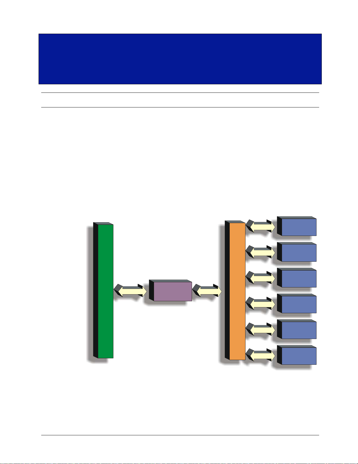
The SMP7500 is a member of the VXI Technology SMIP II™ (Switch Modularity Instrumentation
Platform) family and is available as a 96-channel, single SMIP Plug-In Module. As many as six
SMP7500s may be configured in a single double-slot VXI module, and 2 in a single-wide VXI
module. This would allow as many as 576 for a double-wide or 192 digital I/O for a single-wide
VXI Module. In addition, the SMP7500 may be combined with any of the other members of the
SMIP family to form a customized and highly integrated instrument/switch test solution. This
allows the user to reduce system size and cost by combining the SMP7500 with another
instrument/switch function in a single wide, C-size VXIbus module.
I
N
T
V
X
I
B
SMIP
INTERFACE
U
S
IGURE 1-1: SMIP™ SWITCH MODULARITY INSTRUMENTATION PLATFORM
F
E
R
N
L
S
M
I
P
B
U
S
SMIP SWITCH
MODULE #1
SMIP SWITCH
MODULE #2
SMIP SWITCH
MODULE #3
SMIP SWITCH
MODULE #4
SMIP SWITCH
MODULE #5
SMIP SWITCH
MODULE #6
SMP7500 Introduction 11
Artisan Technology Group - Quality Instrumentation ... Guaranteed | (888) 88-SOURCE | www.artisantg.com
VXI Technology, Inc.
Regardless of whether the SMP7500 is configured with other SMP7500 modules or with other
SMIP II modules, each group of 96 channels is treated as an independent plug-in in the SMIP II
module and as such, each group has its own FAIL/POWER and ACCESS/ERROR indicators.
M
M
M
O
D
U
L
E
#0
M
O
D
U
L
E
#1
M
O
D
U
L
E
#2
M
O
D
U
L
E
#5
O
O
D
D
U
U
L
L
E
E
#0
#1
M
M
O
O
D
D
U
U
L
L
E
E
#3
#4
FEATURES
DESCRIPTION
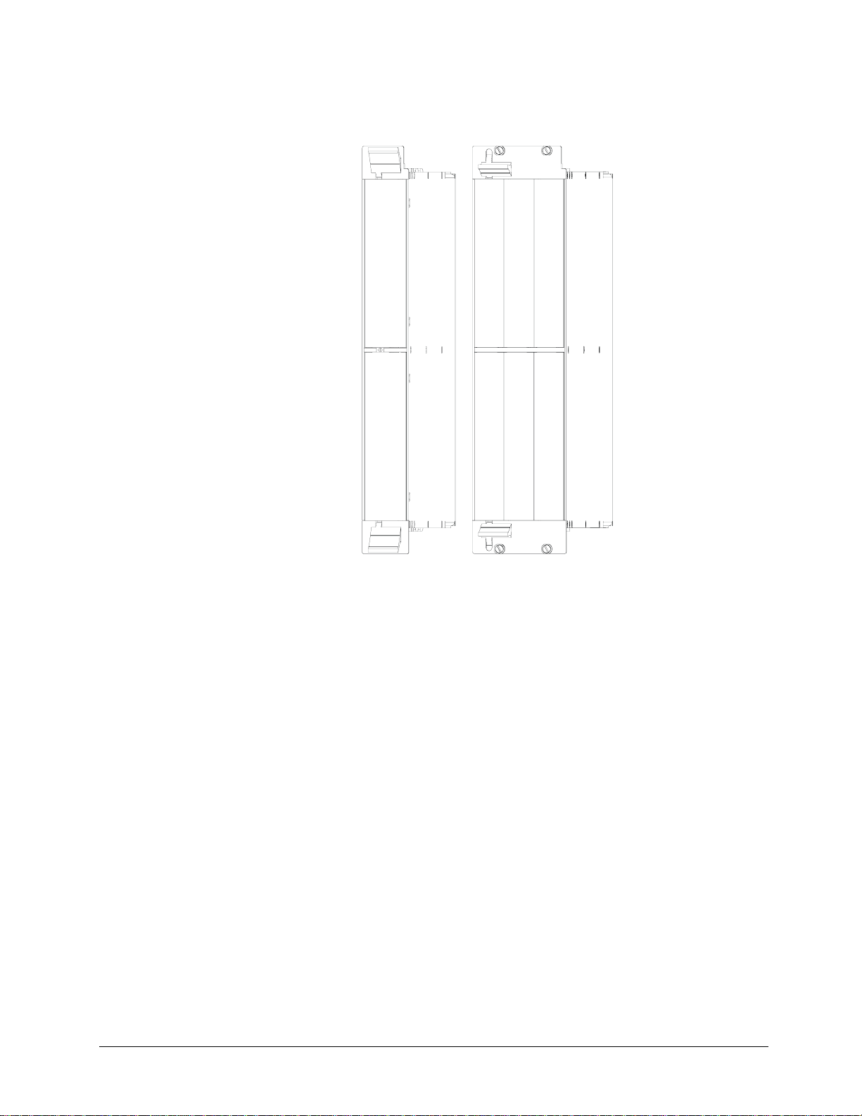
SMP1100 SMP1200
F
IGURE 1-2: FRONT PANEL LAYOUT
• 96 Channels, 12 groups of 8 bits. Up to 576 channels in a double-slot C-size card, up to
192 channels in a single C-size card.
• Group-wise programmable, as an input or an output, through user TTL input or VXI A24/32
registers.
• Group-wise programmable polarity through VXI A24/32 registers as an active high or low.
• Input: 0 V to 60 V, V
• Output: Open collector (N-DMOS), 0 V to 60 V, up to 300 mA continuous with over-voltage
and over-current protection.
• Data throughput: 5 µs typical system speeds, 200 kilobytes per second (kb/s) using D8 access,
400 kb/s using D16 access.
• Data Input/Output Clock Sources: For each group, from Front Panel (F/P) clock input, or VXI
Register Writes.
• Capture clock edge programmable as rising edge or falling edge.
• Register based data access for fast throughput.
The SMP7500 Open Collector Digital I/O module is a high performance I/O module that has been
designed for high voltage, current and data throughput. The instrument uses direct register access
for very high-speed data through-put.
IN (high)
≥ 2.0 V, V
≤ 1.5 V, input impedance ≥ 65 kΩ.
IN(low)
12 SMP7500 Introduction
Artisan Technology Group - Quality Instrumentation ... Guaranteed | (888) 88-SOURCE | www.artisantg.com

www.vtiinstruments.com
A single SMP7500 provides 96 open collector digital I/O line that are configurable as inputs or
outputs in twelve groups of 8 channels each. The module can drive up to 60 V with sink current of
up to 300 mA per channel. Each group of 8 bits is referred as a PORT. Each PORT can be
configured as an input port or an output port under program control. The SMP7500 has the
flexibility to configure the sourcing of the input and output clocks from either the front panel (F/P
GND_I/O) (one input per PORT), or via a VXI A24/A32 control register. There is also a Global
Clock Line from the front panel that may be user selected via hardware jumpers to drive selected
PORT clocks. By using the appropriate clocking configuration, very large numbers of channels
may by synchronized to collect or present data to a UUT (unit under test).
Each clock input is internally pulled to a logic high level and has an RC termination network to
reduce multiple clocking edges due to line ringing. The RC network consists of a 120 Ω resistor in
series with a 100 pF capacitor, giving a time constant of 12 ns.
The SMP7500 can be combined with any member of the SMIP II family to form a customized and
highly integrated instrument/switch.
SMP7500 Introduction 13
Artisan Technology Group - Quality Instrumentation ... Guaranteed | (888) 88-SOURCE | www.artisantg.com
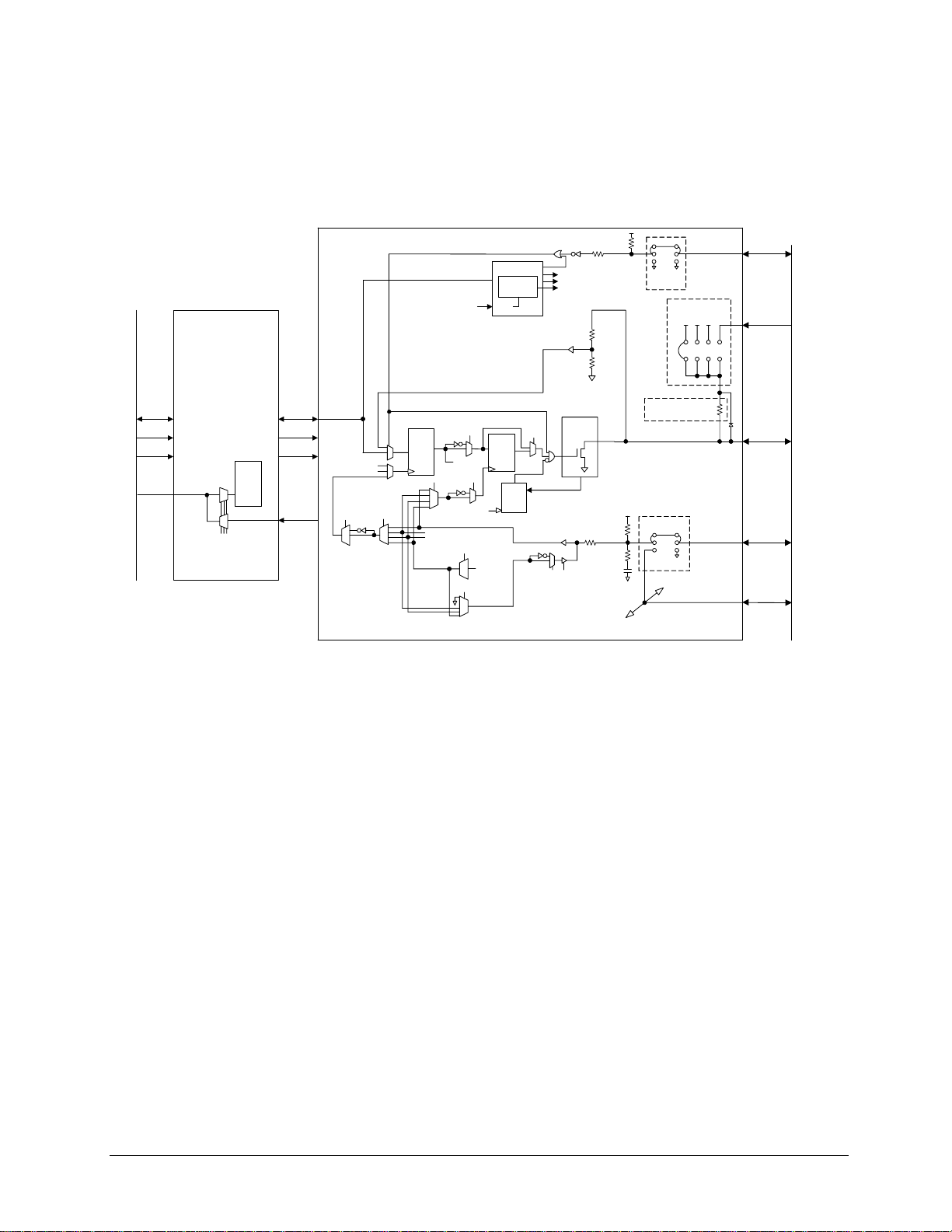
PROGRAMMING AND DATA ACCESS
Register-based Data Access: The I/O ports are directly mapped into the VXI user
SMIP INTERFACE
MODULE
DATA
ADDRESS
CONTROL
BUSYN
Backplane Load
Transparent
Polarity
ADDRESS
CONTROL
VXI BACKPLANE
DATA
TTL
TRIGGER
BUS
0-7
Control
Trace
Memory
Control
I/O Data
Buffer
Data
WR Event
Relay Req. 000Ch Write Event
SMP7500 MODULE
Control
R/B
Polarity
Latched
Output
Data
Buffer
R/B
PolarityControl
Over Current
Reset
Control
All Other
Available F/P
CLK Lines
Control
VXI Technology, Inc.
definable registers in the A24 or A32 address space.
Data access occurs in approximately 500 ns,
depending on the controller and software used.
USER CONNECTOR
GND_I/O
CLAMP
Fly Back Protection Diode
DATA
GND_CLK
GLOBAL
CLK
Control
Writes to
Specific Port
Addresses
Over
Current
Sense /
Control
Immediate
Double
Buffered
Over Current Sense
Shut Down
Control
Relay Req. 000Ch Write Event
WR EVENT
Output
Drivers
ISENSE
2
2
Polarity Enable
47k
22
200K
33K
47K
120
100pf
User Selectable
HW Jumpers
User Selectable
HW Jumpers
+5V +12V +24V
User Configurable 100K
Pull-Up Resistor Network (SIP)
User Selectable
HW Jumpers
Off To All Other Ports
F
IGURE 1-3: SMP7500 MODULE BLOCK DIAGRAM
14 SMP7500 Introduction
Artisan Technology Group - Quality Instrumentation ... Guaranteed | (888) 88-SOURCE | www.artisantg.com

www.vtiinstruments.com
SMP7500 SPECIFICATIONS
GENERAL SPECIFICATIONS
NUMBER OF CHANNELS
DIRECTION
DATA ACCESS TYPES
DATA THROUGHPUT
PHYSICAL INTERFACE
CHANNEL INPUT CHARACTERISTICS
V
V
V
IN(high)
IN(low)
IN(max)
Input Impedance
CHANNEL OUTPUT CHARACTERISTICS
V
OUT(max)
Current Sink (Maximum)
Switch On Time
CLOCK AND CONTROL INPUT CHARACTERISTICS
V
V
IN(high)
IN(low)
Current In (VIN = 5.0 V)
DATA INPUT CLOCK SOURCES
DATA OUTPUT CLOCK SOURCES
TTL TRIGGER OUTPUT SOURCES
CLOCKED INPUT DATA HOLD
POWER REQUIREMENTS
COOLING REQUIREMENTS
96 (12 groups of 8 bits)
Selectable as input or output
Direct register access
5 µs typical system (500 µs register cycle time)
200 kb/s using D8 access
400 kb/ using D16 access
N channel DMOS transistor (TPIC2601KTC for rev. A PCBs, STS4DNF60L
for Rev. B or higher) with a current protection circuit on the output side, and a
voltage divider and voltage comparator on the input side
≥ 2.0 V
≤ 1.5 V
≤ 60 V
≥ 65 kΩ
≤ 60 V
≤ 300 mA
≤ 1 µs
> 2.0 V
< 0.8 V
< 10 µA
12 Front Panel, plus 1 Global Clock, A24/A32 Register Write
12 Front Panel, A24/A32 Register Write
Board Busyn controlled
≥ 2 µs
+5 V @ 864 mA, +12 V @ 60 mA
0.4 L/s
SMP7500 Introduction 15
Artisan Technology Group - Quality Instrumentation ... Guaranteed | (888) 88-SOURCE | www.artisantg.com

VXI Technology, Inc.
16 SMP7500 Introduction
Artisan Technology Group - Quality Instrumentation ... Guaranteed | (888) 88-SOURCE | www.artisantg.com

www.vtiinstruments.com
SECTION 2
PREPARATION FOR USE
INTRODUCTION
When the SMP7500 is unpacked from its shipping carton, the contents should include the
following items:
(1) SMP7500 VXIbus module
(1) SMP7500 Open Collector Digital I/O Module User’s Manual (this manual)
All components should be immediately inspected for damage upon receipt of the unit.
Once the SMIP II is assessed to be in good condition, it may be installed into an appropriate C-
size or D-size VXIbus chassis in any slot other than slot zero. The chassis should be checked to
ensure that it is capable of providing adequate power and cooling for the SMIP II. Once the
chassis is found adequate, the SMIP II’s logical address and the chassis’ backplane jumpers
should be configured prior to the SMIP II’s installation.
CALCULATING SYSTEM POWER AND COOLING REQUIREMENTS
It is imperative that the chassis provide adequate power and cooling for this module. Referring to
the chassis operation manual, confirm that the power budget for the system (the chassis and all
modules installed therein) is not exceeded and that the cooling system can provide adequate
airflow at the specified backpressure.
It should be noted that if the chassis cannot provide adequate power to the module, the instrument
might not perform to specification or possibly not operate at all. In addition, if adequate cooling is
not provided, the reliability of the instrument will be jeopardized and permanent damage may
occur. Damage found to have occurred due to inadequate cooling could also void the warranty of
the module.
SETTING THE CHASSIS BACKPLANE JUMPERS
Please refer to the chassis operation manual for further details on setting the backplane jumpers.
SMP7500 Introduction 17
Artisan Technology Group - Quality Instrumentation ... Guaranteed | (888) 88-SOURCE | www.artisantg.com

SETTING THE LOGICAL ADDRESS
The logical address of the SMIP II is set by two rotary switches located on the top edge of the
interface card, near the backplane connectors. Each switch is labeled with positions 0 through F.
The switch closer to the front panel of the module is the least significant bit (LSB or “Front”),
and the switch located towards the back of the module is the most significant bit (MSB or
“Back”). To set the Logical Address (LA), simply rotate the pointer to the desired value. For
example, to set the LA to 25, first convert the decimal number to the hexadecimal value of 19.
Next, set the back switch to 1, and the front switch to 9. See
conversion examples:
Example 1
VXI Technology, Inc.
Figure 2-1. Here are a couple of
LA
(decimal)
Divide
by 16
MSB LSB
25 25 / 16 = 1 w/ 9 remaining Divide the decimal value by 16 to get
the MSB and the LSB.
= 0001 1001 The 1 is the MSB, and the remainder of
9 is the LSB.
= 1 9 Convert to hexadecimal. Set the back
switch to 1 and the front switch to 9.
BACK FRONT
5
4
6
3
2
1
0
F
F
IGURE 2-1: LOGICAL ADDRESS EXAMPLE 1
7
8
9
A
B
E
C
D
Here is another way of looking at the conversion: LA = (back switch x 16) + front switch
LA = (1 x 16) + 9
LA = 16 + 9
LA = 25
4
5
6
3
2
1
0
F
7
8
9
A
B
E
C
D
18 SMP7500 Programming
Artisan Technology Group - Quality Instrumentation ... Guaranteed | (888) 88-SOURCE | www.artisantg.com

www.vtiinstruments.com
Example 2
LA
(decimal)
Divide
by 16
MSB LSB
200 200 / 16 = 12 w/ 8 remaining Divide by 16.
= 1100 1000 Convert to MSB and LSB.
= C 8 Convert to hexadecimal. Set the back
switch to C and the front switch to 8.
BACK FRONT
5
4
6
3
2
1
0
F
F
IGURE 2-2: LOGICAL ADDRESS EXAMPLE 2
7
8
9
A
B
E
C
D
Set the address switches to FF (factory default) for dynamic configuration. Upon power-up, the
resource manager will assign a logical address. See Section F - Dynamic Configuration in the
VXIbus Specification for further information.
There is only one logical address per SMIP II base unit. Address assignments for individual
modules are handled through the A24/A32 address space allocation.
4
5
6
3
2
1
0
F
7
8
9
A
B
E
C
D
SELECTING THE EXTENDED MEMORY SPACE
The Extended Memory Space of the SMIP II is set by a dip-switch that is located on the bottom
edge of the interface card. Position 1, located to the left on the dip-switch, selects between A24
and A32 memory address space. In the UP position, the SMIP II will request A24 space. In the
DOWN position, the SMIP II will request A32 space. (Position 2 is not currently used.) The
selection of the address space should be based upon the memory allocation requirements of the
system that the SMIP II module will be installed. The amount of memory allocated to the SMIP II
module is independent of the address space selected.
SMP7500 Programming 19
Artisan Technology Group - Quality Instrumentation ... Guaranteed | (888) 88-SOURCE | www.artisantg.com

FRONT PANEL INTERFACE WIRING
The SMP7500’s module interface is made available on the front panel of the instrument. The
160-pin connector contains all of the signals available for this instrument. The connector used on
the SMP7500 is a readily available 160-pin 5 row DIN type connector. Many mating options are
available for this connector style, anything from crimp-and-poke to screw terminal connections.
Several cable shroud options are also available.
ABLE 2-1: J100 PIN OUTS
T
VXI Technology, Inc.
ROW
A
1 DATA0.0 1 DATA2.0 1 DATA4.0 1 CLAMP0 1 CLAMP1
2 DATA0.1 2 DATA2.1 2 DATA4.1 2 GND/CLK0 2 GND/CLK1
3 DATA0.2 3 DATA2.2 3 DATA4.2 3 GND/IO0 3 GND/IO1
4 DATA0.3 4 DATA2.3 4 DATA4.3 4 GND 4 GND
5 DATA0.4 5 DATA2.4 5 DATA4.4 5 CLAMP2 5 CLAMP3
6 DATA0.5 6 DATA2.5 6 DATA4.5 6 GND/CLK2 6 GND/CLK3
7 DATA0.6 7 DATA2.6 7 DATA4.6 7 GND/IO2 7 GND/IO3
8 DATA0.7 8 DATA2.7 8 DATA4.7 8 GND 8 GND
9 DATA1.0 9 DATA3.0 9 DATA5.0 9 CLAMP4 9 CLAMP5
10 DATA1.1 10 DATA3.1 10 DATA5.1 10 GND/CLK4 10 GND/CLK5
11 DATA1.2 11 DATA3.2 11 DATA5.2 11 GND/IO4 11 GND/IO5
12 DATA1.3 12 DATA3.3 12 DATA5.3 12 GND 12 GND
13 DATA1.4 13 DATA3.4 13 DATA5.4 13 CLAMP6 13 CLAMP7
14 DATA1.5 14 DATA3.5 14 DATA5.5 14 GND/CLK6 14 GND/CLK7
15 DATA1.6 15 DATA3.6 15 DATA5.6 15 GND/IO6 15 GND/IO7
16 DATA1.7 16 DATA3.7 16 DATA5.7 16 GND 16 GND
17 DATA6.0 17 DATA8.0 17 DATA10.0 17 CLAMP8 17 CLAMP9
18 DATA6.1 18 DATA8.1 18 DATA10.1 18 GND/CLK8 18 GND/CLK9
19 DATA6.2 19 DATA8.2 19 DATA10.2 19 GND/IO8 19 GND/IO9
20 DATA6.3 20 DATA8.3 20 DATA10.3 20 GND 20 GND
21 DATA6.4 21 DATA8.4 21 DATA10.4 21 CLAMP10 21 CLAMP11
22 DATA6.5 22 DATA8.5 22 DATA10.5 22 GND/CLK 10 22 GND/CLK 11
23 DATA6.6 23 DATA8.6 23 DATA10.6 23 GND/IO10 23 GND/IO11
24 DATA6.7 24 DATA8.7 24 DATA10.7 24 GND 24 GND
25 DATA7.0 25 DATA9.0 25 DATA11.0 25 GND 25 GND/GCLK
26 DATA7.1 26 DATA9.1 26 DATA11.1 26 GND 26 GND
27 DATA7.2 27 DATA9.2 27 DATA11.2 27 GND 27 GND
28 DATA7.3 28 DATA9.3 28 DATA11.3 28 GND 28 GND
29 DATA7.4 29 DATA9.4 29 DATA11.4 29 GND 29 GND
30 DATA7.5 30 DATA9.5 30 DATA11.5 30 GND 30 GND
31 DATA7.6 31 DATA9.6 31 DATA11.6 31 GND 31 GND
32 DATA7.7 32 DATA9.7 32 DATA11.7 32 GND 32 GND
SIGNAL
ROW
B
SIGNAL
ROW
C
SIGNAL
ROW
D
SIGNAL
ROW
E
SIGNAL
20 SMP7500 Programming
Artisan Technology Group - Quality Instrumentation ... Guaranteed | (888) 88-SOURCE | www.artisantg.com

www.vtiinstruments.com
HARDWARE JUMPER SELECTION
The SMP7500 module contains many user selectable hardware jumpers. The jumpers are of the
2-pin finger removable type found on most personal computers and hard disk drives. These
jumpers set the fly-back protection voltage, the functionality of the front panel (F/P) GND_I/O,
GND_CLK and Global CLK lines, as well as the direction of the PORTs. The
shows the appropriate jumper settings for the module setup desired.
Front Panel CLAMP Lines
The F/P CLAMP lines are available for user defined voltages that are to be used to suppress
inductive fly-back transients on the PORT lines. This helps protect other circuitry on the PORT’s
data lines from an over-voltage condition. The F/P CLAMP line is only one of several sources that
may be selected to drive the fly-back protection diodes that are installed on the module. Hardware
selectable jumpers on the module can also be used to select either +24 V dc, +12 V dc, or
+5 V dc. The voltage selected is routed to the cathode of a fly-back protection diode, whose anode
is then connected to the associated PORT’s data line. Every PORT data line has a fly-back
protection diode installed. If no protection voltage is desired, simply hardware jumper the clamp
voltage to the F/P CLAMP line and do not connect that lin e to any voltage.
Front Panel GND_I/O Lines
The F/P GND_I/O lines may be configured as either GrouND, or an input line that controls the
direction of the associated PORT. If used as inputs the F/P GND_I/O lines are pulled-up to +5 V
via a 47 kΩ resistor. If these lines are configured as input control lines and are not driven low,
they will pull-up setting the associated port as an input. If pulled low, they will set the port to an
output. All F/P GND_I/O lines may be overridden either by a hardware jumper setting or
programmatically to set the port direction to output.
Table 2-2 below
If set to GrouND, these lines can be used as additional user employable Ground pins to the
module. This increases the user attachments to the system’s ground. For high speed switching of
many simultaneous channels it may be necessary to use these pins as ground in order to reduce
signal bounce caused by switching transients. If these lines are used as GND, and they are not
overridden, then they are internally pulled-up and set the PORT’s direction as input.
There are two ways to override the F/P GND_I/O lines. A hardware jumper may be used to select
the PORT as an output, or the PORT may be programmatically set to an output. If these lines are
overridden, then they have no effect on the module.
Front Panel GND_CLK Lines
The F/P GND_CLK lines may be configured as either GrouND, an input line, or an output line
that controls data capture of the associated PORT. If used as inputs the F/P GND_CLK lines are
pulled-up to +5 V via a 47 kΩ resistor. There is as well a network of a 120 Ω resistor in series
with a 100 pF capacitor for termination of the F/P_CLK lines. The polarity of the clock lines are
programmable as well.
If set to GrouND, they can be used as additional user employable Ground pins to the module. This
increases the user attachments to the system’s ground. For high speed switching of many
simultaneous channels it may be necessary to use these pins as ground in order to reduce signal
bounce caused by switching transients.
A Global CLK Line is available on the front panel. This line is to be used to gang several, or all,
PORT clock lines into a single source/destination. The Global CLK line is routed to the required
PORTs via hardware jumpers. If a PORT is configured to use the Global CLK line, then its
associated F/P GND_CLK line has no effect on the module.
SMP7500 Programming 21
Artisan Technology Group - Quality Instrumentation ... Guaranteed | (888) 88-SOURCE | www.artisantg.com

HARDWARE RESISTOR NETWORK PULL-UP SELECTION
The SMP7500 module contains user selectable hardware resistor networks that are used to pull-up
the F/P data lines to the selected CLAMP voltage. The networks are of the 9-pin 8-resistor singlein-line (SIP) type. Examples of this type of resistor network are:
Dale Electronics, Inc CSC09A01104G (100 kΩ)
BI Technologies BH9-1104 (100 kΩ)
VXI Technology, Inc.
RR R R R R R R
Pin 1
Pin 2Pin 3Pin 4Pin 5Pin 6Pin 7Pin 8Pin 9
F
IGURE 2-3: RESISTOR NETWORK 9P8R SIP
The values of these resistor networks may be selected and the networks replaced per customer
requirements. Care should be taken to follow the power rating of the networks selected and the
application voltage used so as not to create a potenially dangerous situation. VXI Technology,
Inc. does not carry other values of these resistor networks.
Front Panel CLAMP Lines
The F/P CLAMP lines are available for user defined voltages that are to be used to suppress
inductive fly-back transients on the PORT lines. This helps protect other circuitry on the PORT’s
data lines from an over-voltage condition. The F/P CLAMP line is only one of several sources that
may be selected to drive the fly-back protection diodes that are installed on the module. Hardware
selectable jumpers on the module can also be used to select either +24 VDC, +12 VDC, or
+5 VDC. The voltage selected is routed to the cathode of a fly-back protection diode, whose
anode is then connected to the associated PORT’s data line. Every PORT data line has a fly-back
protection diode installed. If no protection voltage is desired, simply hardware jumper the clamp
voltage to the F/P CLAMP line and do not connect that lin e to any voltage.
22 SMP7500 Programming
Artisan Technology Group - Quality Instrumentation ... Guaranteed | (888) 88-SOURCE | www.artisantg.com

www.vtiinstruments.com
TABLE 2-2: HARDWARE JUMPER CONFIGURATION
HARDWARE JUMPERS INSTALLED (HW = HARD WIRED via JUMPER)
FUNCTION PORT 0 PORT 1 PORT 2 PORT 3 PORT 4 PORT 5
GND_I/O = GND J1 – 1 to 2 J7 – 1 to 2 J14 – 1 to 2 J11 – 1 to 2 J22 – 1 to 2 J19 – 1 to 2
GND_I/O = I/0 * J1 – 2 to 3
J2 – 2 to 3
J7 – 2 to 3
J6 – 2 to 3
J14 – 2 to 3
J13 – 2 to 3
J11 – 2 to 3
J10 – 2 to 3
J22 – 2 to 3
J21 – 2 to 3
J19 – 2 to 3
J18 – 2 to 3
PORT HW AS OUTPUT * J2 – 1 to 2 J6 – 1 to 2 J13 – 1 to 2 J10 – 1 to 2 J21– 1 to 2 J18– 1 to 2
GND_CLK = GND J3 – 1 to 2 J5 – 1 to 2 J12 – 1 to 2 J9 – 1 to 2 J20 – 1 to 2 J17 – 1 to 2
GND_CLK = INPUT OR
OUTPUT *
J3 – 2 to 3
J4 – 1 to 2
J5 – 2 to 3
J8 – 1 to 2
J12 – 2 to 3
J15 – 1 to 2
J9 – 2 to 3
J16 – 1 to 2
J20 – 2 to 3
J23 – 1 to 2
J17 – 2 to 3
J24 – 1 to 2
GLOBAL CLK = INPUT * J4 – 2 to3 J8 – 2 to3 J15 – 2 to3 J16 – 2 to3 J23 – 2 to3 J24 – 2 to3
CLAMP = EXT * J49 – 1 to 2 J52 – 1 to 2 J55 – 1 to 2 J58 – 1 to 2 J61 – 1 to 2 J64 – 1 to 2
CLAMP = +24V * J49 – 2 to 3
J50 – 1 to 2
CLAMP = +12V * J49 – 2 to 3
J50 – 2 to 3
J51 – 1 to 2
CLAMP = +5V * J49 – 2 to 3
J50 – 2 to 3
J51 – 2 to 3
J52 – 2 to 3
J53 – 1 to 2
J52 – 2 to 3
J53 – 2 to 3
J54 – 1 to 2
J52 – 2 to 3
J53 – 2 to 3
J54 – 2 to 3
J55 – 2 to 3
J56 – 1 to 2
J55 – 2 to 3
J56 – 2 to 3
J57 – 1 to 2
J55 – 2 to 3
J56 – 2 to 3
J57 – 2 to 3
J58 – 2 to 3
J59 – 1 to 2
J58 – 2 to 3
J59 – 2 to 3
J60 – 1 to 2
J58 – 2 to 3
J59 – 2 to 3
J60 – 2 to 3
J61 – 2 to 3
J62 – 1 to 2
J61 – 2 to 3
J62 – 2 to 3
J63 – 1 to 2
J61 – 2 to 3
J62 – 2 to 3
J63 – 2 to 3
J64 – 2 to 3
J65 – 1 to 2
J64 – 2 to 3
J65 – 2 to 3
J66 – 1 to 2
J64 – 2 to 3
J65 – 2 to 3
J66 – 2 to 3
HARDWARE JUMPERS INSTALLED (HW = HARD WIRED via JUMPER)
FUNCTION PORT 6 PORT 7 PORT 8 PORT 9 PORT 10 PORT 11
GND_I/O = GND J33 – 1 to 2 J31 – 1 to 2 J29 – 1 to 2 J45 – 1 to 2 J39 – 1 to 2 J37 – 1 to 2
GND_I/O = I/0 * J33 – 2 to 3
J32 – 2 to 3
J31 – 2 to 3
J30 – 2 to 3
J29 – 2 to 3
J28 – 2 to 3
J45 – 2 to 3
J44 – 2 to 3
J39 – 2 to 3
J38 – 2 to 3
J37 – 2 to 3
J36 – 2 to 3
PORT HW AS OUTPUT * J32 – 1 to 2 J30 – 1 to 2 J28 – 1 to 2 J44 – 1 to 2 J38– 1 to 2 J36– 1 to 2
GND_CLK = GND J35 – 1 to 2 J26 – 1 to 2 J47 – 1 to 2 J46 – 1 to 2 J41 – 1 to 2 J40 – 1 to 2
GND_CLK = INPUT OR
OUTPUT *
J35 – 2 to 3
J34 – 1 to 2
J26 – 2 to 3
J27 – 1 to 2
J47 – 2 to 3
J25 – 1 to 2
J46 – 2 to 3
J48 – 1 to 2
J41 – 2 to 3
J42 – 1 to 2
J40 – 2 to 3
J43 – 1 to 2
GLOBAL CLK = INPUT * J34 – 2 to3 J27 – 2 to3 J25 – 2 to3 J48 – 2 to3 J42 – 2 to3 J43 – 2 to3
CLAMP = EXT * J73 – 1 to 2 J67 – 1 to 2 J70 – 1 to 2 J76 – 1 to 2 J79 – 1 to 2 J82 – 1 to 2
CLAMP = +24V * J73 – 2 to 3
J74 – 1 to 2
CLAMP = +12V * J73 – 2 to 3
J74 – 2 to 3
J75 – 1 to 2
CLAMP = +5V * J73 – 2 to 3
J74 – 2 to 3
J75 – 2 to 3
J67 – 2 to 3
J68 – 1 to 2
J67 – 2 to 3
J68 – 2 to 3
J69 – 1 to 2
J67 – 2 to 3
J68 – 2 to 3
J69 – 2 to 3
J70 – 2 to 3
J71 – 1 to 2
J70 – 2 to 3
J71 – 2 to 3
J72 – 1 to 2
J70 – 2 to 3
J71 – 2 to 3
J72 – 2 to 3
J76 – 2 to 3
J77 – 1 to 2
J76 – 2 to 3
J77 – 2 to 3
J78 – 1 to 2
J76 – 2 to 3
J77 – 2 to 3
J78 – 2 to 3
J79 – 2 to 3
J80 – 1 to 2
J79 – 2 to 3
J80 – 2 to 3
J81 – 1 to 2
J79 – 2 to 3
J80 – 2 to 3
J81 – 2 to 3
J82 – 2 to 3
J83 – 1 to 2
J82 – 2 to 3
J83 – 2 to 3
J84– 1 to 2
J82 – 2 to 3
J83 – 2 to 3
J84 – 2 to 3
SMP7500 Programming 23
Artisan Technology Group - Quality Instrumentation ... Guaranteed | (888) 88-SOURCE | www.artisantg.com

VXI Technology, Inc.
24 SMP7500 Programming
Artisan Technology Group - Quality Instrumentation ... Guaranteed | (888) 88-SOURCE | www.artisantg.com

www.vtiinstruments.com
SECTION 3
PROGRAMMING
INTRODUCTION
The SMP7500 is accessed like any other SMIP II plug-in module. Although its register map is
slightly different than that of the switch control maps of the other SMIP plug-in modules.
References to switch, relay, or port registers are all terms used to describe the same hardware
registers contained on this module. The standard SMIP II Switch modules use the PORT registers
on this module as relay/switch registers.
REGISTER ACCESS
ADDRESSING
The SMIP II modules are VXIbus register-based devices for high-speed data retrieval. Registerbased programming is a series of reads and writes directly to the switch module registers. This
eliminates the time for command parsing thus increasing speed.
The VTI switching modules utilize either the A24 or A32 space of the shared-memory
architecture. To read or write to a module register, a register address needs to be specified. This is
done by using the offset value (assigned by the resource manager) and multiplying it by 256 or
64 k to get the base address in A24 or A32 address space, respectively
A24 Base Address = Offset value * 0x00FF (or 256)
A32 Base Address = Offset value * 0xFFFF (or 65,535)
The A24 or A32 offset value, assigned by the resource manager, can also be accessed by reading
the A16 Offset Register. To address the A16 Offset Register use the following formula:
A16 Base Address = (Logical Address * 64) + 0xC000 (or 49,152)
then
A16 Offset Register Address = A16 Base Address + 6
See following for the A16 Memory Map and the A24/A32 address space allocation.
SMP7500 Programming 25
Artisan Technology Group - Quality Instrumentation ... Guaranteed | (888) 88-SOURCE | www.artisantg.com

VXI Technology, Inc.
TABLE 3-1: SMIP II REGISTER MAP - A16
OFFSET WRITE FUNCTION READ FUNCTION
3E Trace Advance Board Busy
3C Busy Trigger Control Busy Trigger Control
3A Trace RAM Control Trace RAM Control
38 TTL Trigger Polarity Reserved
36 Open Trigger Select Reserved
34 Trace ADV Trigger Select Reserved
32 Trace RAM Address LOW Trace RAM Address LOW
30 Trace RAM Address HIGH Trace RAM Address HIGH
2E Trace RAM End LOW Trace RAM End LOW
2C Trace RAM End HIGH Trace RAM End HIGH
2A Trace RAM Start LOW Trace RAM Start LOW
28 Trace RAM Start HIGH Trace RAM Start HIGH
26 Module 5, 4 Used Address Reserved
24 Module 3, 2 Used Address Reserved
22 Module 1, 0 Used Address Reserved
20 NVM Access Register NVM Access Register
1E Reserved Subclass Register
1C Interrupt Control Interrupt Control
1A Reserved Interrupt Status
18 Reserved Reserved
16 Reserved Reserved
14 Reserved Reserved
12 Reserved Reserved
10 Reserved Reserved
E Reserved Version Number
C Reserved Serial Number LOW
A Reserved Serial Number HIGH
8 Reserved Reserved
6 Offset Register Offset Register
4 Control Register Status Register
2 Reserved Device Type Register
0 LA Register ID Register
26 SMP7500 Programming
Artisan Technology Group - Quality Instrumentation ... Guaranteed | (888) 88-SOURCE | www.artisantg.com
www.vtiinstruments.com
DESCRIPTION OF REGISTERS - A16
The following describes the registers shown in the SMIP II Register Map for A16 address space.
ID Register- Read Only
D11-D0 Manufacturer's ID VXI Technology, Inc., set to F4B
D13-D12 Address Space
A16/A24
A16/A32 = 012
D15-D14 Device Class Extended register based device, set to 01
Logical Address Register - Write Only
Sets the new logical address in a dynamically configured module.
D7-D0 Logical Address
When set for dynamic configuration (set to FF
alter the configured logical address, while a hard reset will set the
register back to FF
D15-D8 Reserved Writing to this range has no effect.
Device Type Register - Read Only
D11-D0 Model Code Model 277, set to 115
D15-D12 Required Memory
2 Mbytes, set to 2
2 Mbytes, set to A
Status Register - Read Only
D15 A24/A32 Active
D14 MODID*
D13-D4 Reserved These bits always read as 11,1111,11112
D3 Ready This bit always reads as 12
D2 Passed This bit always reads as 12
D1-D0 Reserved These bits always read as 112
1 = indicates that A24/A32 memory space access is enabled
0 = indicates that A24/A32 memory space access is locked out
1 = indicates that the module is not selected by the MODID line
0 = indicates that the module is selected by the MODID line.
Control Register - Write Only
D15 A24/A32 Enable
D14-D2 Reserved Writes to these bits have no effect.
D1 Sysfail Inhibit
D0 Reset
1 = write a 1 to this bit to enable A24/A32 memory access
0 = to disable access
Write a 1 to this bit to prevent the module from asserting the
SYSFAIL* line.
1 = write a 1 to this bit to force the registers on the SMIP II interface
board into a reset state
0 = write a 0 to release this soft reset state
Note: This does not reset relays on the SMIP II plug-in modules.
= 00
2
.
16
16
, for A24
16
, for A32
16
16
2
) a soft reset will not
16
SMP7500 Programming 27
Artisan Technology Group - Quality Instrumentation ... Guaranteed | (888) 88-SOURCE | www.artisantg.com

VXI Technology, Inc.
Offset Register - Read and Write
The value written to this 16-bit register, times 256, sets the base
address of the A24 memory space used by the module. The value
written to this 16-bit register, times 65,536, sets the base address of
D15-D0 A24/A32 Memory Offset
the A32 memory space used by the module. A read from this register
reflects the previously written value. Because of the required
memory size, bits D4-D0 are disregarded on writes and always read
back as 0s. Upon receiving a hard reset, all bits in this register are set
to 0s. A soft reset does not effect the value in this register.
Serial Number High Register- Read Only
D15-D0 Not Implemented Always read back as FFFF
16
Serial Number Low Register - Read Only
D15-D0 Not Implemented Always read back as FFFF
16
Version Number Register - Read Only
D15-D8
D7-D4
D3-D0
Firmware Version
Number
Major Hardware Version
Number
Minor Hardware Version
Number
Not applicable, reads back as FF
16
Depends on the specific hardware revision of the SMIP II interface
board.
Depends on the specific hardware revision of the SMIP II interface
board.
Interrupt Status Register - Read Only
D15 Scan Function done The latest scan list update is complete.
D14
Openbus Active Event
true
The Openbus was activated by one or more programmed inputs. See
description of the Openbus in the module register section.
D13 = Module 5 …, and D8 = Module 0.
The programmed Busy signal from one of the modules has timed
out. This indicates that the relays actuated for that Busy cycle have
D13-D8
Modules 0-5 Busy
complete
settled and a measurement may take place.
D7-D0 Reserved Always reads back as FF
16
Note: This status register may be used in a polled fashion rather than allowing the events above to generate an
Interrupt. A read of this register will clear any active bits. Bits that are not set, or are about to be set, are
not effected by a read of this register.
28 SMP7500 Programming
Artisan Technology Group - Quality Instrumentation ... Guaranteed | (888) 88-SOURCE | www.artisantg.com

www.vtiinstruments.com
Interrupt Control Register - Read and Write
D15
D14
D13-D8
Scan Function done mask
bit
Openbus Active Event
true mask bit
Module 0-5 Busy
complete
D7 IR ENA*
D6 IH ENA*
D5-D3 Interrupter IRQ Line
D2-D0 Handler IRQ Line
Note that all bits in this register are set to 1s upon receipt of a hard or soft reset.
0 = enabled
1 = disabled
0 = enabled
1 = disabled
0 = enabled
1 = disabled
D13 = Module 5,… and D8 = Module 0.
0 = writing a 0 to this bit enables interrupter capabilities
1 = writing a 1 to this bit disables interrupter capabilities
The module has no interrupt handler capability, therefore writing a 1
or 0 has no effect. A 1 is always read back for this bit.
The complement of the value programmed into these three bits
reflects the selected IRQ line used by the module. A value of 011
would select IRQ4, a value of 000
would disconnect the IRQ lines.
of 111
2
would select IRQ7, and a value
2
The module has no interrupt handler capability; therefore writing to
these bits has no effect. A 111
is always read back for these bits.
2
Subclass Register - Read Only
D15 VXIbus Extended Device Always reads as 1.
D14-D0 Extended Memory Device Always reads as 7FFD
16
NVM Access Register - Read
D15-D1 Unused All Bits are always 1.
D0
Reads back the serial data stream from the selected SMIP II board.
Note that only one SMIP II board may be read back at a time.
NVM Access Register - Write
D15-D7 Unused Data written to these bits have no effect.
D6 Serial clock for module 5; should be a logic 1 when not used.
D5 Serial clock for module 4; should be a logic 1 when not used.
D4 Serial clock for module 3; should be a logic 1 when not used.
D3 Serial clock for module 2; should be a logic 1 when not used.
D2 Serial clock for module 1; should be a logic 1 when not used.
D1 Serial clock for module 0; should be a logic 1 when not used.
D0 Serial data input for all modules; must be a logic 1 when not used.
Board X, Y Used Address Register - Read and Write
D15-D8
D7-D0
Sets the actual number of words of address space used by the relays
on board's X.
Sets the actual number of words of address space used by the relays
on board's Y.
Trace RAM Start High Register - Read and Write
D15-D4 Unused Data written to these bits have no effect and always read back as 1s.
D3-D0
Sets the four most significant bits of the starting address of the Trace
RAM, allowing the available RAM to be divided into multiple traces.
2
SMP7500 Programming 29
Artisan Technology Group - Quality Instrumentation ... Guaranteed | (888) 88-SOURCE | www.artisantg.com

VXI Technology, Inc.
Trace RAM Start Low Register - Read and Write
D15-D0
Sets the 16 least significant bits of the starting address of the Trace
RAM, allowing the available RAM to be divided into multiple traces.
Trace RAM End High Register - Read and Write
D15-D4 Unused Data written to these bits have no effect and always read back as 1s.
D3-D0
Sets the four most significant bits of the ending address of the Trace
RAM, allowing the available RAM to be divided into multiple traces.
Trace RAM End Low Register - Read and Write
D15-D0
Sets the 16 least significant bits of the ending address of the Trace
RAM, allowing the available RAM to be divided into multiple traces.
Trace RAM Address HIGH Register - Read and Write
D15-D4 Unused Data written to these bits have no effect and always read back as 1s.
Sets and reads back the four most significant bits of the current
D3-D0
address of the Trace RAM, allowing the current trace RAM address
to be queried and changed.
Trace RAM Address LOW Register - Read and Write
Sets and reads back the sixteen least significant bits of the current
D15-D0
address of the Trace RAM, allowing the current trace RAM address
to be queried and changed.
30 SMP7500 Programming
Artisan Technology Group - Quality Instrumentation ... Guaranteed | (888) 88-SOURCE | www.artisantg.com

www.vtiinstruments.com
Trace Advance Trigger Select Register - Write Only
Sets the TTLTRIG line or lines, which are configured as outputs, and
will toggle when Trace Advance condition occurs in the module.
D15-D8
D7-D0
D15 corresponds to TTLTRIG7, D14 to TTLTRIG6, … and D8 to
TTLTRIG0. Setting a bit to a 1 enables the trigger line, setting a bit
to 0 disables the corresponding line. All bits are set to 0s when either
a soft or a hard reset is received by the module.
Sets the TTLTRIG line or lines, which are configured as inputs, and
will cause a Trace Advance event to occur in the module. D7
corresponds to TTLTRIG7, D6 to TTLTRIG6, … and D0 to
TTLTRIG0. Setting a bit to a 1 enables the trigger line, setting a bit
to 0 disables the corresponding line. All enabled TTLTRIG lines are
or'd together to allow more than one TTLTRIG line to cause a Trace
Advance event to occur. All bits are set to 0s when the module
receives either a soft or a hard reset.
Open Trigger Select Register - Write Only
Sets the TTLTRIG line or lines, which are configures as outputs, and
will toggle when Relay Open condition occurs in the module. D15
D15-D8
D7-D0
corresponds to TTLTRIG7, D14 to TTLTRIG6, … and D8 to
TTLTRIG0. Setting a bit to a 1 enables the trigger line, setting a bit
to 0 disables the corresponding line. All bits are set to 0s when either
a soft or a hard reset is received by the module.
Sets the TTLTRIG line or lines, which are configured as inputs, and
will cause a Relay Open event to occur in the module. D7
corresponds to TTLTRIG7, D6 to TTLTRIG6, … and D0 to
TTLTRIG0. Setting a bit to a 1 enables the trigger line, setting a bit
to 0 disables the corresponding line. All enabled TTLTRIG lines are
or'd together to allow more than one TTLTRIG line to cause a Relay
Open event to occur. All bits are set to 0s when the module receives
either a soft or a hard reset.
TTL Trigger Polarity Register - Write Only
D15-D14 Unused Data written to these bits have no effect.
D13-D8 FAIL LED Control D13 is for module 5, … D8 is for module 0. 0 = off, 1 = on.
D4 Board Busy Trigger Slope 0 acts on the falling edge, 1 acts on the rising edge.
D3 Relay Open Input Slope 0 acts on the falling edge, 1 acts on the rising edge.
D2 Relay Open Output Slope 0 sets the falling edge active, 1 sets the rising edge active.
D1
D0
Note: A hard or a soft reset sets D3-D0 to 0s.
Trace Advance Input
Slope
Trace Advance Output
Slope
0 advances on the falling edge, 1 advances on the rising edge.
0 sets the falling edge active, 1 sets the rising edge active.
SMP7500 Programming 31
Artisan Technology Group - Quality Instrumentation ... Guaranteed | (888) 88-SOURCE | www.artisantg.com

Trace RAM Control Register - Read and Write
D15-D10 Modules Installed
D9-D4
D3-D2 Unused
D1 LOOP ENABLE
D0 TRACE ENABLE
Modules used in trace
mode
Busy Trigger Control Register - Read and Write
D15-D8 TTLTRIG Select
D7-D6 Unused
D5-D0 Busy Trigger Enable
Trigger Advance Register - Write Only
D15-D0 Unused
VXI Technology, Inc.
D15 is for module 5, D10 is for module 0. Set to 0 if the module is
installed or set to a 1 if not installed. These bits are set to 0 at power
on. By setting a 1, the SMIP II Interface PCB will generate DTACK
for any read or write cycles to the memory space of the uninstalled
plug-in modules.
D9 is for module 5, D4 is for module 0. Set to 1 if the module is used
in trace mode, set to 0 if not in trace mode.
Data written to these bits have no effect. The value written is read
back.
1 = enabled, 0 = disabled. If enabled, the trace resumes at the start of
active RAM and continues from there. If disabled, the trace stops at
the end of active RAM and clears the TRACE ENABLE bit.
1 = enabled, 0 = disabled. If the LOOP ENABLE bit is set and the
end of active trace RAM is reached, this bit will not be reset.
Sets the TTLTRIG Line or Lines, which are configured as outputs,
and will toggle at the de-assertion of a Board Busy condition sent by
the plug-in modules. D15 corresponds to TTLTRIG7, D14 to
TTLTRIG6, … and D8 to TTLTRIG0. Setting a bit to a 1 enables the
trigger line, setting a bit to a 0 disables the corresponding line. All
bits are set to 0's when either a soft or a hard reset is received by the
module.
Data written to these bits have no effect. The value written is read
back.
Enables the Board Busy signals received from the plug-in modules to
generate a trigger condition on the TTL Trigger Bus. D5 corresponds
to Board Busy Module 5, D4 to Board Busy Module 4, … and D0 to
Board Busy Module 0. Setting a bit to a 1 enables the generation of a
Trigger condition, setting a bit to a 0 disables the corresponding line.
All bits are set to 0's when either a soft or a hard reset is received by
the module.
Software can be written to enable the last board updated to generate
the TTLTrigger condition, alerting any other instruments that the
plug-in modules' relays have settled. Alternatively, all of the plug-in
modules may be enabled to generate the TTLTrigger condition.
The act of writing to this location causes a Trace Advance event to
occur in the module. The specific data written to these bits has no
effect.
32 SMP7500 Programming
Artisan Technology Group - Quality Instrumentation ... Guaranteed | (888) 88-SOURCE | www.artisantg.com

www.vtiinstruments.com
Board Busy Register - Read Only
D15-D7 Unused These bits always read back as 1s.
Indicates whether the SMIP II platform is a single or double wide.
D6
0 = single wide
1 = double wide
D5
D4
D3
D2
D1
D0
A 0 read from this bit indicates the relays on module 5 have settled, a
1 indicates that the relays on module 5 are still changing state.
A 0 read from this bit indicates the relays on module 4 have settled, a
1 indicates that the relays on module 4 are still changing state.
A 0 read from this bit indicates the relays on module 3 have settled, a
1 indicates that the relays on module 3 are still changing state.
A 0 read from this bit indicates the relays on module 2 have settled, a
1 indicates that the relays on module 2 are still changing state.
A 0 read from this bit indicates the relays on module 1 have settled, a
1 indicates that the relays on module 1 are still changing state.
A 0 read from this bit indicates the relays on module 0 have settled, a
1 indicates that the relays on module 0 are still changing state.
Reserved Registers - Read and Write
D15-D0 Unused
Writing to these registers has no effect and will always read back as
.
FFFF
16
SMP7500 Programming 33
Artisan Technology Group - Quality Instrumentation ... Guaranteed | (888) 88-SOURCE | www.artisantg.com

VXI Configuration Space
2MB of A24 or A32
Address Space Reserved
for VTI SMIP Module
(Assigned by the Controller)
1MB RAM
1KB Each Module
1M Memory
Allocated to Store
Module Settings
1M Memory
Allocated for
Configuration/
Relay Registers
1K Each Module
1MB RAM
Unused
Module 5 Configuration - 512 bytes
Module 5 Relays - 512 bytes
Module 4 Configuration - 512 bytes
Module 4 Relays - 512 bytes
Module 3 Configuration - 512 bytes
Module 3 Relays - 512 bytes
Module 2 Configuration - 512 bytes
Module 2 Relays - 512 bytes
Module 1 Configuration - 512 bytes
Module 1 Relays - 512 bytes
Module 0 Configuration - 512 bytes
Module 0 Relays - 512 bytes
VXI Technology, Inc.
Configurat ion Space
Switch Module Sp ecific
Configuration Registers
Relay Space
Utilized as sh o w n
in the Relay Register Map
(See Module Appendices)
F
IGURE 3-1: A24/A32 ADDRESS SPACE
34 SMP7500 Programming
Artisan Technology Group - Quality Instrumentation ... Guaranteed | (888) 88-SOURCE | www.artisantg.com

www.vtiinstruments.com
DESCRIPTION OF SMIP II MODULE REGISTERS - A24 / A32 - EXTENDED MEMORY
The SMP7500 Digital I/O Module supports direct access to the twelve 8-bit data ports via
Register Based Access of the VXIbus interface. The specific registers are located in A24 or A32
Memory Space at the offsets shown below. The data ports and control registers have been
separated to help identify their intended use. The following diagram shows A24 or A32 Memory
and the SMP7500 Data Port and Control Register Map. Note that all addresses are referenced
from the VXI module’s base address.
ABLE 3-2: A24/A32 MEMORY MAP
T
Offset Register
228 Control Reg Relay Register Write Event Select
226 Control Reg BUSYN Delay Timer
224 Control Reg BUSYN Select
222 Control Reg F/P CLK Select
220 Control Reg F/P CLK Lines R/B
21E Control Reg F/P In/Outn Lines R/B
21C Control Reg Over Current Reset
21A Control Reg Latched Over Current Sense R/B
218 Control Reg F/P Over Current Sense R/B
216 Control Reg Port 11
214 Control Reg Port 10
212 Control Reg Port 9
210 Control Reg Port 8
20E Control Reg Port 7
20C Control Reg Port 6
20A Control Reg Port 5
208 Control Reg Port 4
206 Control Reg Port 3
204 Control Reg Port 2
202 Control Reg Port 1
200 Control Reg Port 0
C Relay Register Write Event Register
A Port 11 Port 10
8 Port 9 Port 8
6 Port 7 Port 6
4 Port 5 Port 4
2 Port 3 Port 2
SMP7500 Programming 35
Artisan Technology Group - Quality Instrumentation ... Guaranteed | (888) 88-SOURCE | www.artisantg.com
DESCRIPTION OF REGISTERS – A24/A32
PORT 1/0 – Read and Write
Digital I/O PORT 0.
D7-D0 PORT 0
D15-D8 PORT 1
D7-D0 PORT 2
D15-D8 PORT 3
D7-D0 PORT 4
D15-D8 PORT 5
D7-D0 PORT 6
D15-D8 PORT 7
D7-D0 PORT 8
D15-D8 PORT 9
D7-D0 PORT 10
D15-D8 PORT 11
D15-D0 Unused
Pon state = hFF
Digital I/O PORT 1.
Pon state = hFF
PORT 3/2 – Read and Write
Digital I/O PORT 2.
Pon state = hFF
Digital I/O PORT 3.
Pon state = hFF
PORT 5/4 – Read and Write
Digital I/O PORT 4.
Pon state = hFF
Digital I/O PORT 5.
Pon state = hFF
PORT 7/6 – Read and Write
Digital I/O PORT 6
Pon state = hFF
Digital I/O PORT 7
Pon state = hFF
PORT 9/8 – Read and Write
Digital I/O PORT 8.
Pon state = hFF
Digital I/O PORT 9.
Pon state = hFF
PORT 11/10 - Read and Write
Digital I/O PORT 10.
Pon state = hFF
Digital I/O PORT 11.
Pon state = hFF
PORT WRITE EVENT- Write
A write to this register location causes an event that can be used to clock selected
PORTs on the module. Data is a don’t care.
VXI Technology, Inc.
36 SMP7500 Programming
Artisan Technology Group - Quality Instrumentation ... Guaranteed | (888) 88-SOURCE | www.artisantg.com

www.vtiinstruments.com
CONTROL REGISTER PORT 11 thru 0 – Read and Write
D0 PORT Inn/Out Select
D1 PORT Register Out Select
D2 PORT Polarity Select
D4-D3
D5
D7-D6
PORT Clock to PORT
Output Select
PORT Clock to PORT
Output Polarity Select
PORT Output Clock
Select
Set to 0 to allow F/P control line to determine Port direction. Set to 1
to set Port to Output.
Note: This bit overrides the F/P In/Outn line.
Pon state = 0
Set to 0 for immediate Port operation.
Set to 1 for double buffered Port operation.
Pon state = 0
Set to 0 for non-inverted Port operation.
Set to 1 for inverted Port operation.
Pon state = 0
Value Clock selected
0 F/P CLK 11/0 respectively
1 Relay Register Write Event MUX
2 Relay Register 000Ch Write Event
3 F/P CLK Select MUX
Pon state = 0
Set to 0 for non-inverted Port Clock operation.
Set to 1 for inverted Port Clock operation.
Pon state = 0
Value Clock selected
0 GND
1 Relay Register Write Event MUX
2 Relay Register 000Ch Write Event
3 F/P CLK Select MUX
When the F/P CLK Select MUX is selected, the Port Output Clock
follows directly the F/P CLK selected. When the Relay Register
Write Event MUX or Relay Register 000Ch Write Event are
selected, the Port Output Clock will produce a 250 ns pulse at the
event selected.
Pon state = 0
SMP7500 Programming 37
Artisan Technology Group - Quality Instrumentation ... Guaranteed | (888) 88-SOURCE | www.artisantg.com

CONTROL REGISTER PORT 11 thru 0 (Continued) – Read and Write
Set to 0 for non-inverted Output Clock operation.
D8
D9
D11-D10
D12
D13 PORT Input Clock Select
D15-D14 Unused A write to these bits has no effect.
PORT Output Clock
Polarity Select
PORT Output Clock
Enable
PORT Clock to Input Port
Select
PORT Clock to Input
PORT Polarity Select
Set to 1 for inverted Output Clock operation.
Pon state = 0
Set to 0 to disable Output Clock generation.
Set to 1 to enable Output Clock generation.
Pon state = 0
Value: Clock selected:
0 F/P CLK 11/0 respectively
1 Relay Register Write Event MUX
2 Relay Register 000Ch Write Event
3 F/P CLK Select MUX
Pon state = 0
Set to 0 for non-inverted Clock to Input Port operation.
Set to 1 for inverted Clock to Input Port operation.
Pon state = 0
Set to 0 to select asynchronous input Port operation
Set to 1 to select synchronous input Port operation.
Pon state = 0
CONTROL REGISTER F/P OVER CURRENT SENSE - Read
The SMP7500 has 16 separate over current sense circuits. This is due
to the nature of the output drivers that are used on the module. They
are portioned by 6, and not by 8 like the PORTs themselves. A read
back of this register is a direct read back of the hardware over
current sense circuits. The non-Over Current state of these bits is 0.
Pon state = Dependent
D15-D0
Over Current Sense Lines
[15:0] Read Back
CONTROL REGISTER LATCHED OVER CURRENT SENSE - Read
The SMP7500 has 16 separate over current sense circuits. This is due
to the nature of the output drivers that are used on the module. They
are portioned by 6, and not by 8 like the PORTs themselves. A read
back of this register is a read back of a latched version of the over
D15-D0
Latched Over Current
Sense Lines [15:0] Read
Back
current sense circuits.
These bits are set to 1 by an over current occurrence. They will
remain set until reset by the corresponding Over Current Reset bit.
The non-Over Current state of these bits is 0.
Pon state = Dependent
VXI Technology, Inc.
38 SMP7500 Programming
Artisan Technology Group - Quality Instrumentation ... Guaranteed | (888) 88-SOURCE | www.artisantg.com

www.vtiinstruments.com
CONTROL REGISTER OVER CURRENT RESET – Read and Write
Set to 0 for normal Over Current Sense Line operation. Set to 1 to
reset the corresponding Over Current Sense Line.
Note that the operation of the Over Current Reset Bits is edge
sensitive. The reset of an Over Current Line is initiated on the rising
D15-D0
Over Current Reset Bits
[15:0]
CONTROL REGISTER F/P IN/OUTN LINES – Read
D5-D0
D7-D6 Unused These bits are unused.
D13-D8
D15-D14 Unused These bits are unused.
F/P In/Outn Lines [5:0]
Read Back
F/P In/Outn Lines [11:6]
Read Back
CONTROL REGISTER F/P CLK LINES – Read
D5-D0
D7-D6 Unused These bits are unused.
D13-D8
D15-D14 Unused These bits are unused.
F/P CLK Lines [5:0] Read
Back
F/P CLK Lines [11:6]
Read Back
edge of the corresponding Over Current Reset Bit. If an over current
situation still exists after the reset has been initiated, the PORT/s will
remain off until the over current cause is removed, and another reset
edge is generated. This register’s read back will indicate the last
value written to the reset register.
Pon state = 0
The state of these lines is dependent on the setup of the F/P In/Outn
lines 5 thru 0. If the F/P lines are used as GND, then the read back
lines are pulled to a logic 1. If the F/P lines are used as inputs or
outputs, then a read back of this register shows their present state.
Pon state = Dependent
The state of these lines is dependent on the setup of the F/P In/Outn
lines 11 thru 6. If the F/P lines are used as GND, then the read back
lines are pulled to a logic 1. If the F/P lines are used as inputs or
outputs, then a read back of this register shows their present state.
Pon state = Dependent
The state of these lines is dependent on the setup of the F/P CLK
lines 5 thru 0. If the F/P lines are used as GND, then the read back
lines are pulled to a logic 1. If the F/P lines are used as inputs or
outputs, then a read back of this register shows their present state.
The state of the Global Clock line may also be read the line/s are
hardware jumpered to the Global Clock line.
Pon state = Dependent
The state of these lines is dependent on the setup of the F/P CLK
lines 11 thru 6. If the F/P lines are used as GND, then the read back
lines are pulled to a logic 1. If the F/P lines are used as inputs or
outputs, then a read back of this register shows their present state.
The state of the Global Clock line may also be read the line/s are
hardware jumpered to the Global Clock line.
Pon state = Dependent
SMP7500 Programming 39
Artisan Technology Group - Quality Instrumentation ... Guaranteed | (888) 88-SOURCE | www.artisantg.com

CONTROL REGISTER F/P CLK SELECT – Read and Write
Value Clock selected
0 GND
1 F/P CLK 0
2 F/P CLK 1
3 F/P CLK 2
4 F/P CLK 3
5 F/P CLK 4
6 F/P CLK 5
7 Relay Register Write Event MUX
D2-D0
D7-D3 Unused These bits are unused.
D10-D8
D15-D11 Unused These bits are unused.
F/P CLK Select for
PORTs 5 thru 0
F/P CLK Select for
PORTs 11 thru 6
For Ports 5 thru 0, these bits select the F/P CLK Lines 5 thru 0 that
become the “F/P CLK Select MUX” output. This output may then be
selected to drive the various Port clocks 5 thru 0 in the system. Note
that if a Port F/P CLK other than 5 thru 0 is desired to be used as a
clock source for Ports 5 thru 0, then the Global CLK hardware
jumpers on the board should be utilized to connect the desired F/P
CLK signal to the Global CLK, and then on to the proper PORT
CLK as desired.
Pon state = 0
Value Clock selected
0 GND
1 F/P CLK 6
2 F/P CLK 7
3 F/P CLK 8
4 F/P CLK 9
5 F/P CLK 10
6 F/P CLK 11
7 Relay Register Write Event MUX
For Ports 11 thru 6, these bits select the F/P CLK Lines 11 thru 6 that
become the “F/P CLK Select MUX” output. This output may then be
selected to drive the various Port clocks 11 thru 6 in the system. Note
that if a Port F/P CLK other than 11 thru 6 is desired to be used as a
clock source for Ports 11 thru 6, then the Global CLK Jumpers on
the board should be utilized to connect the desired F/P CLK signal to
the Global CLK, and then on to the proper Port CLK as desired.
Pon state = 0
VXI Technology, Inc.
40 SMP7500 Programming
Artisan Technology Group - Quality Instrumentation ... Guaranteed | (888) 88-SOURCE | www.artisantg.com

www.vtiinstruments.com
CONTROL REGISTER BUSYN SELECT
Below the BUSYN Control Register. It controls the operation of the BUSYN signal generated by
this module. Note that his module does not drive the BUSYN signal like other SMIP II plug-in
modules unless the BUSYN Delay Timer is selected to produce the BUSYN signal. If the
BUSYN Delay Timer is selected, then the BUSYN signal generated by this module works as all
other SMIP II modules. The BUSYN signal generated from any other selected input other than the
BUSYN Delay Timer is event driven and produces an active low pulse at the occurrence of the
selected event.
Therefore, the Board Busy signal from this module may not be monitored by the user (unless the
BUSYN Delay Timer is selected), in a polled fashion, but must be used in an interrupt fashion,
and is to be used as an indication that the selected event has occurred. Alternatively, the Board
Busy signal may also be used to drive the TTL Trigger Bus. See the Board Busy, Interrupt Control
and Busy Trigger Control Register descriptions for the A16 address space.
Note that if a PORT F/P CLK other than 0 thru 5 is desired to be used as the source for the
BUSYN signal, then the BUSYN Select Bits for F/P CLKs 6 thru 11 should be utilized to connect
the desired F/P CLK signal to the BUSYN signal. Conversely note that if a Port F/P CLK other
than 6 thru 11 is desired to be used as the source for the BUSYN signal, then the BUSYN Select
Bits for F/P CLKs 0 thru 5 should be utilized to connect the desired F/P CLK signal to the
BUSYN signal.
Also note that there is no lock out for either of the two BUSYN Enable Bits (PORT F/P CLKs 0
thru 5 or PORT F/P CLKs 6 thru 11), so care should be taken to allow only the desired BUSYN
signal generator source.
CONTROL REGISTER BUSYN SELECT- Read and Write
Value Clock selected
0 F/P CLK 0
1 F/P CLK 1
2 F/P CLK 2
3 F/P CLK 3
4 F/P CLK 4
5 F/P CLK 5
6 Relay Register Write Event MUX
D0-D2
D3
D4
D5-D7 Unused These bits are unused.
BUSYN Select for PORT
F/P CLKs 0 thru 5
BUSYN Polarity Select for
PORT F/P CLKs 0 thru 5
BUSYN Enable for PORT
F/P CLKs 0 thru 5
7 BUSYN Delay Timer
These bits select the F/P CLK Lines 0 thru 5, as well as the Relay
Register Write Event MUX or BUSYN Delay Timer that produce the
“BUSYN” output pulse. This BUSYN output may then be selected to
drive the various TTL Trigger Lines in the system. See the Board Busy,
Interrupt Control and Busy Trigger Control Register descriptions for the
A16 address space.
Pon state = 0
Set to 0 for non-inverted Clock to Input Port operation.
Set to 1 for inverted Clock to Input Port operation.
Pon state = 0
Set to 0 to disable BUSYN generation for Port F/P CLKs 0 thru 5.
Set to 1 to enable BUSYN generation for Port F/P CLKs 0 thru 5.
Pon state = 0
SMP7500 Programming 41
Artisan Technology Group - Quality Instrumentation ... Guaranteed | (888) 88-SOURCE | www.artisantg.com

CONTROL REGISTER BUSYN SELECT(continued)- Read and Write
Value Clock selected
0 F/P CLK 6
1 F/P CLK 7
2 F/P CLK 8
3 F/P CLK 9
4 F/P CLK 10
5 F/P CLK 11
6 Relay Register Write Event MUX
D8-D10
D11
D12
D13-D15 Unused These bits are unused.
BUSYN Select for PORT F/P
CLKs 6 thru 11
BUSYN Polarity Select for
PORT F/P CLKs 6 thru 11
BUSYN Enable for PORT
F/P CLKs 6 thru 11
7 BUSYN Delay Timer
These bits select the F/P CLK Lines 6 thru 11, as well as the Relay
Register Write Event MUX or BUSYN Delay Timer that produce the
“BUSYN” output pulse. This BUSYN output may then be selected to
drive the various TTL Trigger Lines in the system. See the Board Busy,
Interrupt Control and Busy Trigger Control Register descriptions for the
A16 address space.
Pon state = 0
Set to 0 for non-inverted Clock to Input Port operation.
Set to 1 for inverted Clock to Input Port operation.
Pon state = 0
Set to 0 to disable BUSYN generation for Port F/P CLKs 6 thru 11.
Set to 1 to enable BUSYN generation for Port F/P CLKs 6 thru 11.
Pon state = 0
CONTROL REGISTER BUSYN DELAY TIMER - Read and Write
When using the BUSYN Delay Timer, this register is used to set the
time that the plug-in module will time before producing a Board Busy
(BUSYN) active pulse. The Board Busy Delay Timer is set every time
the plug-in receives a Write to a relevant Relay Register memory space.
This includes writes to all of the ports and the Relay Register Write
Event Register address X000C. The Board Busy signal will be removed
at the end of the time out that is set by the value contained in this
register. For each count loaded into this register, the Board Busy signal
D15-D0 BUSYN Delay Timer
will be held active for 1 µs. The delay may be set from 0 to
approximately 65 ms, thus accommodating a wide variation in test
station requirements.
When using the BUSYN Delay Timer, the Board Busy signal may be
monitored by the user, in either a polled or an interrupt fashion, and is to
be used as an indication that the BUSYN Delay Timer has timed out.
Alternatively, the Board Busy signal may also be used to drive the TTL
Trigger Bus. See the Board Busy, Interrupt Control and Busy Trigger
Control Register descriptions in the A16 address space.
VXI Technology, Inc.
42 SMP7500 Programming
Artisan Technology Group - Quality Instrumentation ... Guaranteed | (888) 88-SOURCE | www.artisantg.com

www.vtiinstruments.com
RELAY REGISTER WRITE EVENT SELECT – Read and Write
Value Clock selected
0 GND
1 PORT 0 Write (low)
2 PORT 1 Write (high)
3 PORT 2 Write (low)
4 PORT 3 Write (high)
5 PORT 4 Write (low)
6 PORT 5 Write (high)
7 PORT 6 Write (low)
8 PORT 7 Write (high)
D0-D3
D4-D7 Unused These bits are unused.
D8 F/P ERROR LED
D9 Relay Reset Select Bit
D10 ACFailN Enable Bit
D11 Global Port Reset Bit
D12-D15 Unused These bits are unused.
Relay Register Write
Event Select
9 PORT 8 Write (low)
10 PORT 9 Write (high)
11 PORT 10 Write (low)
12 PORT 11 Write (high)
13 Relay Register Write Event
14 GND
15 GND
This register selects VXI back plane Writes to the indicated PORTs
as events that may be used to clock various system entities.
Pon state = 0
Set to 0 to turn F/P Error LED off.
Set to 1 to turn F/P Error LED on.
Pon state = 0
Set to 0 so that the Openbus signal is not selected to reset this
module's Ports.
Set to 1 to select the Openbus signal to reset this module's Ports.
Pon state = 0
Set to 0 if ACFAILN is enabled to reset this module's Ports.
Set to 1 if ACFAILN is disabled from resetting this module's Ports.
Pon state = 0
Set to 0 for normal Port operation.
Set to 1 to reset all Ports. Leaving this bit high holds all Ports in a
reset condition.
This reset forces all Outputs to be undriven (logic high), but does not
reset the control registers. Care should be taken when removing this
bit so that the control registers are setup to avoid the outputs turning
on at the removal of this bit.
Pon state = 0
SMP7500 Programming 43
Artisan Technology Group - Quality Instrumentation ... Guaranteed | (888) 88-SOURCE | www.artisantg.com
EXAMPLE OF A PORT SET AS AN OUTPUT
In this example the SMP7500 will be set up to run in double buffered mode. Data will be loaded
into the unit, and output when it receives the UUT generated F/P CLK edge. The SMP7500 will
output one 8-bit byte to the UUT from a port.
VXI Technology, Inc.
VXI BACKPLANE
DATA
ADDRESS
CONTROL
TTL
TRIGGER
BUS
0-7
SMIP IN T E R F A C E
MODULE
Trace
Memory
Control
DATA
ADDRESS
CONTROL
BUSYN
Backplane Load
I/O Data
Data
Buffer
Control
SMP7500 MODULE
Control
R/B
Latched
Output
Data
Buffer
R/B
Over Current
Reset
Control
Writes to
Specific Po r t
Addresses
Over
Current
Sense /
Control
Double
Buffered
Over Current Sense
Shut Down
Control
Relay Req. 000Ch Write Event
WR EVENT
Output
Drivers
ISENSE
USER CONNECTOR
DATA
User Selectable
HW Jumpers
47K
2
2
120
100pf
Off To All Oth e r Ports
GND_CLK
GLOBAL
CLK
F
IGURE 3-2: OUTPUT BLOCK DIAGRAM
44 SMP7500 Programming
Artisan Technology Group - Quality Instrumentation ... Guaranteed | (888) 88-SOURCE | www.artisantg.com

www.vtiinstruments.com
All of the following bit descriptions describe bits contained in the Port Control Register. Each
PORT has it’s own control register and all of the control registers are identical except that they
control the separate PORTs on the module. The following is an example of a PORT configured
for output operation.
The PORT Inn/Out Select Bit controls th e direction of the PORT. Set to 1, it sets the PORT’s
direction as an output. This allows the module to drive the port lines. The PORT Register Out
Select Bit controls the operation of the PORT. Either immediate, or double buffered operation
may be selected. In this example, this bit is set to 1 for double buffered operation. Setting the
PORT Polarity Select Bit sets the PORTs output data polarity. When non-inverted polarity is set,
writing a 1 to the PORT results in a 1 on the module’s output, and a 0 a 0. This example sets this
bit to a 0 for non-inverted polarity operation.
Once the PORT is configured as an output port, a clock source for the output register must be
selected (unless immediate operation is selected). By setting the PORT Clock to Port Output
Select Bits, the source of the clocking signal to the output register is selected. In this example the
bits are set to 0 to allow the external F/P CLK input as the trigger method to output data to the
UUT. By setting the PORT Clock to Port Output Polarity Bit either positive or negative edge
operation of the clock to port data output may be controlled. This bit is set to 0 for non-inverted,
or positive edge, operation of the Port Clock Signal in this example.
To achieve the state of the Port as described above, the following must be written to a PORT’s
Control Register.
Write = h0003 to the PORT’s Control Register
This concludes the programming of the bits that are necessary to configure a PORT as an output
port. Note that other bits in the control register might also be set to affect other control functions
of the PORT selected.
Data must now be loaded into the I/O Register Buffer.
Write = h68 to the PORT (0 thru 11) Register
The Port of interest is now ready to transmit the data byte “h68” to the UUT.
When a F/P CLK signal is received from the UUT, the Output Data Buffer latches the data from
the PORT Register. The data on the Output Data Buffer’s outputs are now available to the UUT.
By utilizing the BUZYN Signal feature an ind ication to the host controller can be configured to
occur when the F/P CLK signal is received. The SMP7500 module initiates an event on a selected
TTL Trigger line that may be used to inform the slot 0 controller that the transfer has occurred.
SMP7500 Programming 45
Artisan Technology Group - Quality Instrumentation ... Guaranteed | (888) 88-SOURCE | www.artisantg.com
EXAMPLE OF A PORT SET AS AN INPUT
In this example the SMP7500 will be configured to clock the UUT and read 8 bits of data when a
Relay Register Write Event has occurred. It is assumed that the UUT will output data on the risin g
edge of the clock that is generated by the SMP7500. The SMP7500 will capture or read data on
the falling edge of this same clock. When the SMP7500 detects that a Relay Register Write Event
has occurred, the front panel clock lines to the UUT are activated. The rising edge of the clock is
sent to the UUT. The UUT transmits data on this edge, and the data will be latched into the
SMP7500 on the falling edge. The SMP7500 module then initiates an event on a selected TTL
Trigger line that may be used to inform the slot 0 controller that the tran sfer has o ccurred , an d th at
data may be read back.
VXI Technology, Inc.
VXI BACKPLANE
DATA
ADDRESS
CONTROL
TTL
TRIGGER
BUS
0-7
SMIP INTERFACE
MODULE
Trace
Memory
Control
DATA
ADDRESS
CONTROL
BUSYN
Backplane Load
Transparent
Polarity
Control
I/O Data
Buffer
Data
Relay Req. 000Ch Write Event
SMP7500 MODULE
Control
R/B
R/B
Control
Writes to
Specific Po r t
Addresses
Control
Relay Req. 000Ch Write Event
WR EVENT
Enable
Polarity
(set)
GND_I/O
(Left Floating)
DATA
GND_CLK
GLOBAL
CLK
USER CONNECTOR
47k
22
200K
33K
2
2
User Selec table
HW Jumpers
User Selectable
HW Jumpers
47K
120
100pf
Off To All Other Ports
F
IGURE 3-3: READ MODE USING TTL TRIGGER IN
46 SMP7500 Programming
Artisan Technology Group - Quality Instrumentation ... Guaranteed | (888) 88-SOURCE | www.artisantg.com

www.vtiinstruments.com
The PORT Inn/Out Select bit controls th e direction o f the Port. Set to 0, it sets the Po rt’s direction
as an input. This allows the module to receive (read) the port lines when properly clocked. This bit
set to 0 may be overridden by the F/P GND_I/O line, so care should be taken when setting up this
example.
Once the PORT is configured as an input port, a clock source for the input register must be
selected. By setting the PORT Clock to Input Port Select Bits, the source of the clocking signal to
the input register is selected. In this example the bits are set to 2 to allow the Relay Register
000Ch Write Event to clock the data from the UUT into the input PORT. (Note also that the F/P
CLK line out to the UUT might also be selected as the input clock for this PORT since it is the
F/P CLK line that will also be clocking data out of the UUT.) By setting the PORT Clock to Input
Port Polarity Bit, either positive or negative edge operation of the clock to port data input may be
controlled. This bit is set to 1 for inverted, or negative edge, operation of the PORT Clock to Input
Port Signal in this example. Data will be latched on the falling edge (second edge) of the Relay
Register Write Event. And finally, the input port must be set to synchronous, or asynchronous
operation. Setting the PORT Input Clock Select to 1 sets the input port to latch data on occurrence
of the PORT Clock to Input Port edge that is selected. This example sets this bit to a 1.
To setup the PORT’s clock signal as an output, the signal that will produce the PORT Output
Clock must be selected by setting the PORT Output Clock Select Bits. In this case, the PORT
Output Clock Select Bits are set to 2 to select the Relay Register write Event. The PORT Output
Clock Polarity Select Bit should then be set for positive edge sensitivity. This bit is set to 0 in this
example. The UUT will be clocked on the rising edge (first edge) of the Relay Register Write
Event. The PORT Output Clock Enable Bit must then be set to 1 to enable the Output Clock to
drive the F/P CLK line.
To achieve the state of the Port as described above, the following must be written to a PORT’s
Control Register.
Write = h3A80 to the PORT’s Control Register
This concludes the programming of the bits that are necessary to configure a PORT as an input
port with inverted Clock to Input Port operation, and to set that PORT’s F/P CLK pin as an
output. Note that other bits in the control register might also be set to affect other control
functions of the Port selected.
Since the PORT has been configured as in input port, no data must be loaded into the I/O Register
Buffer.
The PORT of interest is now ready to receive data from the UUT. It will latch data on the falling
edge of the F/P CLK.
When the Relay Register Write Event is initiated, the F/P CLK signal is tran smitted to the UUT. It
is assumed that subsequently the data on the UUT’s outputs are now available to the Input Port.
After the duration of the Relay Register Write Event, the fallin g edge of the event will clo ck data
into the Input Port. By utilizing the BUZYN Signal feature an indication to the host controller can
be configured to occur when the falling edge of the Relay Register Write Event signal is received.
The SMP7500 module initiates an event on a selected TTL Trigger line that may be used to
inform the slot 0 controller that the transfer has occurred and that data may then be read from the
PORT.
SMP7500 Programming 47
Artisan Technology Group - Quality Instrumentation ... Guaranteed | (888) 88-SOURCE | www.artisantg.com

EXAMPLE OF A PORT OUTPUT WRITE TO A PORT INPUT READ
For this example, data from Port 0 to Port 2 will be configured and transfered through a
wrap-around cable. The wrap-around cable pin outs used are as defined in
be sent from Port 0 is 68. Port 0 will source the F/P CLK and Port 2 will receive the clock signal.
VXI Technology, Inc.
Table 3-3. The data to
DATA
ADDRESS
CONTROL
TTL
VXI BACKPLANE
TRIGGER
BUS
0-7
SMIP INTERFACE
MODULE
Trace
Memory
Control
DATA
ADDRESS
CONTROL
BUSYN
Backplane
Load
I/O Data
Buffer
Data
Relay Req. 000Ch Write Event
SMP7500 MODULE
Control
R/B
R/B
Over Current
Reset
Control
R/B
Control
Writes to
Specific Port
Addresses
Over
Current
Sense /
Control
Control
Writes to
Specific Port
Addresses
Immediate
Over Current Sense
Shut Down
Polarity
(Set)
Control
Relay Req. 000Ch Write Event
WR EVENT
Output
Drivers
ISENSE
Enable
(Set)
Control
Relay Req. 000Ch Write Event
WR EVENT
2
2
22
(Set to 0)
GND_I/O
DATA
GND_CLK
GLOBAL
CLK
GND_I/O
(Left Floating)
USER CONNECTOR
USER CONNECTOR
47k
22
User Selectable
HW Jumpers
PORT 0
User Selectable
HW Jumpers
47K
120
100pf
Off To All Other Ports
47k
User Selectable
HW Jumpers
200K
33K
I/O Data
Buffer
Data
Control
F
IGURE 3-4: WRITE/READ
R/B
47K
2
2
120
100pf
User Selectable
HW Jumpers
Off To All Other Ports
PORT 2
DATA
GND_CLK
GLOBAL
CLK
48 SMP7500 Programming
Artisan Technology Group - Quality Instrumentation ... Guaranteed | (888) 88-SOURCE | www.artisantg.com

www.vtiinstruments.com
Setup PORT 0
Set PORT 0’s PORT Inn/Out Select Bit to 1; sets PORT 0 as an output port.
Set PORT 0’s PORT Register Out Select Bit to 0; sets PORT 0 as immediate.
Set PORT 0’s PORT Polarity Select Bit 0; sets PORT 0’s output to non-inverted.
Set PORT 0’s PORT Output Clock Select Bits to 2; selects the Relay Register write Event.
Set PORT 0’s PORT Output Clock Polarity Select Bit to 0; sets the polarity to non-inverted.
Set PORT 0’s PORT Output Clock Enable Bit to 1; enables the Output Clock.
To achieve the state of the Port as described above, the following must be written to PORT 0’s
Control Register.
Setup PORT 2
PORT 0 Control Register = h0001
PORT 0 Control Register = h0081
PORT 0 Control Register = h0281
Write = h0281 to the PORT 0’s Control Register
Set PORT 2’s PORT Inn/Out Select Bit to 0; set PORT 2 as an input port.
PORT 2 Control Register = h0000
Set PORT 2’s PORT Clock to Input Port Select Bits to 0; selects the F/P CLK 2.
Set PORT 2’s PORT Clock to Input Port Polarity Bit to 0; sets polarity to non-inverted.
Set PORT 2’s PORT Input Clock Select to 1; sets to synchronous port operation.
PORT 2 Control Register = h2000
To achieve the state of the Port as described above, the following must be written to a PORT 2’s
Control Register.
Write = h2000 to the PORT 2’s Control Register
This concludes the programming of the bits that are necessary to configure PORT 0 as an output
port with it’s Output Clock driven by the Relay Register Write Event. And PORT 2 as in input
port that has it’s F/P CLK configured as an input.
The test setup is now complete. PORT 0 is ready to transmit data, and PORT 2 is ready to receive
that data.
SMP7500 Programming 49
Artisan Technology Group - Quality Instrumentation ... Guaranteed | (888) 88-SOURCE | www.artisantg.com

VXI Technology, Inc.
Run the Test
Data must now be written into PORT 0’s I/O Register Buffer.
Write = h68 to PORT 0’s Register
The data is now available on the output of PORT 0 and is ready to be received by PORT 2.
A write must now occur to the Relay Register Write Event Reg ister. The data written is of no
significance.
Write = h0000 to the Relay Register (000Ch) Write Register
When the Relay Register Write Event is initiated, the F/P CLK output signal from PORT 0 is
transmitted to the F/P CLK input signal of PORT 2. The data on PORT 0’s outputs are now
clocked into PORT 2. The data written may now be read from PORT 2, as well as PORT 0.
ABLE 3-3: WRAP-AROUND TEST CABLE
T
FROM TO
SIGNAL PIN SIGNAL PIN
DATA0.0 A1 DATA2.0 B1
DATA0.1 A2 DATA2.1 B2
DATA0.2 A3 DATA2.2 B3
DATA0.3 A4 DATA2.3 B4
DATA0.4 A5 DATA2.4 B5
DATA0.5 A6 DATA2.5 B6
DATA0.6 A7 DATA2.6 N7
DATA0.7 A8 DATA2.7 B8
CLK0 D2 CLK2 E2
50 SMP7500 Programming
Artisan Technology Group - Quality Instrumentation ... Guaranteed | (888) 88-SOURCE | www.artisantg.com

www.vtiinstruments.com
REGISTER ACCESS EXAMPLES
The SMP7500 module supports direct register access for very high-speed data retrieval. The
register map is as specified in
Table 3-2.
As can be seen from the register map in
ports. Therefore, in order to program a particular port, it must be ensured that the value of the
other port is untouched. This can be ensured by reading the value of the register and OR’ing the
obtained value with the value to be programmed. This final value can then be written at the
correct offset. This is true assuming that the function used to write to the register performs 16-bit
writes.
Similarly, when a register is read, it provides the data values of two ports. Therefore, the
unwanted value must be OR’ed with a proper mask. This is again assuming that the function used
to read the register performs 16-bit reads.
Example 1: For example in order program Port 0:
a) First the register value at offset 0x00 is read. It will be assumed that the value read is as given
below:
1111000010101010 (in binary format)
The lower 8 bits are the current value for Port 1. In order to maintain its value, an appropriate OR
operation is required. A bit-shift operation may also be required depending on the port to be
written to.
For example, if the new value to be written to Port 0 is 00001111, then the final value to be
written to the register is
(1111000010101010 | (00001111 << 8))
Table 3-2, each 16-bit wide register is shared by two
Example 2: For example in order read Port 0:
Read the register at offset 0x00. This presents the values of Ports 0 and 1. However, since the
value of Port 0 is of interest, the following steps must be followed:
a) Read the register at offset 0x00. It will be assumed that the value read is as shown below:
1010000011110000 (in binary format)
b) Since the upper 8 bits are of interest, an appropriate mask has to be applied and the value
right shifted.
The data value of port 1 is
((1010000011110000 | 0xFF00) >> 8)
The Model SMP7500 Digital I/O Module supports direct access to the twelve 8-bit data ports via
the A24/A32 device dependent memory space of VXIbus interface. The specific registers are
located in A24/A32 Memory. Refer to
SMP7500.
Table 3-2 showing the A24/A32 Memory Map for the
SMP7500 Programming 51
Artisan Technology Group - Quality Instrumentation ... Guaranteed | (888) 88-SOURCE | www.artisantg.com

VXI Technology, Inc.
52 SMP7500 Programming
Artisan Technology Group - Quality Instrumentation ... Guaranteed | (888) 88-SOURCE | www.artisantg.com

www.vtiinstruments.com
SECTION 4
COMMAND DICTIONARY
TERMINOLOGY
PORT One of twelve data registers accessible via the 160-pin external
connector. These registers are 8 bits wide and are programmable to be
bi-directional. PORT is also sometimes referred to as just register.
CLK0-5 The 12 input clocks coming from the external connector.
IMMEDIATE This is a mode of operation where the data written to the appropriate
PORT is immediately transferred to the PORT’s output.
Clocked Mode This refers to the method of operation of a PORT. The data will be
latched out or in, with reference to a clock source.
Transparent Mode This refers to the method of operation of a PORT. For example, if the
PORT is being used as an output, then as soon as the data is written it
will appear on the external connector. Likewise, if the PORT is being
used as an input, then the data appearing on the external connector is
immediately available to be read.
Numbers Numbers can be received by the module in decimal, hexadecimal, octal
or binary. Numbers with no special leading characters are considered
decimal.
Hexadecimal numbers are designated with a leading #H, (i.e., #HFF is
decimal 255). Octal numbers are designated with a leading #Q, (i.e.,
#Q177 is decimal 255). Binary numbers are designated with a leading
#B, i.e., #B 11111111 is decimal 255.
SMP7500 Command Dictionary 53
Artisan Technology Group - Quality Instrumentation ... Guaranteed | (888) 88-SOURCE | www.artisantg.com

VXI Technology, Inc.
54 SMP7500 Command Dictionary
Artisan Technology Group - Quality Instrumentation ... Guaranteed | (888) 88-SOURCE | www.artisantg.com

www.vtiinstruments.com
SECTION 5
THEORY OF OPERATION
INTRODUCTION
The SMP7500 TTL I/O module is a VXI register-based device consisting of twelve channels of
bi-directional I/O. The twelve channels, or PORTs, are configured as inputs or outputs in groups
of eight bits that can be clocked from internal or external sources. The twelve channels can be
remotely configured from the front panel connector I/O signal or from the SMIP II module
through register accesses. The clocking can be derived from one of twelve VXI register access
writes, a global VXI register access write, or an externally supplied F/P clock. These clocking
methods allow for large parallel data words to be transmitted or received. The SMP7500 contains
the capability to generate a TTL trigger onto the VXI backplane using either a VXI register write
or F/P CLK event. By utilizing the D16 access the SMP7500 can achieve data throughput rates of
4 MB per second.
The SMP7500 contains 22 Ω series damping resistors on all front panel control lines to reduce
ringing during a data transition period and a RC network of a 120 Ω resistor in series with a
100 pF capacitor for termination of clock lines.
All PORTs (0 through 11) on the SMP7500 perform identically, that is, all buffers are loaded the
same way, all channels are accessed the same, etc. Because of this similarity, for clarity, the
theory of operation will describe PORT 0 for byte wide and PORTs 0 and 1 for word wide
operations.
SMP7500 Theory of Operation 55
Artisan Technology Group - Quality Instrumentation ... Guaranteed | (888) 88-SOURCE | www.artisantg.com

VXI INTERFACE
DEVICE TRANSFERS (OUTPUT MODE)
When write transfers to the UUT are desired the SMP7500 will source data out to the UUT. If
output clocks are required they must be setup and enabled to d riv e the F/P CLK lines. Data will be
latched into the I/O Data Buffer upon a VXI register write to the PORT’s location.
DIRECTION
Direction of transfer is controlled either from the front panel connector or from the PORT’s
Control Register PORT Inn/Out Select Bit. Controlling the direction of the PORT
programmatically overrides the F/P CLK lines. If the direction of the PORT is pro grammatically
set to an output, the PORT will b e an output. The PORT Inn/Out Select Bit is OR’ed with the
corresponding I/O signal from the front panel connector.
CLOCK ENABLE
Output clock enabling is accomplished when the SMIP II module receives the VXI register write
that sets the PORT’s Control Register PORT Output Clock Enable Bit. The Output Clock Polarity
and source are set in the same fashion.
VXI Technology, Inc.
DATA LOAD
Loading of data into the I/O Word Buffer occurs when the SMIP II receives the VXI register write
to one of the PORT registers. The I/O buffers need to be setup for the desired mode of operation
prior to writing to the PORT Registers via the PORT Control Registers.
56 SMP7500 Theory of Operation
Artisan Technology Group - Quality Instrumentation ... Guaranteed | (888) 88-SOURCE | www.artisantg.com

www.vtiinstruments.com
SMP7500 MODULE
USER CONNECTOR
ADDRESS
VXI BACKPLANE
DATA
CONTROL
TTL
TRIGGER
BUS
0-7
SMIP INTERFACE
MODULE
Trace
Memory
Control
Control
Writes to
Specific Port
Addresses
Control
R/B
DATA
ADDRESS
CONTROL
BUSYN
Backplane Load
F
IGURE 5-1: WRITE MODE BUFFER CONFIGURATION
Data
I/O Data
Buffer
Control
R/B
Over Current
Reset
Latched
Output
Data
Buffer
Over
Current
Sense /
Control
Double
Buffered
Over Current Sense
Shut Down
Control
Relay Req. 000Ch Write Event
WR EVENT
ISENSE
Output
Drivers
DATA
User Selectable
HW Jumpers
47K
2
2
120
100pf
Off To All Other Ports
GND_CLK
GLOBAL
CLK
SMP7500 Theory of Operation 57
Artisan Technology Group - Quality Instrumentation ... Guaranteed | (888) 88-SOURCE | www.artisantg.com
DEVICE TRIGGERING (TTL TRIGGER)
The SMP7500 is capable of generating VXI TTL triggers. The generated TTL triggers may be
used to signal another VXI instrument that a SMP7500 event has occurred. To generate the trigger
output, the SMP7500 can select a front panel connector clock line or any Relay Register Write
Event for use in generating the trigger signal.
VXI Technology, Inc.
ADDRESS
VXI BACKPLANE
DATA
CONTROL
TTL
TRIGGER
BUS
0-7
SMIP INTERFACE
MODULE
Trace
Memory
Control
DATA
ADDRESS
CONTROL
BUSYN
SMP7500 MODULE
Control
R/B
I/O Data
Buffer
Data
Backplane Load
Transparent
Control
Polarity
F
IGURE 5-2: TTL TRIGGER INPUT
R/B
Relay Req. 000Ch W rite Event
Control
Writes to
Specific Port
Addresses
Control
Relay Req. 000Ch Write Event
WR EVENT
Enable
Polarity
(set)
GND_I/O
(Left Floating)
DATA
GND_CLK
GLOBAL
CLK
USER CONNECTOR
47k
22
200K
33K
2
2
100pf
47K
120
User Selectable
HW Jumpers
User Selectable
HW Jumpers
Off To All Other Ports
58 SMP7500 Theory of Operation
Artisan Technology Group - Quality Instrumentation ... Guaranteed | (888) 88-SOURCE | www.artisantg.com

www.vtiinstruments.com
DEVICE TRANSFERS (READ MODE)
When read transfers from the UUT are desired the SMP7500 will receive data from the UUT. If
output clocks are required they must be setup and enabled to d riv e the F/P CLK lines. Data will be
latched into the I/O Data Buffer either transparently, or upon a F/P CLK signal, or a selected VXI
register write.
DIRECTION
Direction of transfer is controlled either from the front panel connector or from the PORT’s
Control Register PORT Inn/Out Select Bit. Controlling the direction of the PORT
programmatically overrides the F/P CLK lines. If the direction of the PORT is pro grammatically
set to an input, the PORT direction will be a function of the F/P I/O control line. The PORT
Inn/Out Select Bit is ORed with the corresponding I/O signal from the front panel connector.
CLOCK ENABLE
The Input Clock is selected when the SMIP II module receives the VXI register write that sets the
PORT’s Control Register PORT Clock to Input Port Select Bits. The Input Clock may be selected
from either a F/P CLK line, or Relay Register Write Event. The Input Clock Polarity is set in the
same fashion.
SMP7500 Theory of Operation 59
Artisan Technology Group - Quality Instrumentation ... Guaranteed | (888) 88-SOURCE | www.artisantg.com

VXI Technology, Inc.
GND_I/O
(Left Floating)
USER CONNECTOR
SMP7500 MODULE
Control
Writes to
Specific Port
Addresses
Control
R/B
22
Control
Relay Req. 000Ch Write Event
WR EVENT
47k
User Selectable
HW Jumpers
ADDRESS
VXI BACKPLANE
DATA
CONTROL
TTL
TRIGGER
BUS
0-7
SMIP INTERFACE
MODULE
Trace
Memory
Control
DATA
ADDRESS
CONTROL
BUSYN
Backplane Load
Transparent
Polarity
F
IGURE 5-3: READ MODE BUFFER CONFIGURATION
Control
I/O Data
Buffer
Data
Relay Req. 000Ch W rite Event
R/B
Enable
Polarity
200K
33K
DATA
User Selectable
HW Jumpers
47K
2
2
120
(set)
100pf
Off To All Other Ports
GND_CLK
GLOBAL
CLK
60 SMP7500 Theory of Operation
Artisan Technology Group - Quality Instrumentation ... Guaranteed | (888) 88-SOURCE | www.artisantg.com

www.vtiinstruments.com
The F/P CLK inputs from the UUT are terminated in the SMP7500 by a RC network of 120 Ω to
ground through a 100 pF capacitor and a 47 kΩ resistor to VCC. This termination value gives a
time constant of 12 ns for fast rise times on input clocks, and will not load the UUT driving
source.
LATCH DATA
The selected edge of the selected Input Clock signal/event then clocks the I/O Data Buffer to read
data from the UUT. The selected Input Clock signal may also be set to generate a trigger signal to
the VXI backplane TTLT Bus, thereby signaling incoming data from the UUT.
READ DATA
A read of the appropriate PORT register will now yield the data that was latched in from the UUT.
SMP7500 Theory of Operation 61
Artisan Technology Group - Quality Instrumentation ... Guaranteed | (888) 88-SOURCE | www.artisantg.com

INDEX
VXI Technology, Inc.
A
A16 address space..........................................................................27
A16 Base Address..........................................................................25
A16 Offset Register........................................................................25
A16 Offset Register Address .........................................................25
A24 address space..........................................................................25
A24 Base Address..........................................................................25
A24/A32 Active .............................................................................27
A24/A32 Enable.............................................................................27
A24/A32 Memory Offset ...............................................................28
A32 address space..........................................................................25
A32 Base Address..........................................................................25
ACCESS/ERROR ..........................................................................12
address space..................................................................................19
Address Space ................................................................................27
address space allocation.................................................................25
asynchronous............................................................................38, 47
B
backplane jumpers..........................................................................17
Binary numbers ..............................................................................53
buffered ..............................................................................37, 44, 45
buffers.......................................................................................55, 56
bus interface .............................................................................35, 51
Busy signal .........................................................................28, 41, 42
C
Cause/Status ...................................................................................28
channels....................................................................... 12, 13, 21, 55
circuits ............................................................................................38
CLK0-5...........................................................................................53
Clock Enable ......................................................... 38, 47, 49, 56, 59
clock line ........................................................................................58
Clocked Mode ................................................................................53
command parsing ...........................................................................25
connector ........................................................................................20
connector style................................................................................20
Control Register Map.....................................................................35
cooling............................................................................................17
current........................................................ 12, 13, 15, 30, 38, 39, 51
Current in........................................................................................15
Current sink....................................................................................15
D
Data Input.......................................................................................12
data line ....................................................................................21, 22
Data Load .......................................................................................56
data written.........................................................................32, 50, 53
Delay Timer........................................................................35, 41, 42
Device Class...................................................................................27
Device transfers........................................................................56, 59
Device triggering............................................................................58
Digital I/O Module.............................................................17, 35, 51
drivers.............................................................................................38
dynamic configuration....................................................................27
E
Event MUX ........................................................... 37, 38, 40, 41, 42
Extended Memory..............................................................19, 29, 35
Extended Memory Device..............................................................29
Extended Memory Space...............................................................19
external connector..........................................................................53
F
FAIL/POWER................................................................................12
Firmware Version Number ............................................................28
Front Panel.............................................................12, 15, 20, 21, 22
front panel connector ...................................................55, 56, 58, 59
G
Global Clock Line..........................................................................13
H
Handler IRQ Line...........................................................................29
hardware...............................................13, 21, 22, 25, 28, 38, 39, 40
Hexadecimal numbers....................................................................53
I
IH ENA* ........................................................................................29
IMMEDIATE.................................................................................53
incoming data.................................................................................61
input clocks..............................................................................53, 61
Input impedance.............................................................................15
input line ........................................................................................21
Interrupt Mask................................................................................29
Interrupter IRQ Line ......................................................................29
inverted Clock..............................................................38, 41, 42, 47
IR ENA*.........................................................................................29
IRQ line..........................................................................................29
J
jumpers.........................................................................13, 21, 22, 40
L
Latch Data......................................................................................61
logical address..............................................................17, 18, 19, 27
Logical Address .......................................................................25, 27
LSB
least significant bit.............................................................18, 19
M
Major Hardware Version Number .................................................28
Manufacturer's ID ..........................................................................27
Memory Map......................................................................25, 35, 51
message-based................................................................................25
Minor Hardware Version Number.................................................28
Model Code....................................................................................27
MODID*........................................................................................27
MSB
most significant bit.............................................................18, 19
N
N-DMOS........................................................................................12
O
Octal numbers ................................................................................53
offset.........................................................................................25, 51
Offset Register ...............................................................................25
offset value.....................................................................................25
62 SMP7500 Index
Artisan Technology Group - Quality Instrumentation ... Guaranteed | (888) 88-SOURCE | www.artisantg.com

www.vtiinstruments.com
Openbus..............................................................................28, 29, 43
Output Clock ................................................... 12, 37, 38, 47, 49, 56
output line.......................................................................................21
output pulse ..............................................................................41, 42
P
platform ..........................................................................................33
Platform..........................................................................................11
polarity......................................................................... 12, 21, 45, 49
polled fashion.................................................................................28
port....................................................... 13, 21, 25, 44, 45, 47, 49, 51
Port .....................................................................................45, 51, 53
PORT lines...............................................................................21, 22
Port Output .........................................................................37, 45, 48
power..............................................................................................17
R
read back.............................................. 28, 29, 30, 32, 33, 38, 39, 46
Read Data .......................................................................................61
register access.....................................................................12, 51, 55
register address...............................................................................25
register write.......................................................................55, 56, 59
registers ....................................................................................25, 27
Required Memory...........................................................................27
reset...................................................... 27, 28, 29, 31, 32, 38, 39, 43
Reset...............................................................................................27
resistor network..............................................................................22
resistor networks ............................................................................22
S
SCPI................................................................................................55
Select MUX........................................................................37, 38, 40
sense circuits...................................................................................38
Serial clock.....................................................................................29
Serial data.......................................................................................29
shroud.............................................................................................20
signal bounce..................................................................................21
Switch on time................................................................................15
switching transients........................................................................21
synchronous........................................................................38, 47, 49
Sysfail Inhibit .................................................................................27
T
termination................................................................... 13, 21, 55, 61
test setup.........................................................................................49
toggle........................................................................................31, 32
Trace...................................................................... 26, 29, 30, 31, 32
trace mode ......................................................................................32
transfer.............................................................45, 46, 47, 48, 56, 59
transfer data....................................................................................48
Transparent Mode ..........................................................................53
trigger line ................................................................................31, 32
trigger signal.............................................................................58, 61
V
VMIP..................................................................... 11, 45, 46, 47, 55
VXI..................................................................11, 35, 51, 55, 58, 61
VXI Interface..................................................................................56
VXIbus ........................................................................ 11, 17, 25, 29
VXIbus Extended Device...............................................................29
W
WEEE...............................................................................................8
SMP7500 Index 63
Artisan Technology Group - Quality Instrumentation ... Guaranteed | (888) 88-SOURCE | www.artisantg.com

Artisan Technology Group is your source for quality
new and certied-used/pre-owned equipment
• FAST SHIPPING AND
DELIVERY
• TENS OF THOUSANDS OF
IN-STOCK ITEMS
• EQUIPMENT DEMOS
• HUNDREDS OF
MANUFACTURERS
SUPPORTED
• LEASING/MONTHLY
RENTALS
• ITAR CERTIFIED
SECURE ASSET SOLUTIONS
SERVICE CENTER REPAIRS
Experienced engineers and technicians on staff
at our full-service, in-house repair center
Instra
Remotely inspect equipment before purchasing with
our interactive website at www.instraview.com
Contact us: (888) 88-SOURCE | sales@artisantg.com | www.artisantg.com
SM
REMOTE INSPECTION
View
WE BUY USED EQUIPMENT
Sell your excess, underutilized, and idle used equipment
We also offer credit for buy-backs and trade-ins
www.artisantg.com/WeBuyEquipment
LOOKING FOR MORE INFORMATION?
Visit us on the web at www.artisantg.com for more
information on price quotations, drivers, technical
specications, manuals, and documentation
 Loading...