

Page 1

VT1536A
Isolated Digital Input/Output
Signal Conditioning Plug-on
User’s and SCPI Programming Manual
Where to Find it - Online and Printed Information:
System installation (hardware/software)............VXIbus Configuration Guide*
HP VIC (VXI installation software)*
Module configuration and wiring.......................This Manual
SCPI programming.............................................This Manual
VXIplug&play programming ............................VXIplug&play Online Help
VXIplug&play example programs .....................VXIplug&play Online Help
VXIplug&play function reference......................VXIplug&play Online Help
Soft Front Panel information.............. ................VXIplug&play Online Help
VISA language information................... .... .........Agilent/HP VISA User's Guide
Agilent/HP VEE programming information.......Agilent/HP VEE User's Manual
*Supplied with HP Comman d Mod ules , Embedded Controllers, and VXLink.
Copyright © VXI Technolo gy, Inc., 2003
Manual Part Number: 82-0092-000
Printed in U.S.A.
Page 2

Page 3

Introduction
VT1536A Isolated Digital
Input/Output SCP
The VT1536A is an eight-channel Isolated Digital I/O SCP. Channels are
switch configurabl e as either input or out put on a channel- by-channel bas is.
Input-configured channels provide:
•Optically coupled isolati on
•Individual switch selectable threshold levels of 5, 12, 24 and 48 VDC
•Two programmable debounce timers (150 µs to 2.4 s); one for the
SCP's lower 4 channels and one for the SCP's higher 4 channels.
•Programmable polarity
Output-configured channels provide:
•SPST Solid-state relay output
•200 mA current carrying capability
•Relays protected by active voltage clamping
•Programmable polarity
About this Manual
This manual shows you how to configure the Signal Conditioning Plug-on
(SCP) using SCPI commands and explains the capabilities of this SCP.
The contents of this manual are:
• Identifying the Plug-on. . . . . . . . . . . . . . . . . . . . . . . . . . . . . . . page 4
• Setting Configuration Switches . . . . . . . . . . . . . . . . . . . . . . . . page 4
• Installation. . . . . . . . . . . . . . . . . . . . . . . . . . . . . . . . . . . . . . . . . page 5
• Connecting To The Terminal Module. . . . . . . . . . . . . . . . . . . . page 5
• Recommended Signal Connections . . . . . . . . . . . . . . . . . . . . . page 6
• Input and Output Characteristics. . . . . . . . . . . . . . . . . . . . . . . . page 7
Output Voltage Clamp . . . . . . . . . . . . . . . . . . . . . . . . . . . . . . page 8
• Programming With SCPI Commands. . . . . . . . . . . . . . . . . . . page 10
Configuring Input Channel Polarity . . . . . . . . . . . . . . . . . . . page 11
Setting Debounce Time. . . . . . . . . . . . . . . . . . . . . . . . . . . . . page 11
Configuring Output Channel Polarity. . . . . . . . . . . . . . . . . page 13
• Programming with the VT1415A/19A Algorithm Language. page 14
• *RST and *TST? (Important!) . . . . . . . . . . . . . . . . . . . . . . . . page 14
• Specifications . . . . . . . . . . . . . . . . . . . . . . . . . . . . . . . . . . . . . page 15
VT1536A Isolated Digital Input/Output SCP 3
Page 4
Identifying the Plug-on
You'll find the VXI Te chnology part number on the connector side of the
SCP. For the VT1536A, the part number is: VT1536A.
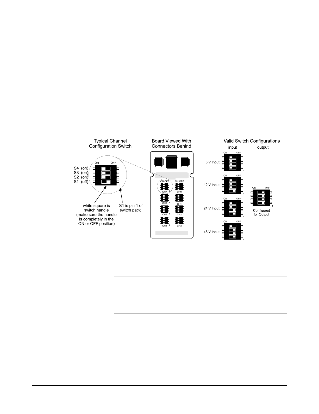
Setting Configuration Switches
Each channel has a four-switch package that configure its input threshold
voltage level and I/O direction.
Locating switches Figure 1 shows the location of each chann el's confi guration switch pac kage.
Figure 1 Locating and Setting Threshold Switches
Important! Make certai n that you slide the swit ch handles complet ely to the ON or OFF
position! Verify switch se ttin gs with th e
An invalid switch sett ing will cause the r elated channel to be have as an input
with unknown threshold level.
4 VT1536A Isolated Digital Input/Output SCP
INP:THReshold:LEVel? command.
Page 5

Configuring for Input Refer again to Figure 1 for the four valid input threshold, switch
configurations. Table 1 shows the "input zero" and "input one" levels for the
nominal threshold settings.
Table 1 Input Threshold Voltage Levels
Nominal
Threshold Level
5 2.1 1.4
12 7 2
24 13 3
48 25 5
Input One
VDC Minimum
Input Zero
VDC Maximum
Configuring for Output By turning all four of its threshold-setting switches OFF, a channel is
configured as an output channel.
Installation
After the switches have been conf igured, the installat io n for th is Pl ug- on is
common to several other s and is covered in Ch apt er 1 o f your VXI Module
User's Manual.
Connecting To The Terminal Module
T o get sta rted on field wiring to the VT1536A SCP you'll nee d to know that
input-configured cha nnels ARE POLARIZED. That is the H ter mina l must
be driven positive rela tive to the L terminal. Output-con figured channels are
not polarized. For more i nform ati on see
“Input and Output Character isti cs ”
on page 7.
The SCP connections for the Terminal Modules are shown on the
self-adhesive labels that come with the SCP. Use these to label terminal
definitions on your t erminal module . The connections a re shown in
Figure 2.
VT1536A Isolated Digital Input/Output SCP 5
Page 6

Figure 2 VT1415A/19A/22A Terminal Module Connections
Recommended Signal Connections
Figure 3 shows the recommended method of wiring isolated digital I/O
channels, as well as the maximum voltage limitations for the VT1536A.
Figure 3 shows the shield s connected di rectly to the VT1415 A/19A ground.
This is to limit potential noise on the isolated digital wiring from affecting
low-level analog channel wiring within the Terminal Module.
Note The VT1536A is a true isolated SCP. There is no electrical connection
between each channel's Hi/Lo terminals and VT1415A/19A's chassis
ground. However the G (analog guard) terminals are connected through
kOhm resistors to chassis ground within the VT1415A/19A. These
10
terminals are NOT isolated.
6 VT1536A Isolated Digital Input/Output SCP
Page 7

Figure 3 Recommended Connections and Voltage Limits
Input and Output Characteristics
This section describes the electrical characteristics of the SCP's input and
output sections, as wel l as the operation of the i nput debounce timers.
4 shows a simplified schematic of one VT1536A channel.
Input Characteris tics The input section drives an opt o-isolator through a res istor threshol d setting
network. Your system must provide at least 1 mA of current to drive the
opto-isolator. The threshold setting network controls this drive current for
various input voltages ranging from 5 to 48 Volts (see
Your input voltage must be polarized positive to the Hnn terminal, and
negative to the Lnn terminal.
Output Characteristics The opto-isolated output provides a Solid-State relay and relay protection
voltage clamping diode. The soli d sta te rel ay is non -po lar i zed. The voltage
clamping diode limits voltage at the relay output to 80 V
conduct at about 60 V
off-resistance is at least 10
). The SS relay's on-resistance is 10 Ω,
PEAK
10
Ω. The relay's turn-on time is 3 millisec onds.
Table 1 on page 5).
(begins to
PEAK
Figure
VT1536A Isolated Digital Input/Output SCP 7
Page 8

Figure 4 The VT1536A Input and Output Sections
113
Output Voltage Clamp The output section incorporates a "crowbar" protection type voltage
clamping diode. In normal operation with the relay voltage at or below
Volts peak, the diode has virtually no effect (other than about
56
nanoamperes of leakage cur rent). At 60 Volts, the diode starts to conduc t
10
to limit further voltage excursions. In this region, the diode effectively
clamps momentary voltage spikes from inductive loads. If an overvoltage
condition occurs that drives a voltage surge in the diode to 80 Volts, the
diode will latch-on, clamping the voltage to a few volts. This latched-on
condition will continue unti l the curr ent surge through the diode is reduced
to less than 150 mA, whereupon the diode returns to its off state.
Debounce Function Setting the appropriate debounce period ensures that the VT1415A/19A
algorithm reads only the most current VALID digital input state as latched
into the SCP channel . By " val id" we mean that the signal has not made any
0-to-1 or 1-to-0 transitions for the duration of the debounce period (the
signal has settled). If the alg orithm reads a channel that has not yet settled,
it will receive the previously latched valid state (no change).
Debounce is controlled using VT1415A/19A SCPI commands. When the
debounce feature is enable d, inputs are tested f or debounc e, and vali d state s
debounce periods. This debounce-and-latch rate is
are latched every
⁄
8 VT1536A Isolated Digital Input/Output SCP
Page 9

completely asynchron ous with th e VT1415A/19A al gorit hm executi on rate
as set by the Trigge r Timer (
TRIG:TIMER command). Long debounce
periods combined wi th fast T rigger T imer set tings would have t he algorithm
executing several times for each input debounce-and-latch period.
Conversely, short debounce periods and slow Trigger Timer rates would
allow multiple debounce-and-latches per algorithm execution.
Debounce Example Figure 5 demonst rates the use of debounce. Her e we show a system that uses
a digital line to sense a switch an operator would throw to signal the
algorithm to shut do wn a process. The digi tal line runs t hrough an el ectrica l
environment that could cause a false shut-down signal when a large motor
starts. The motor sta rt period is at most 0.5 second s. The algorit hm executes
every 100 ms so without debounce it could sense this electrical noise as a
false shut-down signal. If we set the de boun ce per io d to 1.228 seconds, the
VT1536A will ignore the motor start-up noise and will only latch signal
states that last as long or longer than the debounce period.
Figure 5 Example Using Debounce Feature
Data Latency With the debounce feature on, the data latency (the time from valid signal
transition to acquisi ti on by the al gor it hm is up to 1.333 times the debounce
period plus one VT1415A/19A trigger repetition period
TRIG:TIM:PERIOD).
(
With the debounce feature off (INPut:DEBounce 0,(@<ch_list>), the
latency is only the algorithm repetition rate.
VT1536A Isolated Digital Input/Output SCP 9
Page 10

Programming With SCPI Commands
The SCPI commands shown here quer y the SCP's identificati on st ri ng, and
perform VT1536A channel configuration. The VT1415A/19A doesn't
provide SCPI commands to read an input channel or control an output
channel. Read and write operations are performed by the VT1415A/19A's
Algorithm language. See the following section for a digital input/output
example.
*RST & Power-up
Conditions
Checking the ID
of the SCP
The default configuration of the VT1536A at power-up or after a *RST
command is:
• Channel I/O direction is as set by the threshold/direction switches
(
See “Setting Configuration Switch es” on page 4.).
• Input and output channel polarity will be NORMal. This means:
-- For inputs; when the input opto isolator is being driven (is "on"), an
algorithm will read a logic 1. When the opto is off, the algorithm
reads a zero.
-- For outputs; when an alg orith m writes a 1, th e output rel ay will turn
on ("close" ). Writing a zero will turn the relay off.
Remember, polarity NORMal means "1 = ON".
•Output configured channels will have their relays turned off ("open").
To verify the SCP type(s) installed on your VXI module, use the
SYSTem:CTYPE? (@<channel>) command.
•The channel parameter specifies a single channel in the channel range
covered by the SCP of interest. The first channel number for each of
the eight SCP positions are; 0,8,16,24,32,40,48, and 56.
The value returned for the VT1536A SCP is:
HEWLETT-PACKARD,E1536A Isolated Digital I/O SCP,0,0
To determine the type of SCP installed on channels 0 through 7 send
SYST:CTYPE? (@100)
enter statement here
Determining Input
Threshold Level and
I/O Direction
The input threshold level and I/O direction is set (for each individual
channel) by hardware switche s (
page 4.). To determine how a channel is currently configured, use the
command:
INPut:THReshold:LEVel? (@<channel>)
•Channel must specify a single channel
10 VT1536A Isolated Digital Input/Output SCP
query SCP type @ ch 0
enter response string
See “Setting Configuration Switches” on
Page 11

•INP:THR:LEV? returns a numeric value which is one of 5 , 12 , 24, 48 or
0 (zero) where zero means that the channel is configured as an output
and non-zero values indicate the input threshold in volts.
Note If an invali d switch combination is set, INP:THR:LEV? will NOT return a
value and will generate the error 3105 "Invalid SCP switch setting". This
error will also be generated w hen
with this error will behave as i nput channe ls with unk nown thresh old lev els.
To query the threshold level on the second channel at SCP position 2 send:
*RST is executed. Channels associated
Configuring Input
Channel Polarity
INP:THR:LEV? (@117)
enter statement here
To configure input channel polarity use the command:
INPut:POLarity INVerted | NORMal,
T o config ure the first 2 channels on an VT153 6A in SCP position 4 to input
Normal polarity (opt o on=logical 1) and its next 2 c hannels to input inverted
polarity (opto off=logical 1)send:
INP:POL NORM,(@132,133)
INP:POL INV,(@134,135)
There is also the query form; INPut:POLarity? (@<channel>), where
<channel> must specify a single channel.
(@<ch_list>)
query 2nd chan on SCP pos. 2
returns 0 | 5 | 12 | 24 | 48
NORM is *RST default
INP:POL? returns NORM | INV.
Note The INPut:POL command will generate the error 3107, "Channel data
direction confl icts with command " if any channe l in <ch_list> is configured
as an output.
Setting Debounce Time For a description of the debounce function See “Debounce Function” on
page 8. The VT1536A has two debounce timers. One for the lower four
channels, and one for the upper four channels. To set the debounce timers
use the command:
INPut:DEBounce:TIME <time>,(@<ch_list>)
•<time> can be one of 16 possible numeric values or MIN and MAX:
Note Because the clock that generates the debounce period is asynchronous to
your input signal, there is a region of uncertainty relative to the nominal
debounce period selected. This is reflected in the “Minimum” and
“Maximum” debounce period columns in
VT1536A Isolated Digital Input/Output SCP 11
Table 2.
Page 12

Choose a value from the “Minimum Period” column in Table 2 that is
longer than your input signal’s undesired transition period when you
want to exclude these short term input signal transitions.
Choose a value fro m the “M ax im um Period” column in Table 2 that is
shorter than your input signal’s expected transition period when you
want to be certain to include these desired input signal transitions.
The values to send to the VT1536A are in the “Nominal” column in
Table 2 below.
Table 2 Nominal Debounce Period and Uncertainties
Minimum Period Nominal Value Maximum Period
debounce off 0 debounce off
0.08 ms 0.15 ms 0.18 ms
0.20 ms 0.30 ms 0.35 ms
0.45 ms 0.60 ms 0.65 ms
0.95 ms 1.20 ms 1.30 ms
1.90 ms 2.40 ms 2.50 ms
4.10 ms 4.80 ms 5.00 ms
8.20 ms 9.60 ms 9.85 ms
16.4 ms 19.2 ms 19.7 ms
32.8 ms 38.4 ms 39.4 ms
65.5 ms 76.6 ms 78.7 ms 131 ms 153.6 ms 158 ms 262 ms 307.2 ms 315 ms 525 ms 614.4 ms 630 ms
1.05 s 1.2288 s 1. 26 s
2.10 s 2.4576 s 2. 52 s
-- Sending 0 or MIN turns debounce off. Sending MAX selects 2.458
seconds.
-- If a value is sent t hat is slightly greater than one of these va lue s, t h e
next higher value (or
MAX) is selected. Values outside of th e range
0 - 2.4576 will generate the error -222, "Data out of range".
•<ch_list> must conta in al l 4 of the upper - ban k channels, or all 4 of th e
lower-bank channe ls, or all 8 ch annels for a gi ven SCP. This is because
the VT1536A has two debounce timers, one for its lower
and one for its upper 4 channels.
4 channels
12 VT1536A Isolated Digital Input/Output SCP
Page 13

Note The INP:DEB:TIME generate the error 3108, "E1536 debounce - each
referenced 4 Ch bank must co ntain at least one i nput". This error indicates
that you tried t o set a debounc e t ime for a bank of channe ls th at contai ns no
input configured channel.
To set the debounce period to 153.6 ms for the lower 4 channels on an
VT1536A in SCP position 0 send:
INP:DEB 0.1536,(@100:103)
To set the debo unce per i od t o 1.229 seconds for th e upp er 4 channels on an
VT1536A in SCP position 3 send:
INP:DEB 1.229,(@128:131)
There is also the query form;
INPut:DEBounce:TIME? (@<channel>)
where <channel> must specify a single channel. INP:DEB:TIME? returns
the currently set debounce period.
Configuring Output
Channel Polarity
Notes 1. The OUTPut:POL command will generate the error 3107, "Channel
To configure output channel polarity use the command:
OUTPut:POLarity INVerted | NORMal,(@<ch_list>)
T o c onfigur e the fif th and sixt h channe ls on an VT1536A in SCP posi tion 4
to output normal polarity (logical 1=relay on) and its next 2 channels to
output inverted polarity (logical 1=relay off) send:
OUTP:POL NORM,(@136,137)
OUTP:POL INV,(@138,139)
NORM is *RST default
There is also the query form; OUTPut:POLarity? (@<channel>), where
<channel> must specify a s ingle channel.
OUTP:POL? returns "NORM" or
"INV".
data direction conflicts with command" if a ny channel in <ch_list> is
configured as an input.
2. An output channel's SS relay will not change from the *RST state
(open) regardless of its
POLarity setting, until an algorithm writes a
value to that channel.
VT1536A Isolated Digital Input/Output SCP 13
Page 14

Programming with the VT1415A/19A Algorithm Language
The following example shows the command sequence (platform/language
independent) to transfer the di gital s tates from the lower 4 channels (input s)
to the upper 4 channe ls (outputs). In other wor ds, t he state you input t o on e
of the lower 4 channels will drive the corresponding output channel. The
example assumes that the SCP is installed in SCP position 0
(covers
inputs, and the last four are configured as outputs (
Configuration Switches” on page 4.).
*RST reset module to default states
ALG:DEF 'ALG1','O104=I100; O105=I101; O106=I102; O107=I103;'defines the algorithm
INIT start algorithm (using default trig sys setup)
When the algorithm is run, digital states input to channels 0 through 3 will
be output on channels 4 through 7.
channels 0 through 7), the first four channels are configured as
See “Setting
*RST and *TST? (Important!)
The *RST/Power-up state and *TST? command reset the VT1415A/19A to
its default state. This will cause all output-configured channel solid-state
relays to "open" ( turn of f), disable debounce, and r estore channel polarity t o
normal. Keep this in mind when a pplying the VT1536A SCP to y our system
and design the "open" state as the safe state for your system.
Note *RST will report error 3105, "Invalid SCP switch setting" if one or more
configuration switches are set to invalid configurations.
14 VT1536A Isolated Digital Input/Output SCP
Page 15

Specifications
SCP Power Supply Requirements
+5 Vmax +24 Vtyp +24 Vmax -24 Vtype -24 Vmax
0.072 not used not used
Output Characteristics
(see also Figure 4)
Input Characteristics
(see also Figure 4)
Characteristic Specification
Maximum Continuous
Voltage
Peak Current Load 200 mA
Relay On Resistance
Turn On/Off Time 3 ms
Clamping Voltage* 60 V
* See “Output Voltage Clamp” on page 8.
Characteristic Specification
Maximum Continuous
Voltage
Maximum Input Zero See Table 1 on page 5
Minimum Input One See Table 1 on page 5
Input Debounce Ti me 150 µs - 2.4 s. See Table 2 on page 12
56 VDC (39 V
10 Ω
56 VDC (39 V
RMS
RMS
)
)
VT1536A Isolated Digital Input/Output SCP 15
Page 16

Notes:
16 VT1536A Isolated Digital Input/Output SCP
 Loading...