

Page 1

Artisan Technology Group is your source for quality
new and certied-used/pre-owned equipment
• FAST SHIPPING AND
DELIVERY
• TENS OF THOUSANDS OF
IN-STOCK ITEMS
• EQUIPMENT DEMOS
• HUNDREDS OF
MANUFACTURERS
SUPPORTED
• LEASING/MONTHLY
RENTALS
• ITAR CERTIFIED
SECURE ASSET SOLUTIONS
SERVICE CENTER REPAIRS
Experienced engineers and technicians on staff
at our full-service, in-house repair center
WE BUY USED EQUIPMENT
Sell your excess, underutilized, and idle used equipment
We also offer credit for buy-backs and trade-ins
www.artisantg.com/WeBuyEquipment
REMOTE INSPECTION
Remotely inspect equipment before purchasing with
our interactive website at www.instraview.com
LOOKING FOR MORE INFORMATION?
Visit us on the web at www.artisantg.com for more
information on price quotations, drivers, technical
specications, manuals, and documentation
Contact us: (888) 88-SOURCE | sales@artisantg.com | www.artisantg.com
SM
View
Instra
Page 2

bus
VT1419A
Plus
Multifunction
Measurement and Control Module
User’s Manual
APPLICABILITY
This manual edition is intended for use with the following instrument drivers:
·
Downloaded driver revision A.01.02 or later for Command Modules
·
C-SCPI driver revision D.01.02 or later
Call your local VXI Technology Sales Office for information on other drivers.
Artisan Technology Group - Quality Instrumentation ... Guaranteed | (888) 88-SOURCE | www.artisantg.com
Copyright © VXI Technology, Inc., 2005
P/N: 82-0075-000
Printed: August 15, 2005
Printed in U.S.A.
Page 3

Certification
VXI Technology,Inc., certifies that this product metits published specifications at the timeof shipment fromthe factory. VXI Technology
further certifies that its calibration measurements are traceable to the United States National Institute of Standards and Technology
(formerly National Bureau of Standards), to the extent allowed by that organization’s calibration facility and to the calibration facilities
of other International Standards Organization members.
Warranty
This VXI Technology product is warranted against defects in materials and workmanship for a period of three years from date of
shipment. Duration and conditions of warranty for this product may be superseded whenthe product is integratedinto (becomes a partof)
other VXITechnology products. During thewarranty period, VXI Technology, will,at its option,either repair orreplace products which
prove to be defective.
For warranty service or repair, this product must be returned to a service facility designated by VXI Technology. Buyer shall prepay
shipping charges to VXI Technology and VXI Technology shall pay shipping charges to return the product to Buyer. However, Buyer
shall pay all shipping charges, duties, and taxes for products returned to VXI Technology from another country.
VXI Technology warrants that its software and firmware designated by VXI Technology for use with a product will execute its
programming instructions whenproperly installed onthat product. VXI Technology does not warrant that the operation of theproduct or
software or firmware will be uninterrupted or error free.
Limitation Of Warranty
The foregoing warranty shall not apply to defects resulting from improper or inadequate maintenance by Buyer, Buyer-supplied products
or interfacing, unauthorized modification or misuse, operation outside of the environmental specifications for the product or improper
site preparation or maintenance.
The design andimplementation of any circuit onthis product is the soleresponsibility of the Buyer. VXI Technology doesnot warrant the
Buyer’s circuitry or malfunctions of VXI Technology products that result from the Buyer’s circuitry. In addition, VXI Technology does
not warrant any damage that occurs as a result of the Buyer’s circuit or any defects that result from Buyer-supplied products.
NO OTHER WARRANTY IS EXPRESSED OR IMPLIED. VXI TECHNOLOGY SPECIFICALLY DISCLAIMS THE IMPLIED
WARRANTIES OF MERCHANTABILITY AND FITNESS FOR A PARTICULAR PURPOSE.
Exclusive Remedies
THE REMEDIES PROVIDED HEREINAREBUYER’SSOLE AND EXCLUSIVE REMEDIES. VXI TECHNOLOGY SHALL NOT
BE LIABLE FOR ANY DIRECT, INDIRECT, SPECIAL, INCIDENTAL OR CONSEQUENTIAL DAMAGES, WHETHER BASED
ON CONTRACT, TORT, OR ANY OTHER LEGAL THEORY.
Notice
The information contained in this document is subject to change without notice. VXI TECHNOLOGY MAKES NO WARRANTY OF
ANY KIND WITH REGARD TO THIS MATERIAL, INCLUDING, BUT NOT LIMITED TO, THE IMPLIED WARRANTIES OF
MERCHANTABILITY AND FITNESS FOR A PARTICULAR PURPOSE. VXI Technology shall not be liable for errors contained
herein or for incidental or consequential damages in connection with the furnishing, performance, or use of this material. This document
contains proprietary information which is protected by copyright. All rights are reserved. No part ofthis document may be photocopied,
reproduced, or translated to another language without the prior written consent of VXI Technology. VXI Technology assumes no
responsibility for the use or reliability of its software on equipment that is not furnished by VXI Technology.
Restricted Rights Legend
U.S. Government Restricted Rights. The Software and Documentation have been developed entirely at private expense. They are
delivered and licensedas “commercial computer software” asdefined in DFARS 252.227- 7013(Oct1988), DFARS 252.211-7015 (May
1991) or DFARS 252.227-7014 (Jun 1995), as a “commercial item” as defined in FAR 2.101(a) or as “Restricted computer software” as
defined in FAR 52.227-19 (Jun 1987)(or any equivalent agency regulation or contract clause), whichever is applicable. You have only
those rights provided for such Software and Documentation by the applicable FAR or DFARS clause or the VXI Technology standard
software agreement for the product involved.
2
Artisan Technology Group - Quality Instrumentation ... Guaranteed | (888) 88-SOURCE | www.artisantg.com
Page 4

Safety Symbols
Instruction manual symbol affixed to
product. Indicates that the user must refer
Alternating current (ac).
to the manual for specific WARNING or
CAUTION information to avoid personal
injury or damage to the product.
Direct current (dc).
Indicates hazardous voltages.
Indicates the field wiring terminal that must
be connected to earth ground before
operating the equipment—protects against
electrical shock in case of fault.
or
Frame or chassis ground
terminal—typically connects to the
WARNING
CAUTION
equipment’s metal frame.
Calls attention to a procedure, practice or
condition that could cause bodily injury or
death.
Calls attention to a procedure, practice, or
condition that couldpossibly cause damage to
equipment or permanent loss of data.
Warnings
The following general safety precautions must be observed during all phases of operation, service, and repair of this product.
Failure to comply with these precautions or with specific warnings elsewhere in this manual violates safety standards of design,
manufacture and intended use of the product. VXI Technology assumes no liability for the customer’s failure to comply with
these requirements.
Ground the equipment: For Safety Class 1 equipment (equipment having a protective earth terminal), an uninterruptible safety earth
ground must be provided from the mains power source to the product input wiring terminals or supplied power cable.
DO NOT operate the product in an explosive atmosphere or in the presence of flammable gases or fumes.
For continued protection against fire, replace the line fuse(s) only with fuse(s) of the same voltage and current rating and type.
DO NOT use repaired fuses or short-circuited fuse holders.
Keep away from live circuits: Operating personnel must not remove equipment covers or shields. Procedures involving the removal of
covers or shields are for use by service-trained personnel only. Under certain conditions, dangerous voltages may exist even with the
equipment switched off. To avoid dangerouselectrical shock, DO NOTperform procedures involving cover or shield removal unlessyou
are qualified to do so.
DO NOT operate damaged equipment: Whenever it is possible that the safety protection features built into this product have been
impaired, either through physical damage, excessive moisture or any other reason, REMOVE POWER and do not use the product until
safe operation can be verified by service-trained personnel. If necessary, return the product to a VXI Technology Sales and Service
Office for service and repair to ensure that safety features are maintained.
Note for European Customers
If this symbolappears on your product,itindicates that it was manufactured after August 13,2005.This markisplaced in accordance with EN
50419, Marking of electrical and electronic equipment in accordance with Article 11(2) of directive 2002/96/EC (WEEE). End-of-life
product can be returned to VTI by obtaining an RMA number.Feesforrecyclingwillapplyif not prohibited by national law. SCP cards for use
with the VT1415A have this mark placed on their packaging due to the densely populated nature of these cards.
Artisan Technology Group - Quality Instrumentation ... Guaranteed | (888) 88-SOURCE | www.artisantg.com
3
Page 5

4
Artisan Technology Group - Quality Instrumentation ... Guaranteed | (888) 88-SOURCE | www.artisantg.com
Page 6

Table of Contents
Warranty ................................................................. 2
Warnings ................................................................. 3
Safety Symbols ............................................................ 3
Note for European Customers .................................................3
Support Resources......................................................... 13
Chapter 1. Getting Started ....................................................... 15
About This Chapter ........................................................15
Configuring the VT1419A .................................................. 15
Setting the Logical Address Switch.......................................... 15
Installing SCPs ......................................................... 16
Disabling the Input Protect Feature (Optional) ................................. 21
Disabling Flash Memory Access (Optional) ...................................21
Instrument Drivers......................................................... 23
About Example Programs ................................................... 23
Verifying a Successful Configuration ..........................................23
Chapter 2. Field Wiring.......................................................... 25
About This Chapter ........................................................25
Planning the Wiring Layout ................................................. 25
SCP Positions and Channel Numbers ........................................ 25
SCP Types and Signal Paths ............................................... 25
Pairing Sense and Source SCPs for Resistance Measurements .....................27
Planning for Thermocouple Measurements....................................28
Faceplate Connector Pin-Signal Lists .......................................... 29
Optional Terminal Modules ................................................. 30
The SCPs and Terminal Module Connections.................................. 30
Option 11 Terminal Module Layout ......................................... 31
Option 12 Terminal Module Layout ......................................... 32
Reference Temperature Sensing with the VT1419A...............................33
Configuring the On-Board/Remote Reference Jumpers ............................34
Preferred Measurement Connections .......................................... 36
Wiring and Attaching the Terminal Module .....................................39
Attaching/Removing the VT1419A Terminal Module .............................41
Adding Components to the Option 12 Terminal Module ........................... 43
Option 11 Terminal Module Wiring Map .......................................44
Option 12 Terminal Module Wiring Map .......................................45
The Option A3F .......................................................... 46
Chapter 3. Programming the VT1419A Multifunction
About This Chapter ........................................................47
Overview of the VT1419A Multifunction
Multifunction
Operating Model .......................................................... 52
Executing The Programming Model ...........................................53
Power-On and *RST Default Settings ........................................ 53
Setting Up Analog Input and Output Channels ................................... 56
Configuring Programmable Analog SCP Parameters ............................56
Contents 5
Artisan Technology Group - Quality Instrumentation ... Guaranteed | (888) 88-SOURCE | www.artisantg.com
Plus
.................................47
Plus
Plus
?........................................................ 48
....................................48
Page 7

Setting Filter Cutoff Frequency ............................................. 57
Linking Channels to EU Conversion ......................................... 58
Linking Output Channels to Functions ....................................... 66
Setting Up Digital Input and Output Channels ................................... 66
Setting Up Digital Inputs .................................................. 66
Setting Up Digital Outputs ................................................ 67
Performing Channel Calibration (Important!)....................................71
Defining C Language Algorithms ............................................ 73
Global Variable Definition ................................................ 73
Algorithm Definition ..................................................... 74
Pre-Setting Algorithm Variables ............................................74
Defining Data Storage ...................................................... 75
Specifying the Data Format ................................................ 75
Selecting the FIFO Mode.................................................. 76
Setting up the Trigger System ................................................ 77
Arm and Trigger Sources ................................................. 77
Programming the Trigger Timer ............................................ 79
Setting the Trigger Counter ................................................79
Outputting Trigger Signals ................................................ 79
Initiating/Running Algorithms ............................................... 80
Starting Algorithms ...................................................... 80
The Operating Sequence .................................................. 81
Retrieving Algorithm Data .................................................. 81
Modifying Running Algorithm Variables .......................................85
Updating the Algorithm Variables and Coefficients .............................85
Enabling and Disabling Algorithms ......................................... 85
Setting Algorithm Execution Frequency ......................................86
Example Command Sequence................................................ 86
Using the Status System .................................................... 88
Enabling Events to be Reported in the Status Byte ..............................91
Reading the Status Byte................................................... 92
Clearing the Enable Registers .............................................. 93
The Status Byte Group’s Enable Register .....................................93
Reading Status Groups Directly ............................................ 93
VT1419A Background Operation .............................................94
Updating the Status System and VXIbus Interrupts ............................... 95
Creating and Loading Custom EU Conversion Tables .............................96
Compensating for System Offsets ............................................. 97
Special Considerations.................................................... 99
Detecting Open Transducers ................................................100
More On Auto Ranging.................................................... 101
Settling Characteristics .................................................... 101
Background ........................................................... 101
Checking for Problems .................................................. 102
Fixing the Problem ..................................................... 102
Chapter 4. The Algorithm Language and Environment ..............................105
About This Chapter .......................................................105
Overview of the Algorithm Language......................................... 106
Example Language Usage ................................................107
The Algorithm Execution Environment ....................................... 108
The Main Function
6 Contents
Artisan Technology Group - Quality Instrumentation ... Guaranteed | (888) 88-SOURCE | www.artisantg.com
..................................................... 108
Page 8

How User Algorithms Fit In .............................................. 108
Accessing the VT1419A’s Resources .........................................109
Accessing I/O Channels.................................................. 110
Defining and Accessing Global Variables....................................111
Determining First Execution (First_loop) .................................... 111
Initializing Variables .................................................... 112
Sending Data to the CVT and FIFO ........................................ 112
Setting a VXIbus Interrupt ............................................... 113
Calling User Defined Functions ........................................... 114
Operating Sequence....................................................... 114
Overall Sequence....................................................... 114
Algorithm Execution Order ............................................... 116
Defining Algorithms (ALG:DEF) ............................................ 116
ALG:DEFINE in the Programming Sequence................................. 116
ALG:DEFINE’s Two Data Formats ........................................ 117
Changing an Algorithm While It Is Running ................................. 118
A Very Simple First Algorithm..............................................120
Writing the Algorithm ...................................................120
Running the Algorithm .................................................. 120
Non-Control Algorithms ................................................... 121
Data Acquisition Algorithm .............................................. 121
Process Monitoring Algorithm ............................................ 121
Algorithm Language Reference ............................................. 122
Standard Reserved Keywords ............................................. 122
Special VT1419A Reserved Keywords ...................................... 122
Identifiers............................................................. 122
Special Identifiers for Channels............................................ 123
Operators ............................................................. 123
Intrinsic Functions and Statements ......................................... 124
Program Flow Control ................................................... 124
Data Types............................................................ 125
Data Structures ........................................................ 126
Using Type Float in Integer Situations ...................................... 127
Language Syntax Summary................................................. 129
Program Structure and Syntax...............................................133
Declaring Variables ..................................................... 133
Assigning Values....................................................... 133
The Operations Symbols ................................................. 134
Conditional Execution ................................................... 134
Comment Lines ........................................................ 136
Overall Program Structure................................................ 137
About This Chapter .......................................................139
Wiring Connections and File Locations for the Examples ......................... 143
Example File Location................................................... 143
Installing Example Files ................................................. 143
Virtual Front Panel Program ................................................ 144
Calibration.............................................................. 147
Function Test............................................................ 148
Programming Model Example............................................... 149
Error Checking .......................................................... 152
Configuration Display
..................................................... 153
Engineering Unit Conversion ............................................... 154
Contents 7
Artisan Technology Group - Quality Instrumentation ... Guaranteed | (888) 88-SOURCE | www.artisantg.com
Page 9

Custom Function Generation................................................ 156
Custom EU/Function Example .............................................. 158
Curve Fitting and EU Generation ............................................ 160
Interrupt Handling ........................................................ 161
Simple Data Logger Example ............................................... 163
Modification of Variables and Arrays ......................................... 166
Algorithm Modification.................................................... 168
Driver Download......................................................... 170
Firmware-Update Download ................................................ 171
Chapter 6. VT1419A Command Reference ......................................... 173
ABORt ................................................................ 185
ALGorithm ............................................................. 186
ALGorithm[:EXPLicit]:ARRay ........................................... 187
ALGorithm[:EXPLicit]:ARRay? .......................................... 188
ALGorithm[:EXPLicit]:DEFine ........................................... 188
ALGorithm[:EXPLicit]:SCALar ..........................................192
ALGorithm[:EXPLicit]:SCALar? ......................................... 193
ALGorithm[:EXPLicit]:SCAN:RATio ...................................... 193
ALGorithm[:EXPLicit]:SCAN:RATio? ..................................... 194
ALGorithm[:EXPLicit]:SIZe? ............................................ 194
ALGorithm[:EXPLicit][:STATe] .......................................... 195
ALGorithm[:EXPLicit][:STATe]? ......................................... 196
ALGorithm[:EXPLicit]:TIME? ........................................... 196
ALGorithm:FUNCtion:DEFine ........................................... 197
ALGorithm:OUTPut:DELay .............................................198
ALGorithm:OUTPut:DELay? ............................................ 199
ALGorithm:UPDate[:IMMediate] ......................................... 199
ALGorithm:UPDate:CHANnel ............................................200
ALGorithm:UPDate:WINDow ............................................ 202
ALGOrithm:UPDate:WINDow? .......................................... 203
ARM.................................................................. 204
ARM[:IMMediate] ..................................................... 205
ARM:SOURce ........................................................ 205
ARM:SOURce? ........................................................ 206
CALibration ............................................................ 207
CALibration:CONFigure:RESistance ...................................... 208
CALibration:CONFigure:VOLTage ........................................ 209
CALibration:SETup..................................................... 210
CALibration:SETup?....................................................210
CALibration:STORe .................................................... 211
CALibration:TARE .................................................... 212
CALibration:TARE:RESet ............................................... 214
CALibration:TARE? .................................................... 214
CALibration:VALue:RESistance ......................................... 214
CALibration:VALue:VOLTage ........................................... 215
CALibration:ZERO? .................................................... 216
DIAGnostic ............................................................. 218
DIAGnostic:CALibration:SETup[:MODE]................................... 219
DIAGnostic:CALibration:SETup[:MODE]?..................................219
DIAGnostic:CALibration:TARE[:OTDetect]:MODE ..........................220
DIAGnostic:CALibration:TARE[:OTDetect]:MODE?.......................... 220
8 Contents
Artisan Technology Group - Quality Instrumentation ... Guaranteed | (888) 88-SOURCE | www.artisantg.com
Page 10

DIAGnostic:CHECksum? ................................................ 221
DIAGnostic:CUSTom:LINear............................................. 221
DIAGnostic:CUSTom:PIECewise.......................................... 222
DIAGnostic:CUSTom:REFerence:TEMPerature ..............................222
DIAGnostic:IEEE ...................................................... 223
DIAGnostic:IEEE? ..................................................... 223
DIAGnostic:INTerrupt[:LINe] ............................................ 223
DIAGnostic:INTerrupt[:LINe]? ........................................... 224
DIAGnostic:OTDetect[:STATe] ...........................................224
DIAGnostic:OTDetect[:STATe]? .......................................... 225
DIAGnostic:QUERy:SCPREAD? ..........................................225
DIAGnostic:VERSion? .................................................. 226
FETCh? ................................................................ 227
FORMat................................................................ 229
FORMat[:DATA] ...................................................... 229
FORMat[:DATA]? ..................................................... 230
INITiate ................................................................ 232
INITiate[:IMMediate] ................................................... 232
INPut ................................................................. 233
INPut:DEBounce:TIME ................................................. 233
INPut:FILTer[:LPASs]:FREQuency ........................................ 234
INPut:FILTer[:LPASs]:FREQuency? .......................................235
INPut:FILTer[:LPASs][:STATe] .......................................... 236
INPut:FILTer[:LPASs][:STATe]?.......................................... 236
INPut:GAIN .......................................................... 237
INPut:GAIN? ......................................................... 237
INPut:LOW ........................................................... 238
INPut:LOW? .......................................................... 238
INPut:POLarity ........................................................ 239
INPut:POLarity? ....................................................... 239
INPut:THReshold:LEVel?................................................ 239
MEMory ............................................................... 241
MEMory:VME:ADDRess ................................................ 242
MEMory:VME:ADDRess? ...............................................242
MEMory:VME:SIZE....................................................242
MEMory:VME:SIZE? ................................................... 243
MEMory:VME:STATe .................................................. 243
MEMory:VME:STATe? ................................................. 244
OUTPut ................................................................ 245
OUTPut:CURRent:AMPLitude............................................ 245
OUTPut:CURRent:AMPLitude? ........................................... 246
OUTPut:CURRent[:STATe] ..............................................247
OUTPut:CURRent[:STATe]? ............................................. 247
OUTPut:POLarity ...................................................... 248
OUTPut:POLarity? ..................................................... 248
OUTPut:SHUNt ....................................................... 248
OUTPut:SHUNt? ...................................................... 249
OUTPut:TTLTrg:SOURce ............................................... 249
OUTPut:TTLTrg:SOURce? .............................................. 250
OUTPut:TTLTrg<n>[:STATe] ............................................ 250
OUTPut:TTLTrg<n>[:STATe]?
........................................... 251
OUTPut:TYPE......................................................... 251
Contents 9
Artisan Technology Group - Quality Instrumentation ... Guaranteed | (888) 88-SOURCE | www.artisantg.com
Page 11

OUTPut:TYPE?........................................................252
OUTPut:VOLTage:AMPLitude ........................................... 252
OUTPut:VOLTage:AMPLitude? .......................................... 252
ROUTe ................................................................ 254
ROUTe:SEQuence:DEFine? ............................................. 254
ROUTe:SEQuence:POINts? .............................................. 255
SAMPle ................................................................ 256
SAMPle:TIMer ........................................................ 256
SAMPle:TIMer? ....................................................... 256
[SENSe]................................................................ 258
[SENSe:]CHANnel:SETTling.............................................259
[SENSe:]CHANnel:SETTling? ............................................ 260
[SENSe:]DATA:CVTable? .............................................. 260
[SENSe:]DATA:CVTable:RESet .......................................... 261
[SENSe:]DATA:FIFO[:ALL]? ............................................ 261
[SENSe:]DATA:FIFO:COUNt? ........................................... 262
[SENSe:]DATA:FIFO:COUNt:HALF? .....................................263
[SENSe:]DATA:FIFO:HALF? ............................................ 263
[SENSe:]DATA:FIFO:MODE ............................................ 264
[SENSe:]DATA:FIFO:MODE? ........................................... 264
[SENSe:]DATA:FIFO:PART? ............................................ 265
[SENSe:]DATA:FIFO:RESet ............................................. 265
[SENSe:]FREQuency:APERture........................................... 266
[SENSe:]FREQuency:APERture? .......................................... 267
[SENSe:]FUNCtion:CONDition ...........................................267
[SENSe:]FUNCtion:CUSTom............................................. 268
[SENSe:]FUNCtion:CUSTom:REFerence ................................... 269
[SENSe:]FUNCtion:CUSTom:TCouple ..................................... 270
[SENSe:]FUNCtion:FREQuency .......................................... 271
[SENSe:]FUNCtion:RESistance ........................................... 271
[SENSe:]FUNCtion:STRain:FBENding .....................................272
[SENSe:]FUNCtion:TEMPerature ......................................... 274
[SENSe:]FUNCtion:TOTalize............................................. 275
[SENSe:]FUNCtion:VOLTage[:DC] ....................................... 276
[SENSe:]REFerence .................................................... 277
[SENSe:]REFerence:CHANnels .......................................... 278
[SENSe:]REFerence:TEMPerature ........................................ 279
[SENSe:]STRain:EXCitation.............................................. 279
[SENSe:]STRain:EXCitation?............................................. 280
[SENSe:]STRain:GFACtor ............................................... 280
[SENSe:]STRain:GFACtor? .............................................. 280
[SENSe:]STRain:POISson ............................................... 281
[SENSe:]STRain:POISson?............................................... 281
[SENSe:]STRain:UNSTrained ............................................ 282
[SENSe:]STRain:UNSTrained? ........................................... 282
[SENSe:]TOTalize:RESet:MODE.......................................... 283
[SENSe:]TOTalize:RESet:MODE?......................................... 284
SOURce................................................................ 285
SOURce:FM[:STATe]................................................... 285
SOURce:FM:STATe? ................................................... 286
SOURce:FUNCtion[:SHAPe]:CONDition
...................................286
SOURce:FUNCtion[:SHAPe]:PULSe....................................... 287
10 Contents
Artisan Technology Group - Quality Instrumentation ... Guaranteed | (888) 88-SOURCE | www.artisantg.com
Page 12

SOURce:FUNCtion[:SHAPe]:SQUare ......................................287
SOURce:PULM[:STATe] ................................................287
SOURce:PULM:STATe? ................................................ 288
SOURce:PULSe:PERiod.................................................288
SOURce:PULSe:PERiod? ................................................ 289
SOURce:PULSe:WIDTh................................................. 289
SOURce:PULSe:WIDTh? ................................................ 289
STATus ................................................................ 291
STATus:OPERation:CONDition?..........................................293
STATus:OPERation:ENABle ............................................. 294
STATus:OPERation:ENABle? ............................................ 294
STATus:OPERation[:EVENt]? ............................................ 295
STATus:OPERation:NTRansition.......................................... 295
STATus:OPERation:NTRansition? .........................................296
STATus:OPERation:PTRansition ..........................................296
STATus:OPERation:PTRansition? ......................................... 297
STATus:PRESet ....................................................... 297
STATus:QUEStionable:CONDition? ....................................... 298
STATus:QUEStionable:ENABle .......................................... 299
STATus:QUEStionable:ENABle?.......................................... 299
STATus:QUEStionable[:EVENt]? ......................................... 299
STATus:QUEStionable:NTRansition ....................................... 300
STATus:QUEStionable:NTRansition? ...................................... 301
STATus:QUEStionable:PTRansition ....................................... 301
STATus:QUEStionable:PTRansition? ...................................... 302
SYSTem ............................................................... 303
SYSTem:CTYPe? ...................................................... 303
SYSTem:ERRor? ...................................................... 304
SYSTem:VERSion? .................................................... 304
TRIGger ............................................................... 305
TRIGger:COUNt ...................................................... 307
TRIGger:COUNt? ..................................................... 307
TRIGger[:IMMediate] .................................................. 308
TRIGger:SOURce ...................................................... 308
TRIGger:SOURce? .................................................... 309
TRIGger:TIMer[:PERiod] ............................................... 309
TRIGger:TIMer[:PERiod]? .............................................. 310
Common Command Reference ............................................. 311
*CAL? .............................................................. 311
*CLS ................................................................ 312
*DMC <name>,<cmd_data>.............................................312
*EMC ............................................................... 312
*EMC?............................................................... 312
*ESE <mask>......................................................... 312
*ESE? ............................................................... 313
*ESR? ............................................................... 313
*GMC? <name> ....................................................... 313
*IDN? ............................................................... 313
*LMC?............................................................... 313
*OPC ................................................................ 314
*OPC? ............................................................... 314
*PMC................................................................ 315
Contents 11
Artisan Technology Group - Quality Instrumentation ... Guaranteed | (888) 88-SOURCE | www.artisantg.com
Page 13

*RMC <name> ........................................................ 315
*RST ................................................................ 315
*SRE <mask>.........................................................316
*SRE? ............................................................... 316
*STB? ............................................................... 316
*TRG ................................................................ 316
*TST? ............................................................... 317
*WAI ................................................................ 320
Command Quick Reference ................................................ 321
Appendix A. Specifications ...................................................... 329
Appendix B. Error Messages .................................................... 359
Appendix C. Glossary .......................................................... 367
Appendix D. Wiring and Noise Reduction Methods .................................. 371
Separating Digital and Analog SCP Signals .................................... 371
Recommended Wiring and Noise Reduction Techniques ..........................372
Wiring Checklist ....................................................... 372
VT1419A Guard Connections ............................................. 373
Common Mode Voltage Limits ............................................ 373
When to Make Shield Connections .........................................373
Noise Due to Inadequate Card Grounding ..................................... 373
VT1419A Noise Rejection ................................................. 374
Normal Mode Noise (Enm) ...............................................374
Common Mode Noise (Ecm)..............................................374
Keeping Common Mode Noise out of the Amplifier ...........................374
Reducing Common Mode Rejection Using Tri-Filar Transformers ................375
Appendix E. Generating User Defined Functions .................................... 377
Introduction ............................................................. 377
Haversine Example ....................................................... 378
Limitations.............................................................. 380
Index ........................................................................ 381
12 Contents
Artisan Technology Group - Quality Instrumentation ... Guaranteed | (888) 88-SOURCE | www.artisantg.com
Page 14

Support Resources
Support resources for this product are available on the Internet and at VXI Technology
customer support centers.
VXI Technology
World Headquarters
VXI Technology, Inc.
2031 Main Street
Irvine, CA 92614-6509
Phone: (949) 955-1894
Fax: (949) 955-3041
VXI Technology
Cleveland Instrument Division
VXI Technology, Inc.
7525 Granger Road, Unit 7
Valley View, OH 44125
Phone: (216) 447-8950
Fax: (216) 447-8951
VXI Technology
Lake Stevens Instrument Division
VXI Technology, Inc.
1924 - 203 Bickford
Snohomish, WA 98290
Phone: (425) 212-2285
Fax: (425) 212-2289
Technical Support
Phone: (949) 955-1894
Fax: (949) 955-3041
E-mail: support@vxitech.com
Visit http://www.vxitech.com for worldwide support sites and service plan information.
Support 13
Artisan Technology Group - Quality Instrumentation ... Guaranteed | (888) 88-SOURCE | www.artisantg.com
Page 15

14 Contents
Artisan Technology Group - Quality Instrumentation ... Guaranteed | (888) 88-SOURCE | www.artisantg.com
Page 16

About This Chapter
This chapter will explain hardware configuration before installation in a VXIbus
mainframe. By attending to each of these configuration items, the VT1419A won’t
have to be removed from its mainframe later. Chapter contents include:
Configuring the VT1419A ............................page 15
·
Instrument Drivers .................................. page 23
·
About Example Programs .............................page 23
·
Verifying a Successful Configuration ....................page 23
·
Configuring the VT1419A
There are several aspects to configuring the module before installing it in a VXIbus
mainframe. They are:
Setting the Logical Address Switch .....................page 15
·
Installing Signal Conditioning Plug-ons ..................page 16
·
Disabling the Input Protect Feature ..................... page 21
·
Disabling Flash Memory Access .......................page 21
·
Chapter 1
Getting Started
NOTE Setting the VXIbus Interrupt Level: the VT1419A uses a default VXIbus interrupt
Setting the Logical
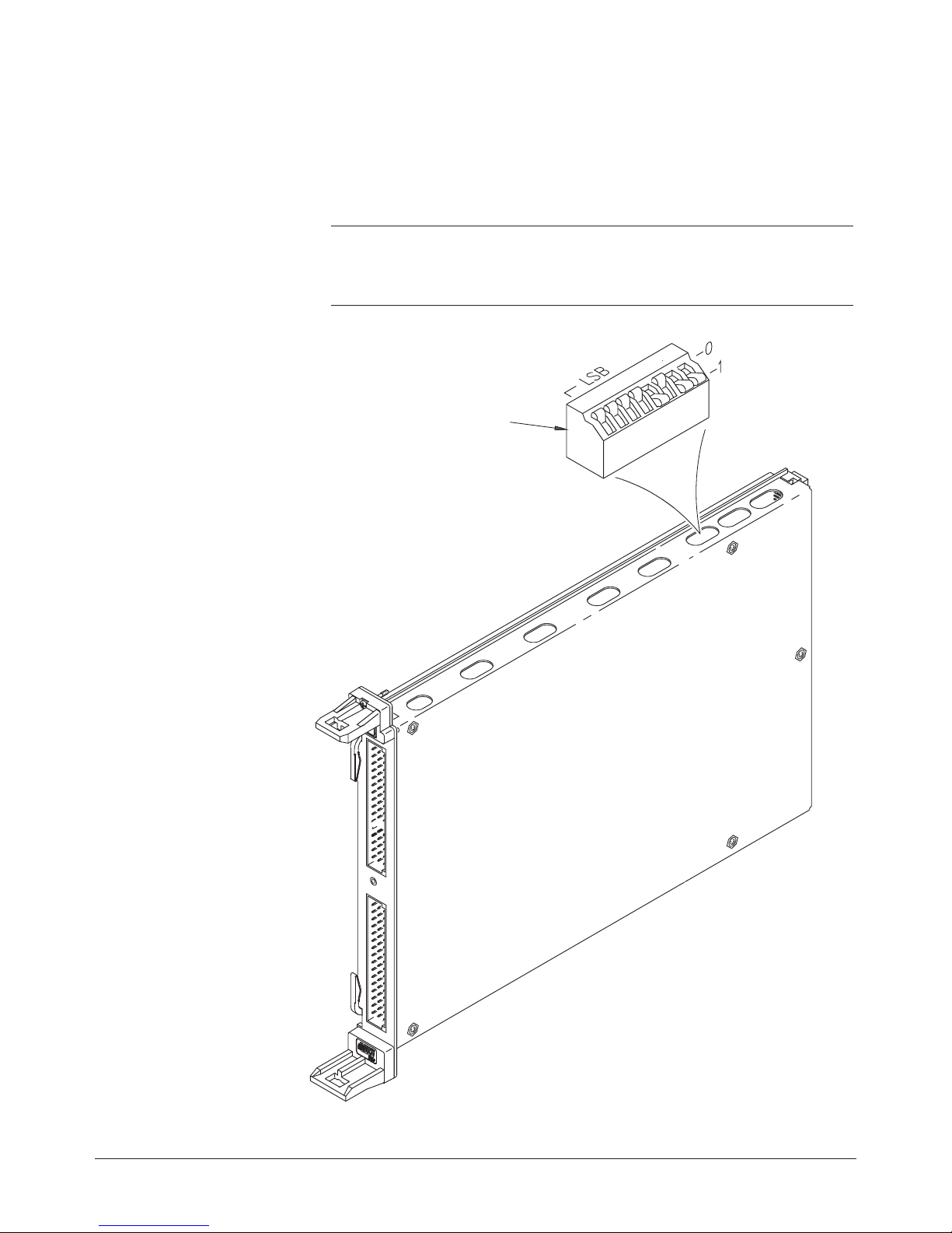
Address Switch
For most applications, only the Logical Address switch need be changed and the
SCPs installed in the mainframe prior to installation. The other settings can be
used as delivered.
Switch/Jumper Setting
Logical Address Switch
Input Protect Jumper
Flash Memory Protect Jumper
level of 1. The default setting is in effect at power-on and after a *RST command.
The interrupt level can be changed by executing the DIAGnostic:INTerrupt[:LINe]
command in the application program.
Follow the next figure and ignore any switch numbering printed on the Logical
Address switch. When installing more than one VT1419A in a single VXIbus
Mainframe, set each instrument to a different Logical Address.
208
Protected
PROG
Chapter 1 15
Artisan Technology Group - Quality Instrumentation ... Guaranteed | (888) 88-SOURCE | www.artisantg.com
Page 17
Getting Started
Configuring the VT1419A
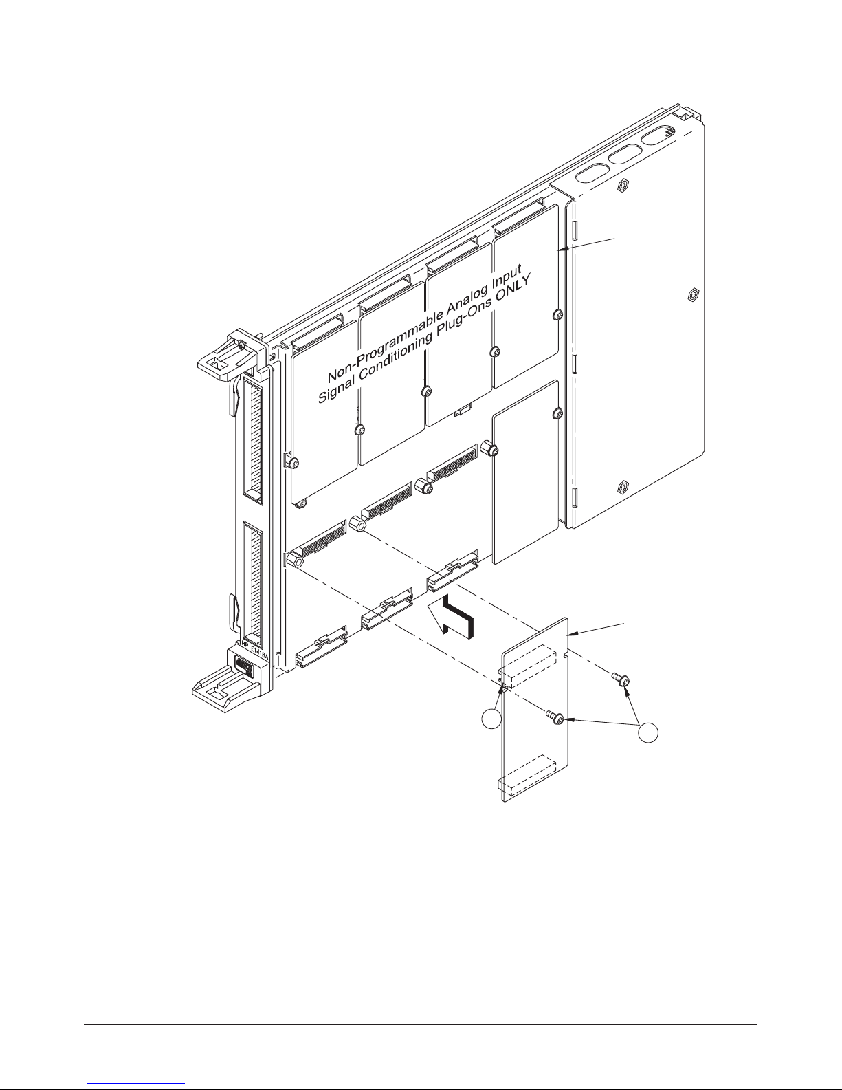
Installing SCPs The following illustrations show the steps used to install Signal Conditioning
Plug-Ons (SCPs). The VT1419A supports only non-programmable analog input
SCPs in positions 0 through 3. Any mix of SCP types can be installed in SCP
positions 4 through 7.
CAUTION Use approved Static Discharge Safe handling procedures anytime the covers are
removed from the VT1419A or are handling SCPs.
Setting Logical Address Switch – VT1419A
Default Switch Setting
LOGICAL ADDRESS = 208
16 Chapter 1
Artisan Technology Group - Quality Instrumentation ... Guaranteed | (888) 88-SOURCE | www.artisantg.com
Page 18

Note The only SCPs supported in SCP positions 0 through 3 are:
VT1501A VT1513A
VT1502A VT1514A
VT1508A VT1515A
VT1509A VT1516A
VT1512A VT1517A
1 InstallingSCPs: Removing theCover – VT1419A
Getting Started
Configuring the VT1419A
SCP
Remove the SCP
Retainer Screws
Chapter 1 17
Artisan Technology Group - Quality Instrumentation ... Guaranteed | (888) 88-SOURCE | www.artisantg.com
1
2
Remove 2 Screws;
Pull Cover Out
of the 3 slots
Page 19
Getting Started
Configuring the VT1419A
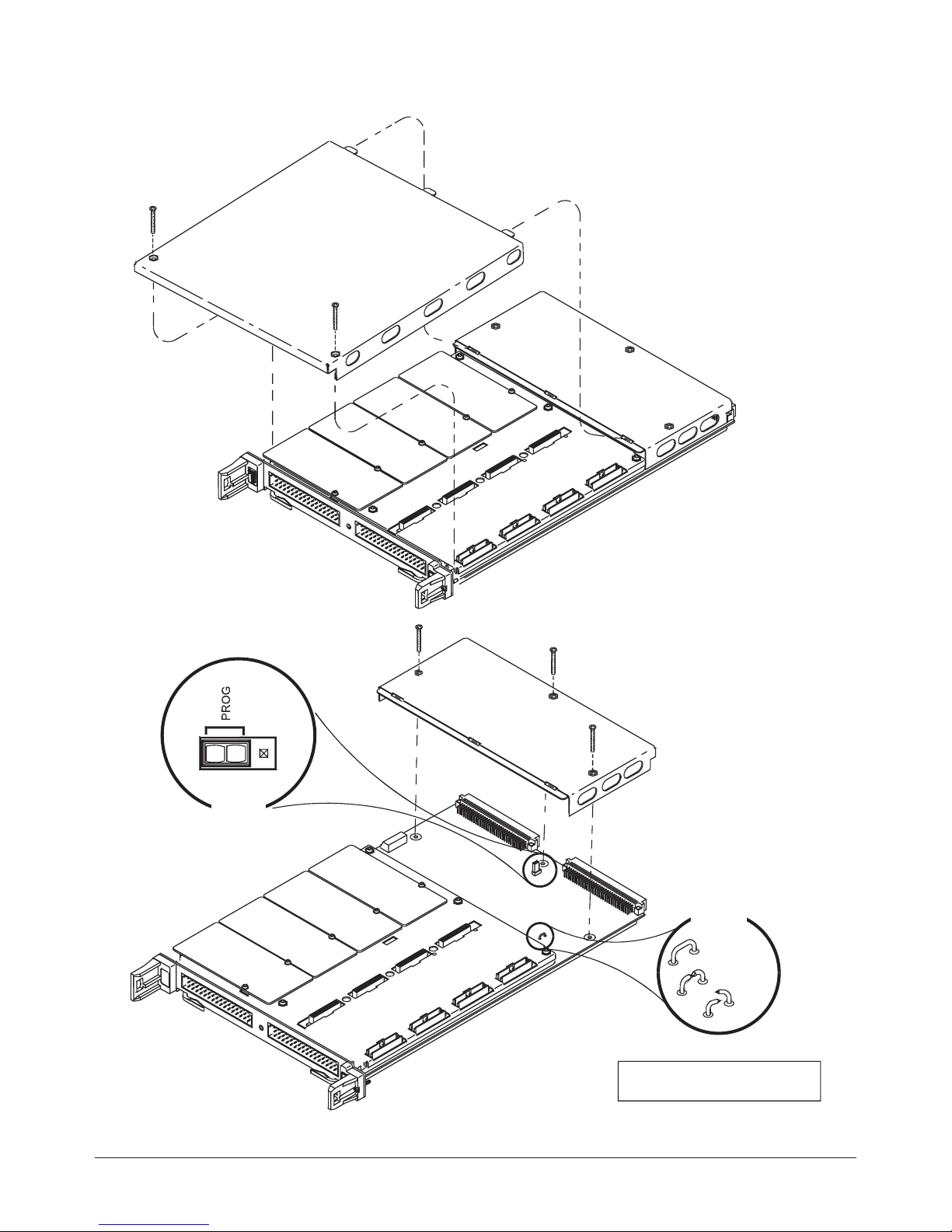
2 Installing SCPs – VT1419A
SCP
Align the SCP
Connectors with the
Module Connectors
and then Push In
SCP
1
2
Tighten the
SCP Retainer
Screws
18 Chapter 1
Artisan Technology Group - Quality Instrumentation ... Guaranteed | (888) 88-SOURCE | www.artisantg.com
Page 20
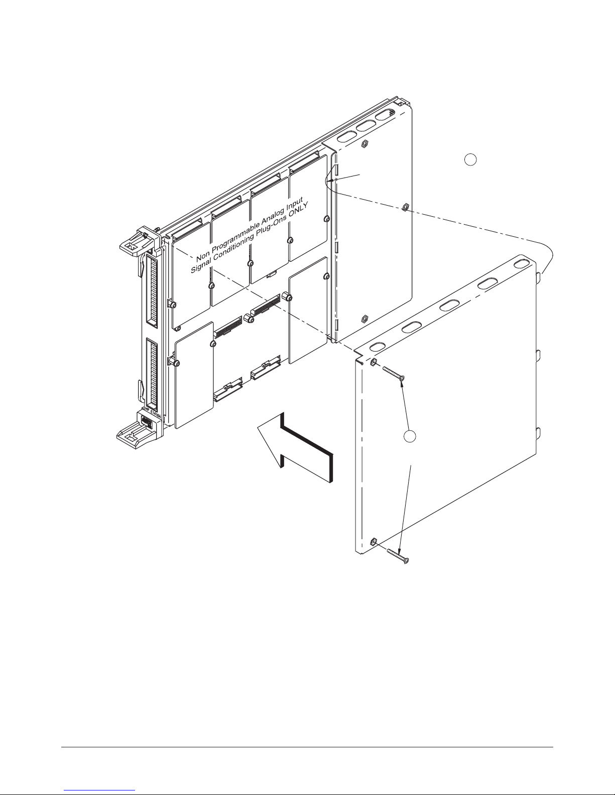
3 Installing SCPs: Reinstalling the Cover – VT1419A
SCP
Getting Started
Configuring the VT1419A
1
Line up the three tabs
with the three slots;
then push the cover
onto the module
2
Tighten two
screws
Chapter 1 19
Artisan Technology Group - Quality Instrumentation ... Guaranteed | (888) 88-SOURCE | www.artisantg.com
Page 21

Getting Started
Configuring the VT1419A
4 Installing SCPs: Labeling – VT1419A
1
Peel off label from
card and stick on
the appropriate
place on the cover
Terminal Module
(Connect to A/D
Module Later)
Terminal
Module
2
Peel off label from
card and stick on
the terminal module
to be connected
to the A/D Module
SCP
SCP
SCP
SCP
SCP
SCP
Stick-on labels
furnished with the SCP
(P/N: 43-0133-xxx)
SCP
SCP
20 Chapter 1
Artisan Technology Group - Quality Instrumentation ... Guaranteed | (888) 88-SOURCE | www.artisantg.com
Page 22

Getting Started
Configuring the VT1419A
Disabling the Input
Protect Feature
(Optional)
Disabling the Input Protect feature voids the VT1419A’s warranty. The Input
Protect feature allows the VT1419A to open all channel input relays if any input’s
voltage exceeds ±19 volts (±6 volts for non-isolated digital I/O SCPs). This feature
helps to protect the card’s Signal Conditioning Plug-Ons, input multiplexer, ranging
amplifier and A/D from destructive voltage levels. The level that trips the protection
function has been set to provide a high probability of protection. The voltage level
that is certain to cause damage is somewhat higher. If, in an application, the
importance of completing a measurement run outweighs the added risk of
damage to the VT1419A, the input protect feature may be disabled.
VOIDS WARRANTY Disabling the Input Protection Feature voids the VT1419A’s warranty.
To disable the Input Protection feature, locate and cut JM2202. Make a single cut in
the jumper and bend the adjacent ends apart. See following illustration for location
of JM2202.
Disabling Flash
Memory Access
(Optional)
The Flash Memory Protect Jumper (JM2201) is shipped in the “PROG” position. It
is recommended that the jumper be left in this position so that all of the calibration
commands can function. Changing the jumper to the protect position prevents the
following from being executed:
The SCPI calibration command CAL:STORE ADC | TARE
·
·
The register-based calibration commands STORECAL and STORETAR
·
Any application that installs firmware-updates or makes any other
modification to flash memory through the A24 window.
With the jumper in the “PROG” position, one or more VT1419As can be
completely calibrated without being removed from the application system. A
VT1419A calibrated in its working environment will, in general, be better
calibrated than if it were calibrated separate from its application system.
The multimeter used during the periodic calibration cycle should be considered the
calibration transfer standard. Provide the Calibration Organization control
unauthorized access to its calibration constants. See the VT1415A/VT1419A Service
Manual for complete information on VT1419A periodic calibration.
If access to the VT1419A’s calibration constants must be limited, place JM2201 in
the protected position and cover the shield retaining screws with calibration
stickers. See following illustration for location of JM2201.
Chapter 1 21
Artisan Technology Group - Quality Instrumentation ... Guaranteed | (888) 88-SOURCE | www.artisantg.com
Page 23
Getting Started
Configuring the VT1419A
Flash Memory Protect Jumper
Default = PROG
(recommended)
JM2201
JM2202
1 Locate
2 Cut
3 Bend
Input Protect Jumper
Warning: Cutting This Jumper
Will Void Your Warranty
22 Chapter 1
Artisan Technology Group - Quality Instrumentation ... Guaranteed | (888) 88-SOURCE | www.artisantg.com
Page 24

Instrument Drivers
The Agilent/HP E1405B/E1406A downloadable driver is supplied with the
VT1419A on the “VXIplug&play Drivers & Product Manuals” CD-ROM and is
also available through a VXI Customer and Sales Representative.
About Example Programs
Examples on CD All example programs mentioned by file name in this manual are available on the
“VXIplug&play Drivers & Product Manuals” CD supplied with the VT1419A. See the
VEE program examples chapter, page 143 for specific location of files on the CD.
Getting Started
Instrument Drivers
Example Command
Sequences
Where programming concepts are discussed in this manual, the commands to send
to the VT1419A are shown in the form of command sequences. These are not
example programs because they are not written in any computer language. They are
meant to show the VT1419A SCPI commands in the sequence they should be sent.
Where necessary, these sequences include comments to describe program flow and
control such as loop - end loop and if - end if. See the code sequence on page 84 for
an example.
Verifying a Successful Configuration
Among the VEE example programs supplied with the VT1419A is a program (file
name “panl1419.vee”) that can be used to verify the VT1419A configuration and
installation. When the “Front Panel” program starts, it communicates with the
VT1419A and executes instructions to determine and display the installed SCP
types. It also simulates a strip chart recorder so that input channels can be selected
to monitor and display. “Buttons” are included that will run the VT1419A’s
self-test as well as well as perform an “auto-calibration.” Self-test and Cal can take
3 to 15 minutes to complete depending upon the number and type of SCPs installed
in the VT1419A.
Note When the Agilent VEE program that communicates with the VT1419A is first
loaded, it will display a dialog box asking for the GPIB address string to use.
Chapter 1 23
Artisan Technology Group - Quality Instrumentation ... Guaranteed | (888) 88-SOURCE | www.artisantg.com
Page 25

24 Chapter 1
Artisan Technology Group - Quality Instrumentation ... Guaranteed | (888) 88-SOURCE | www.artisantg.com
Page 26

About This Chapter
This chapter shows how to plan and connect field wiring to the VT1419A’s
Terminal Module. The chapter explains proper connection of analog signals to the
VT1419A, both two-wire voltage type and four-wire resistance type measurements.
Connections for other measurement types (e.g., strain using the Bridge Completion
SCPs) refer to specific SCP manual in the “SCP Manuals” section. Chapter contents
include:
Chapter 2
Field Wiring
Planning Wiring Layout for the VT1419A ................page 25
·
Faceplate Connector Pin-Signal List .....................page 29
·
Optional Terminal Modules ............................page 30
·
Reference Temperature Sensing with the VT1419A .........page 33
·
Configuring the On-Board/Remote Reference Jumpers ......page 34
·
Preferred Measurement Connections .....................page 37
·
Wiring and Attaching the Terminal Modules ..............page 39
·
Attaching/Removing the Terminal Modules ...............page 41
·
Adding Components to the Option 12 Terminal Module .....page 43
·
Option 11 Terminal Module Wiring Map .................page 44
·
Option 12 Terminal Module Wiring Map .................page 45
·
The Option A3F .................................... page 46
·
Planning the Wiring Layout
To help plan the field wiring connections to the VT1419A, this section provides a
high-level overview of the VT1419A’s signal paths between the face plate
connectors and the Control Processor (DSP). To eliminate any surprises after the
system is wired, it also cover any configuration interdependencies or other limiting
situations (there are very few with the VT1419A).
SCP Positions and
Channel Numbers
SCP Types and
Signal Paths
The VT1419A has a fixed relationship between Signal Conditioning Plug-On
positions and their channel assignments. See Figure 2-1 for this discussion. Each of
the eight SCP positions can connect to eight channels. Each channel signal path
consists of both a High and Low signal path (for differential analog signals). Some
SCP models will connect to fewer of these eight channels and those left
unconnected cannot be used for other purposes. The VT1533A Digital I/O SCP on
the other hand will use each High and Low channel to provide 16 digital bits from a
single SCP position.
Different SCP types (analog sense, analog source, digital I/O) use different signal
paths in the VT1419A. Each of these basic types will be discussed.
Chapter 2 25
Artisan Technology Group - Quality Instrumentation ... Guaranteed | (888) 88-SOURCE | www.artisantg.com
Page 27
Field Wiring
g
Planning the Wiring Layout
Ch 00
SCP
0
Ch 07
Non-Programmable
Sense SCPs Only
Note
Each channel line
represents both a
Hi and Lo Signal
A/D System
Control
Processor
(DSP)
Any Sense or
Source SCP
SCP
Bus
Ch 08
SCP
1
Ch 15
Ch 16
SCP
2
Ch 23
Ch 24
SCP
3
Ch 31
Ch 32
SCP
4
Ch 39
Ch 40
SCP
5
Ch 47
Ch 48
SCP
6
Ch 55
Ch 56
SCP
6
Ch 63
SCP control and di
Analog Sense SCPs Analog sense SCPs connect signals at the faceplate connector and pass these signals
26 Chapter 2
Artisan Technology Group - Quality Instrumentation ... Guaranteed | (888) 88-SOURCE | www.artisantg.com
ital data
Figure 2-1: Channel Numbers at SCP Positions
(most with signal amplification and/or filtering) to the analog multiplexer and thus
to the A/D for measurement. Here the primary signal path is along the analog Hi
and Lo lines. The SCP Bus carries digital signals to control the programmable
parameters on the VT1503A and VT1510A.
Page 28

Field Wiring
Planning the Wiring Layout
Analog Source SCPs The primary signal path for analog source SCPs like the VT1505A Resistance
Current Source, the VT1531A Voltage DAC and the VT1532A Current DAC is
along the Hi and Lo lines from the SCP to the face plate connectors. The path from
the SCP to the analog multiplexer can be used to read and verify the approximate
output (although this path is not calibrated). The SCP Bus carries digital signals to
these SCPs to control their output levels.
Combined Analog
Source and
Sense SCPs
Digital SCPs With digital SCPs, the signal path to and from the face plate connectors and the
Pairing Sense and
Source SCPs for
Resistance
Measurements
The VT1506A, VT1507A, and VT1511A Strain Completion SCPs as well as the
VT1518A Resistance Measurement SCP combine analog sense and analog sources
in a single SCP. With these SCPs, some channels will be used to sense
measurement values while others will be used to carry analog excitation voltage or
current. Again the SCP Bus carries digital signals to control SCP source level
and/or measurement configuration.
SCP is as always, the Hi and Lo signal paths. The VT1534A, VT1536A, and
VT1538A digital SCPs provide one digital bit per Hi and Lo pair while the
VT1533A provides 16 digital bits from a single SCP position by connecting 8 bits
to the channel Hi lines and another 8 bits to the channel Lo lines. With digital
SCPs, the SCP Bus is the only data path between the Control Processor and the
SCP for both data and configuration control.
Resistance measurements and resistance-temperature measurements require
supplying an excitation current to the resistive element to be measured. With the
VT1419A, two channels are required for each resistance to be measured. Resistance
is always measured in a Four-Wire configuration. The VT1505A Current Source
SCP provides eight excitation supplies that can be paired with any available analog
sense channels to complete the measurement circuit. The VT1518A Resistance
Measurement SCP provides four excitation supplies and four amplified sense
channels on a single SCP. In either case, the source and sense channels must be
paired together to make the resistance measurement. Figure 2-2 illustrates an
example of “pairing” source SCP channels with sense SCP channels.
Chapter 2 27
Artisan Technology Group - Quality Instrumentation ... Guaranteed | (888) 88-SOURCE | www.artisantg.com
Page 29
Field Wiring
e
odule
Planning the Wiring Layout
sense Hi
Note
Each channel line
represents both a
Hi and Lo signal
Planning for
Thermocouple
Measurements
sense Lo
Or a Single
VT1518A
For 4 Channels
Ch 24
Sense
SCP
Ch 31
Ch 32
VT1505A
SCP
(source)
Ch 39
Faceplate Conns
or
rminalM
T
Figure 2-2: Pairing Source and Sense SCP Channels
Thermocouples and the thermocouple reference temperature sensor can be wired to
any of the VT1419A’s channels. When the scan list is executed, make sure that the
reference temperature sensor is specified in the channel sequence before any of the
associated thermocouple channels (see the [SENSe:]REF:CHAN command).
External wiring and connections to the VT1419A are made using the Terminal
Module (see page 39).
NOTE The isothermal reference temperature measurement made by a VT1419A applies
only to thermocouple measurements made by that instrument and through the
terminal blocks associated with the reference temperature sensor (for increased
isothermal reference accuracy the VT1586A Rack Mount Terminal Panel has three
reference temperature thermistors). In systems with multiple VT1419As, each
instrument must make its own reference measurements. The reference measurement
made by one VT1419A can not be used to compensate thermocouple measurements
made by another VT1419A.
28 Chapter 2
Artisan Technology Group - Quality Instrumentation ... Guaranteed | (888) 88-SOURCE | www.artisantg.com
Page 30
Faceplate Connector Pin-Signal Lists
Figure 2-3 shows the Faceplate Connector Pin Signal List for the VT1419A.
Field Wiring
Faceplate Connector Pin-Signal Lists
faceplate connectors
are male 96 pin DIN
Figure 2-3: VT1419A Faceplate Connector Pin Signals
VT1419A
bus
Chapter 2 29
Artisan Technology Group - Quality Instrumentation ... Guaranteed | (888) 88-SOURCE | www.artisantg.com
Page 31

Field Wiring
Optional Terminal Modules
Optional Terminal Modules
The VT1419A Option 11 Terminal Module has screw type terminal blocks. The
VT1419A Option 12 Terminal Module has spring clamp type terminal blocks. Both
of these Terminal Modules provide:
Terminal block connections to field wiring.
·
Strain relief for the wiring bundle.
·
Reference junction temperature sensing for thermocouple measurements.
·
The VT1419A Option A3F Terminal Module is available to interface the VT1419A
to a VT1586A rack mount terminal panel (see page 46).
The SCPs and
Terminal Module
Connections
Note The SCPs VT1531A through VT1537A do not include wiring labels for the
The same Terminal is used for all field wiring regardless of which Signal
Conditioning Plug-On (SCP) is used. Each SCP includes a set of labels to map that
SCP’s channels to the Terminal Module’s terminal blocks. See step 4 in “Installing
Signal Conditioning Plug-Ons” in Chapter 1 page 20 for VT1419A Terminal
Modules.
Option 11 terminal module. For these SCPs use the connection tables in the SCP’s
manual along with the Option 11 wiring map on page 44.
30 Chapter 2
Artisan Technology Group - Quality Instrumentation ... Guaranteed | (888) 88-SOURCE | www.artisantg.com
Page 32

Field Wiring
O
g
Optional Terminal Modules
Option 11 Terminal
Module Layout
n-Board Reference
Temperature Sensing
Figure 2-4 shows the VT1419A-011 Screw Terminal Module feature and
connector locations.
Jumper Detail
Remote Reference
Temperature Sensin
Figure 2-4: The Option 11 Screw Terminal Module
Chapter 2 31
Artisan Technology Group - Quality Instrumentation ... Guaranteed | (888) 88-SOURCE | www.artisantg.com
Page 33

Field Wiring
p
Optional Terminal Modules
Option 12 Terminal
Module Layout
Jumper for Guard to
Ground Connections
Figure 2-5 shows the VT1419A-012 Spring Terminal Module features and
connector locations.
Terminal Blocks for
Signal Connections
Jumper to select
On-board or Remote
Temperature Sensing
Thermistor for On-board
Reference Tem
erature
Terminal block with Remote Reference
Temperature Sensing, Trigger and
A/D Calibration Bus Connections
Figure 2-5: The Option 12 Spring Terminal Module
32 Chapter 2
Artisan Technology Group - Quality Instrumentation ... Guaranteed | (888) 88-SOURCE | www.artisantg.com
Page 34

Reference Temperature Sensing with the VT1419A
Reference Temperature Sensing with the VT1419A
The Terminal Modules provide an on-board thermistor for sensing isothermal
reference temperature of the terminal blocks. Also provided is a jumper set (JM1 in
Figures 2-5 and 2-4) to route the VT1419A’s on-board current source to a
thermistor or RTD on a remote isothermal reference block. Figures 2-6 and 2-7
show connections for both local and remote sensing.
Field Wiring
HI
On-Board
Current Source
LI
Terminal Module
ON
REM
BOARD
J1
Any Sense
Channel
Figure 2-6: Remote Thermistor or RTD Connections
Terminal Module
Field Wiring
HTI
LTI
HTS
LTS
Hnn
Lnn
Field Wiring
HI
On-Board
Current Source
LI
Chapter 2 33
Artisan Technology Group - Quality Instrumentation ... Guaranteed | (888) 88-SOURCE | www.artisantg.com
ON
REM
Any Sense
BOARD
J1
Channel
Figure 2-7: On-Board Thermistor Connections
HTI
LTI
HTS
LTS
Hnn
Lnn
Page 35

Field Wiring
r
Configuring the On-Board/Remote Reference Jumpers
Configuring the On-Board/Remote Reference Jumpers
Figure 2-8 shows how to set the Option 12’s jumpers for on-board and remote
thermocouple reference temperature measurement. Figure 2-2 shows the jumpers on
the Option 11 Terminal Module. The Thermistor is used for reference junction
temperature sensing for thermocouple measurements.
Under Cover
ON
BOARD
J1
REM
ON
BOARD
J1
Place both J1 jumpers here to
ON BOARD
connect current source to
on-board thermistor RT1. Sense
RT1 by connecting any sense
channels to terminals HTS and
LTS .
REM
REMote
Place both J1 jumpers here to
route current source to terminals
HTI and LTI. Connect these
terminals to remote thermistor o
RTD. Sense with any sense
channel.
See figure on page 39 to remove the cover
Figure 2-8: Temperature Sensing for VT1419A Terminal Module
34 Chapter 2
Artisan Technology Group - Quality Instrumentation ... Guaranteed | (888) 88-SOURCE | www.artisantg.com
Page 36

Field Wiring
Configuring the On-Board/Remote Reference Jumpers
Terminal Module
Considerations for
Thermocouple
Measurements
The isothermal characteristics of the Terminal Modules are crucial for good TC
readings and can be affected by any of the following factors:
1. The clear plastic cover must be on the Terminal Module.
2. The thin white Mylar thermal barrier must be inserted over the Terminal
Module connector (Option 12 only). This prevents airflow from the
VT1419A into the Terminal Module.
3. The Terminal Module must also be in a fairly stable temperature
environment and it is best to minimize the temperature gradient between the
VT1419A and the Terminal Module.
4. The VXI mainframe cooling fan filters must be clean and there should be as
much clear space in front of the fan intakes as possible.
5. Recirculating warm air inside a closed rack cabinet can cause a problem if
the Terminal Module is suspended into ambient air that is significantly
warmer or cooler. If the mainframe recess is mounted in a rack with both
front and rear doors, closing both doors helps keep the entire VT1419A at a
uniform temperature. If there is no front door, try opening the back door to
allow the mainframe to cool to the temperature of the Terminal Module.
6. VXI Technology recommends that the cooling fan switch on the back of the
of an Agilent/HP E1401 Mainframe is in the “High” position. The normal
variable speed cooling fan control can make the internal VT1419A module
temperature cycle up and down, which affects the amplifiers with these
microvolt-level signals.
Chapter 2 35
Artisan Technology Group - Quality Instrumentation ... Guaranteed | (888) 88-SOURCE | www.artisantg.com
Page 37

Field Wiring
Preferred Measurement Connections
Preferred Measurement Connections
For any A/D Module to scan channels at high speeds, it must use a very short
IMPORTANT!
HINTS 1. Try to install Analog SCPs relative to Digital I/O as shown in “Separating
sample period (< 10 µs for the VT1419A). If significant normal mode noise is
presented to its inputs, that noise will be part of the measurement. To make quiet,
accurate measurements in electrically noisy environments, use properly connected
shielded wiring between the A/D and the device under test. Figure 2-9 shows
recommended connections for powered transducers, thermocouples, and resistance
transducers. (See Appendix D for more information on Wiring Techniques).
Digital and Analog Signals” in Appendix D.
2. Use individually shielded, twisted-pair wiring for each channel.
3. Connect the shield of each wiring pair to the corresponding Guard (G)
terminal on the Terminal Module (see Figure 2-10 for schematic of Guard to
Ground circuitry on the Terminal Module).
4. The Terminal Module is shipped with the Ground-to-Guard (GND-GRD)
shorting jumper installed for each channel. These may be left installed or
removed (see Figure 2-10 to remove the jumper), dependent on the
following conditions:
a.
Grounded Transducer with shield connected to ground at the
transducer: Low frequency ground loops (dc and/or 50/60 Hz) can
result if the shield is also grounded at the Terminal Module end. To
prevent this, remove the GND-GRD jumper for that channel (Figure
2-9 A/C).
b.
Floating Transducer with shield connected to the transducer at the
source: In this case, the best performance will most likely be achieved
by leaving the GND-GRD jumper in place (Figure 2-9 B/D).
5. In general, the GND-GRD jumper can be left in place unless it is necessary
to remove to break low frequency (below 1 kHz) ground loops.
6. Use good quality foil or braided shield signal cable.
7. Route signal leads as far as possible from the sources of greatest noise.
8. In general, don’t connect Hi or Lo to Guard or Ground at the VT1419A.
9. It is best if there is a dc path somewhere in the system from Hi or Lo to
Guard/Ground.
10. The impedance from Hi to Guard/Ground should be the same as from Lo to
Guard/Ground (balanced).
11. Since each system is different, don’t be afraid to experiment using the
suggestions presented here until an acceptable noise level is found.
36 Chapter 2
Artisan Technology Group - Quality Instrumentation ... Guaranteed | (888) 88-SOURCE | www.artisantg.com
Page 38

Device
+
Under Test
Device
Under Test
Device
Under Test
pressure
pressure
P
to
V
– power
+ power
P
to
V
– power
power
Shield
Shield
A
Example for
Powered
Transducers
Shield
B
try either
Hnn
Lnn
Field Wiring
Preferred Measurement Connections
Hnn
Lnn
G (guard)
GND
Hnn
Lnn
G (guard)
GND
10 kOhm
(part of Term. Mod.)
Device
Under Test
Example for
Thermocouples
Shield
Shield
Example for
Resistive
Transducers
C
D
try either
E
G (guard)
GND
Hnn
Lnn
G (guard)
GND
Hnn
Lnn
G (guard)
GND
10 kOhm
(part of Term. Mod.)
10 kOhm
(part of Term. Mod.)
Chapter 2 37
Artisan Technology Group - Quality Instrumentation ... Guaranteed | (888) 88-SOURCE | www.artisantg.com
Current Hi (–)
Current Lo (+)
Figure 2-9: Preferred Signal Connections
Stimulus Current
from VT1505A
Page 39

Field Wiring
Preferred Measurement Connections
External Connections
For each
SCP Position
G0
G7
Figure 2-10: GRD/GND Circuitry Opt. 12 Terminal Module
Removing Guard to
Ground on Channel 00
Terminal Module
0.1 Fµ
0.1 Fµ
1kW
GND to GRD Jumper
(removable)
1kW
GND to GRD Jumper
(removable)
SCP
10 kW
10 kW
38 Chapter 2
Artisan Technology Group - Quality Instrumentation ... Guaranteed | (888) 88-SOURCE | www.artisantg.com
Figure 2-11: Grounding Option 12 Guard Terminals
Page 40

Wiring and Attaching the Terminal Module
Wiring and Attaching the Terminal Module
Figures 2-12 and 2-13 show how to open, wire and attach the terminal module to a
VT1419A.
Field Wiring
Remove Clear Cover
1
Make Connections
3
Special tool P/N 8710-2127
(shipped with Terminal
Module)
A. Release Screws
B. Press Tab Forward
and Release
Ta b
Use wire
Size 20-26
AEG
5mm
0.2"
Remove and Retain Wiring Exit Penal
2
Remove 1 of the 3
wire exit panels
Route Wiring
4
Tighten wraps to
secure wires
VW1 Flammability
Rating
Push down on lever,
insert wire into terminal
and release.
Figure 2-12: Wiring and Connecting the VT1419A Terminal Module
Chapter 2 39
Artisan Technology Group - Quality Instrumentation ... Guaranteed | (888) 88-SOURCE | www.artisantg.com
Page 41

Field Wiring
Wiring and Attaching the Terminal Module
Replace Wiring Exit Panel
Cut required
holes in panels
for wire exit
Keep wiring exit panel
hole as small as
possible
Install the Terminal
Module
Replace Clear Cover
A. Hook in the top cover tabs
onto the fixture
B. Press down and
tighten screws
Push in the Extraction Levers to Lock the
Terminal Module onto the VT1419A
Install Mylar Thermal Barrier
on Terminal Module
connectors
Figure 2-13: Wiring and Connecting the VT1419A Terminal Module (Cont.)
Extraction
Levers
VT1419A
Module
40 Chapter 2
Artisan Technology Group - Quality Instrumentation ... Guaranteed | (888) 88-SOURCE | www.artisantg.com
Page 42

Attaching/Removing the VT1419A Terminal Module
Attaching/Removing the VT1419A Terminal Module
Figure 2-14 shows how to attach the terminal module to the VT1419A and
Figure 2-15 shows how to remove it.
Extend the extraction levers on the
1
Terminal Module
Field Wiring
Install Mylar Thermal Barrier
Extraction Lever
Use a small screwdriver
to pry and release the
two extraction levers
Extraction Lever
Apply gentle pressure to attach
3
on Terminal Module
the Terminal Module to the
VT1419A Module
connectors
2
VT1419A
Align the Terminal Module
connectors to the VT1419A
module connectors
Push in the extraction levers
4
to lock the Terminal Module
onto the VT1419A Module
Figure 2-14: Attaching the VT1419A Terminal Module
Chapter 2 41
Artisan Technology Group - Quality Instrumentation ... Guaranteed | (888) 88-SOURCE | www.artisantg.com
Extraction
Levers
Page 43

Field Wiring
Attaching/Removing the VT1419A Terminal Module
Release the two extraction
1
levers and push both levers
out simultaneously
Use a small screwdriver
to pry and release the
two extraction levers
Extraction Lever
Free and remove the Terminal
2
Module from the A/D Module
Extraction Lever
Figure 2-15: Removing the VT1419A Terminal Module
VT1419A
Extraction Lever
42 Chapter 2
Artisan Technology Group - Quality Instrumentation ... Guaranteed | (888) 88-SOURCE | www.artisantg.com
Page 44

Field Wiring
A
Adding Components to the Option 12 Terminal Module
Adding Components to the Option 12 Terminal Module
The back of the terminal module PCB (printed circuit board) provides surface
mount pads which can be used to add serial and parallel components to any
channel’s signal path. Figure 2-16 shows additional component locator information
(see the schematic and pad layout information on the back of the terminal module
PCB). Figure 2-17 shows some usage example schematics.
Figure 2-16 : Additional Component Location Information
SH
HI
TO USER WIRING
LO
HI
TO USER WIRING
LO
0Ohms
0Ohms
PHL
SL
Default Circuit
SH
0Ohms
0Ohms
250 Ohms
PHL
or
SL
PH
200 Ohms
PH
HI
TO VT1419A
LO
PL
TO USER WIRING
HI HI
LO
Normal Mode Low-Pass Filter Circuit
TO VT1419A
4 - 20 mA NOTE: Input must not exceed common mode limits (usually
PL
±16 Volts unless attenuated with a VT1513A)
4to20mASense
5 V Full Scale with 250 Ohm (must use 16 Volt range)
4 V Full Scale with 200 Ohm (can use 4 Volt range for better resolution)
Figure 2-17: Series & Parallel Component Examples
10 kOhms
SL
10 kOhms
PHL
TO VT1419
LO
PH
PL
Chapter 2 43
Artisan Technology Group - Quality Instrumentation ... Guaranteed | (888) 88-SOURCE | www.artisantg.com
Page 45

Field Wiring
Option 11 Terminal Module Wiring Map
Option 11 Terminal Module Wiring Map
Figure 2-18 shows the Terminal Module map for the VT1419A.
heavy line indicates side of
terminal block wire enters
Figure 2-18: VT1419A Option 11 Terminal Module Map
44 Chapter 2
Artisan Technology Group - Quality Instrumentation ... Guaranteed | (888) 88-SOURCE | www.artisantg.com
Page 46

Option 12 Terminal Module Wiring Map
Figure 2-19 shows the Terminal Module map for the VT1419A.
To p
Field Wiring
Option 12 Terminal Module Wiring Map
All wiring entering Terminal
Module passes under this
strain relief bar
Heavy line indicates the side
of the terminal block on
which the wire enters
Figure 2-19: VT1419A Option 12 Terminal Module Map
Chapter 2 45
Artisan Technology Group - Quality Instrumentation ... Guaranteed | (888) 88-SOURCE | www.artisantg.com
Page 47

Field Wiring
The Option A3F
The Option A3F
Option A3F allows a VT1419A to be connected to a VT1586A Rack Mount
Terminal Panel. The option provides four SCSI plugs on a Terminal Module to
make connections to the Rack Mount Terminal Panel using four separately ordered
SCSI cables. Option A3F is shown in Figure 2-20.
Rack Mount Terminal
Panel Accessories
Figure 2-20: Option A3F
There are two different cables available to connect the VT1586A Rack Mount
Terminal Panel to the VT1419A Option A3F. In both cases, four cables are required
if all 64-channels are needed. These cables do not come with the VT1419A
Option A3F and must be ordered separately.
Standard Cable
This cable (VT1588A) is a 16-channel twisted pair cable with an outer shield. This
cable is suitable for relatively short cable runs.
HF Common Mode Filters
Optional High Frequency Common Mode Filters are on the VT1586A Rack Mount
Terminal Panel’s input channels (VT1586A-001, RF Filters). They filter out ac
common mode signals present in the cable that connects between the terminal panel
and the device under test. The filters are useful for filtering out small common
mode signals below 5 V
. To order these filters order VT1586A-001.
P-P
46 Chapter 2
Artisan Technology Group - Quality Instrumentation ... Guaranteed | (888) 88-SOURCE | www.artisantg.com
Page 48

Programming the VT1419A Multifunction
About This Chapter
Chapter 3
Plus
The focus of this chapter is to show the programming model of the VT1419A
Multifunction
configuring the VT1419A using SCPI organizing ‘C’ programs that execute
directly on the VT1419A VXI card, using those ‘C’ programs to make high-speed
decisions, and acquiring data from the VT1419A’s sophisticated FIFO and Current
Value Table to display within a VEE graphical environment. To simplify the
discussion, Agilent VEE is used and referenced in this manual and examples for
Agilent VEE are provided. This chapter contains:
·
·
·
·
·
·
·
·
·
·
Plus
Data Acquisition and Control System. It introduces the concept of
Overview of the VT1419A Multifunction
Operating Model ..................................page 51
Executing the Programming Model .....................page 51
Programming Overview Diagram .....................page 55
Setting up Analog Input and Output Channels ...........page 55
-
Configuring Programmable SCP Parameters ..........page 55
Linking Input Channels to EU Conversion ...........page 57
Linking Output Channels to Functions ..............page 66
Setting up Digital Input and Output Channels ............page 66
-
Digital Input Channels ........................... page 66
Digital Output Channels ..........................page 67
-
Performing Channel Calibration (Important!) ............page 71
-
Defining C Language Algorithms ..................... page 73
-
Pre-setting Algorithm variables and coefficients ..........page 74
-
Defining Data Storage ..............................page 75
Specifying the Data Format .......................page 75
Selecting the FIFO Mode ......................... page 76
-
Setting up the Trigger System ........................page 77
Arm and Trigger Sources ......................... page 77
Programming the Trigger Timer ...................page 79
-
INITiating/Running Algorithms ......................page 80
-
Retrieving Algorithm Data ..........................page 81
Reading Algorithm Variables ...................... page 81
-
Modifying Algorithm Variables ......................page 85
Updating Algorithm Variables .....................page 85
Enabling/Disabling Algorithms ....................page 85
Setting Algorithm Execution Frequency .............page 86
Using the Status System .............................. page 88
VT1419A Background Operation....................... page 94
Updating the Status System and VXI Interrupts ............page 95
Creating and Loading Custom EU Tables ................page 96
Compensating for System Offsets .......................page 97
Detecting Open Transducers ..........................page 100
More on Auto Ranging ..............................page 101
Settling Characteristics ..............................page 101
Plus
..............page 47
Chapter 3 47
Artisan Technology Group - Quality Instrumentation ... Guaranteed | (888) 88-SOURCE | www.artisantg.com
Page 49

Programming the VT1419A Multifunction
Overview of the VT1419A Multifunction
Plus
Plus
Overview of the VT1419A Multifunction
This section describes how the VT1419A gathers input data, executes its ‘C’
algorithms and sends its output data. Figure 3-1 shows a simplified functional
block diagram.
Plus
Voltage
Temperature
Resistance
Strain
Sample/Hold
Digital State
Frequency
Totalize
Analog Input SCPs
Digital SCP Inputs
Analog Multiplexer
Trigger Timer
A/D
Global Data
Main Program
C Algorithm Code
Digital Signal Processor (DSP)
Trigger System
EU Conversion
Input Buffer
(I100 - I163)
A24 Program/Data Memory
static float profile[100];
main()
{
if ( State_1 ) alg1();
*
*
*
}
alg1()
{
static float in_val,j;
in_val - I100 - 5.3;
j=j+1;
O108 = in_val * profile[ j ];
writecvt( in_val, 10 );
writefifo( O101 );
}
*
*
*
Output
System
Output Buffer
(O100 - O163)
Analog Output SCPs
Voltage
Current
Digital SCP Outputs
Static States
Pulse per Trigger
Pulse Width Mod.
Frequency Mod.
A16
Command
Register
Current
Value
Table
(CVT)
FIFO
Buffer
VXIbus
Figure 3-1: Simplified Functional Block Diagram
Multifunction
Plus
? The VT1419A is a complete data acquisition and control system on a single VXI
card. It is "multifunction" because it uses the Signal Conditioning Plug-On (SCP)
concept whereby analog input/output and digital input/output channels can be
mixed to meet various application needs. It is “Multifunction
Plus
” because it has
local intelligence to permit the card to run stand-alone with very little interaction
required with the supervisory computer.
The VT1419A has eight SCP slots with each SCP slot capable of addressing up to
eight channels of input or output channels for a total of 64 channels. The first four
SCP slots (which represent channels numbers 100-131) can mix and match any
non-programmable analog input SCP such as fixed gain, fixed filter,
straight-through, etc. The standard configuration of the VT1419A is four
straight-through VT1501A SCP’s that provide high-level signal input capabilities.
The remaining the four SCP slots can be used for any of the twenty-plus
analog/digital SCP’s available for the VT1419A which cover most data acquisition
and control needs.
48 Chapter 3
Artisan Technology Group - Quality Instrumentation ... Guaranteed | (888) 88-SOURCE | www.artisantg.com
Page 50

Programming the VT1419A Multifunction
Overview of the VT1419A Multifunction
The input and output SCP’s are configured using the SCPI programming language.
Analog SCP’s are measured with the VT1419A’s A/D. Configuring analog SCP’s
includes specifying what type of Engineering Unit (EU) conversion are desired for
each analog input channel. For example, one channel may require a type T
thermocouple conversion and another may be a resistance measurement. The
on-board Digital Signal Processor (DSP) converts the voltage read across the
analog input channel and applies a high-speed conversion which results in
temperature, resistance, etc. Digital input SCP’s perform their own conversions as
configured by the SCPI language.
When the Trigger System is configured and either generates its own trigger or
accepts a trigger from an external source, all digital input SCP’s latch their current
input state and the A/D starts scanning the analog channels. All measurement data
is represented as 32-bit real numbers even if the input channel is inherently integer.
The EU-converted numbers such as temperature, strain, resistance, volts, state,
frequency, etc. are stored in an Input Buffer and later accessed by ‘C’ programs
executing on the VT1419A card. Approximately 2,000 lines of user-written ‘C’
code can be downloaded into the VT1419A’s memory and can be split among up to
32 algorithms. VXI Technology refers to these as algorithms because an algorithm
is a step-by-step procedure for solving some problem or accomplishing some end.
Though the documentation continues to refer to the ‘C’ code as algorithms, they
may be thought of in traditional terms with each algorithm representing a ‘C’
function with a main() program which calls them.
Plus
Plus
The user-written ‘C’ algorithms execute after all analog/digital inputs have been
stored in the Input Buffer. The ‘C’ code accesses the measurement data like
constants with the names of I100-I163 representing the 32-bit real EU-converted
numbers. As seen in Figure 3-1, the algorithms have access to both local and global
variables and arrays. The I-variables are inherently global and accessible by any
algorithm. Local variables are only visible to the particular algorithm (just like in
‘C’ functions). Declared global variables can be shared by any algorithm.
Agilent's VEE can read or write any local or global variable in any algorithm by
using SCPI syntax that actually identifies the variable by name, but a more efficient
means of reading data is available through the VT1419A’s FIFO and Current Value
Table (CVT). As seen in Figure 3-1, any algorithm can write any expression or
constant to the FIFO/CVT. Agilent VEE can then read the FIFO/CVT to
characterize what’s happening inside the VT1419A and to provide an operator view
of any input/output channel, variable, or constant.
Output SCP’s derive their channel values from O-variables that are written by the
algorithms. O100-O163 are read/write global variables that are read after all
algorithms have finished executing. The 32-bit real values are converted to the
appropriate units as defined by the SCPI configuration commands and written to the
various output SCP’s by channel number.
Chapter 3 49
Artisan Technology Group - Quality Instrumentation ... Guaranteed | (888) 88-SOURCE | www.artisantg.com
Page 51

Programming the VT1419A Multifunction
O
Overview of the VT1419A Multifunction
Plus
Plus
Input Channels
Channel 7
Channel 2
Channel 1
Channel 0
PHASE 1 (input)
Channel 16
Algorithm 1
Update Variable Changes
PHASE 2
utput Channels
Algorithm 2
Algorithm 3
Algorithm 4
Algorithm 5
Channel 37
Channel 38
Channel 36
Channel 35
Channel 34
Channel 33
Channel 32
PHASE 3 (execute algorithms)
Trigger Period
Output Delay Time
PHASE 4 (output)
Figure 3-2: VT1419A Cycle Phases
Figure 3-2 illustrates the timing of all these operations and describes the
VT1419A’s input-update-execute algorithms-output phases. This cycle-based
design is desirable because it results in deterministic operation of the VT1419A.
That is, the input channels are always scanned and the output channels are always
written at pre-defined intervals. Note too that any number of input channels or
output channels are accessible by any of up to 32 user-written algorithms. The
algorithms are named ALG1-ALG32 and execute in numerical order.
Notice the Update Window (phase 2) illustrated in Figure 3-2. This window has a
user-specified length and is used to accept and make changes to local and global
variables from the supervisory computer. Up to 512 scalar or array changes can be
made while executing algorithms. Special care was taken to make sure all changes
take place at the same time so that any particular algorithm or group of algorithms
all operate on the new changes at a user-specified time. This does not mean that all
scalar and array changes have to be received during one cycle to become effective
at the next cycle. On the contrary, it may take a number of cycles to download new
values, especially when trying to re-write 1024 element arrays and especially when
the trigger cycle time is very short.
There are multiple times between the base triggers where scalar and array changes
can be accepted from the supervisory computer and these changes are held in a
holding buffer until the supervisory computer instructs the changes to take effect.
These changes then take place during the Update window and take effect BEFORE
algorithms start executing. The “do-update-now” signal can be sent by command
(ALG:UPD) or by a change in a digital input state (ALG:UPD:CHAN). In either
case, the programmer has control over when the new changes take effect.
50 Chapter 3
Artisan Technology Group - Quality Instrumentation ... Guaranteed | (888) 88-SOURCE | www.artisantg.com
Page 52

Programming the VT1419A Multifunction
Overview of the VT1419A Multifunction
Plus
Plus
The VT1419A’s ability to execute programs directly on the card and its fast
execution speed give the programmer real-time response to changing conditions.
Additionally, programming the card has been made very easy to understand. The
C programming language was chosen to write user programs because this language
is already considered the industry standard. Choosing C allows algorithms to be
written on PC’s or UNIX
®
workstations that have C-compilers, so they can be
debugged before execution on the card. The VT1419A also provides good
debugging tools that permits worst-case execution speed to be determined, variables
to be monitored while running and selective enabling/disabling any of the
VT1419A’s 32 algorithms.
VXI Technology uses a limited and simplified version of C since most applications
need only basic operations: add, subtract, multiply, divide, scalar variables, arrays,
and programming constructs. The programming constructs are limited to
if-then-else to allow conditional evaluation and response to input changes. Since all
algorithms have an opportunity to execute after each time-base trigger, the
if-then-else constructs permit conditional skipping of cycle intervals so that some
code segments or algorithms can execute at multiples of the cycle time instead of
every cycle.
Looping constructs such as for or while are purposely left out of the language so
that user programs are deterministic. Note that looping is not really needed for most
applications since the cycle interval execution (via the trigger system) of every
algorithm has inherent repeat looping. With no language looping constructs, the
VT1419’s C-compiler can perform a worst-case branch analysis of user programs
and return the execution time for determining the minimum time-base interval.
Making this timing query available allows the programmer to know exactly how
much time may be required to execute any/all phases before attempting to set up
physical test conditions.
Note the darker shaded portion at the end of the Execute Algorithms Phase in
Figure 3-2. The conditional execution of code can cause the length of this phase to
move back and forth like an accordion. This can cause undesirable output jitter
when the beginning of the output phase starts immediately after the last user
algorithm executes. The VT1419’s design allows the user to specify when output
signals begin relative to the start of the trigger cycle. Outputs then always occur at
the same time, every time.
The programming task is further made easy with this design because all the difficult
structure of handling input and output channels is done automatically. This is not
true of many other products that may have several ways to acquire measurement
data or write results to its I/O channels. When the VT1419A’s user-written C
algorithms are compiled, input channels and output channels are detected in the
algorithms and are automatically grouped and configured for the Input and Output
phases as seen in Figure 3-2. Each algorithm simply accesses input channels as
variables and writes to output channels as variables. The rest is handled and
optimized by the Input and Output phases. Instead of concentrating on how to deal
with differences between each SCP, one can think of solving applications in terms
of input and output value variables.
Chapter 3 51
Artisan Technology Group - Quality Instrumentation ... Guaranteed | (888) 88-SOURCE | www.artisantg.com
Page 53

Programming the VT1419A Multifunction
Plus
Operating Model
Operating Model
The VT1419A card operates in one or two states: either the “idle” state or the
“running” state. The “idle” can be referred to as “Before INIT” and the “running”
state can be referred to as “After INIT.” See Figure 3-3 for the following
discussion.
Before INIT
Commands Accepted:
All commands except:
*TRG, TRIGGER and ALG:UPD:CHAN
After INIT
Commands Accepted:
*RST
ABORt
Most of ALG subsystem
ARM[:IMM]
FETCh?
SENSe:DATA...
STATus...
SYSTem...
*TRG & TRIGger[:IMMediate] (if TRIG:SOUR is HOLD)
Power-On
Trigger Idle
Stat e
INITiate[:IMM]
Waiting for
Trigger State
TIMer or other
trigger event
Input,
Execute Algs,
Output
no
yes
Trig Count
Exhausted?
no
*RST or ABORt?
yes
52 Chapter 3
Artisan Technology Group - Quality Instrumentation ... Guaranteed | (888) 88-SOURCE | www.artisantg.com
Figure 3-3: Module States
“Before INIT” positions the card in the Trigger Idle State and its DSP chip is ready
to accept virtually all SCPI commands. This is the time when configuring and set up
operations are performed. This would include linking Engineering Unit conversions
to channels, designating digital input/output channels, downloading algorithms, etc.
“After INIT” (and when trigger events are taking place), the DSP is busy measuring
input channels, executing algorithms, and updating outputs. However, there are
periods of time between trigger events where the DSP is waiting for I/O or just
waiting for the next trigger event. This time is utilized to accept a limited command
set from the supervisory program (Agilent VEE, for example) to change scalars,
arrays/elements or to download new algorithms. Agilent VEE communicates with
the VT1419A’s driver and the driver then interfaces with the DSP, FIFO, CVT,
etc., in cooperation with the operating state. The “When Accepted” comments in the
Command Reference chapter specify which commands may be accepted before or
after INIT.
Page 54

Executing The Programming Model
This section shows the sequence of programming steps that should be used for the
VT1419A. Within each step, most of the available choices are shown using
example command sequences. Further details about various SCPI commands can be
found in the Command Reference Chapter 6. A “command sequence” example can
be found on page 84 of this chapter. Many VEE programming examples can be
found in Chapter 5.
Important It is very important while developing applications that error checking be included at
least at the end of each major programming step by using the SYST:ERR? query
command. Doing so more often may be desirable for complex sequences of
commands in any particular step.
Programming the VT1419A Multifunction
Executing The Programming Model
Plus
Power-On and *RST
Default Settings
Some of the programming operations that follow may already be set after
Power-ON or after an *RST command. Where these default settings coincide with
the configuration settings required, it is unnecessary to explicitly execute a
command to set them. These are the default settings:
No algorithms are defined and therefore no channels will be scanned
·
· Programmable SCP’s are configured to their Power-ON defaults (see the SCP’s
manual for these defaults)
·
All analog input channels are linked to EU conversion for voltage
·
All non-isolated digital I/O channels are set to input static digital state
·
VT1536A Isolated digital I/O channels are switch configured and wake up as
such
·
Trigger subsystem set to: ARM:SOURCE IMM, TRIG:SOUR TIMER,
TRIG:COUNT INFinite, and TRIG:TIMER 0.010
·
FIFO/CVT data returned in ASCII format
·
FIFO set to BLOCking mode to disallow overwriting of unread data
Figure 3-4 shows a comprehensive, step-by-step programming sequence that may
be required for an application. As stated earlier, many of these steps need only
minimal attention since the most common configurations are defaults at power-ON
or *RST. Figure 3-5 shows a block diagram of the VT1419A with the numbered
programming steps and various SCPI commands associated with those steps.
Keep in mind that the first four SCP positions (0 through 3) can only be configured
with non-programmable SCPs. SCPs with programmable gain/filter, digital
input/output, analog output, strain gage, etc., are NOT supported in these slots.
This restriction encompasses channels 100-131.
Chapter 3 53
Artisan Technology Group - Quality Instrumentation ... Guaranteed | (888) 88-SOURCE | www.artisantg.com
Page 55

Programming the VT1419A Multifunction
Executing The Programming Model
Plus
PowerOn or *RST
Step 1
Step 2
Step 3
Step 4
Step 5
Step 6
Step 7
Set up SCP Amps, filters and
Measurement Excitation Sources
Link Engineering Units (Functions)
to Analog Input Channels
Set up Digital I/O Channels
Calibrate Channel Set-up
(after 1 hour warm-up)
Set up Trigger System
Select Data Format
Select FIFO Mode
(if using History Mode)
INP:..., OUTP:... commands
[SENSe:]FUNC:... commands
INP:..., OUTP:..., [SENSe:]..., SOUR:...
*CAL? or CAL:SETup command
ARM:SOUR, TRIG:SOUR, TRIG:COUN
TRIG:TIMer commands
FORMat command
[SENSe:]DATA:FIFO:MODE command
Step 8
Step 9
Preset Algorithm Variables
Step 10
Trigger events execute algs
Step 11
Step 12
Modify Algorithm Variables
Define Global Variables
(optional)
Set up Algorithm(s) and
Initiate Trigger System
Retrieve Data
Figure 3-4: Programming Sequence
ALG:DEF “GLOBALS”,...
command
ALG:DEF, ALG:ARRay, ALG:SCALar,
ALG:SCAN:RATio, ALG:UPDate
INITiate command
SENS:DATA:FIFO:..., SENS:CVT:...
ALG:SCAL? and ALG:ARR? commands
ALG:ARRay, ALG:SCALar,
ALG:STAT, ALG:SCAN:RATio, ALG:UPD
54 Chapter 3
Artisan Technology Group - Quality Instrumentation ... Guaranteed | (888) 88-SOURCE | www.artisantg.com
Page 56

VXI Interrupts
Status
System
STATus:...
Error
Queue
SYSTem:ERRor?
Formatter
FORMat[:DATA]
SCPI/CSCPI Driver
[SENSe:]DATA:CVTable?
[SENSe:]DATA:CVTable:RESet
[SENSe:]DATA:FIFO[:ALL]?
:COUNt?
:PART?
:HALF?
:RESet
Current
Value
Table
FIFO
Reading
Buffer
:HALF?
(64k)
[SENSe:]DATA:FIFO:MODE
Programming the VT1419A Multifunction
Executing The Programming Model
Plus
BUS
EXTernal
HOLD
IMMediate
TTLTrg<n> 8 lines
SCP Trigger
VXIbus TTLTRGn 8 lines
ARM:SOURce
ARM Source
Selector
TRIGger:TIMer
Trigger
Timer
TIMer
TRIGger:SOURce
Selector
Trigger Source
TRIGger:COUNt
(trigger signal)
SCPlugon FTRigger
LIMit
Selector
Trigger
Enable
TRIGger
TTLTrg Source
Trigger Counter
Figure 3-5: Programming Overview
Chapter 3 55
Artisan Technology Group - Quality Instrumentation ... Guaranteed | (888) 88-SOURCE | www.artisantg.com
Page 57

Programming the VT1419A Multifunction
Setting Up Analog Input and Output Channels
Plus
Setting Up Analog Input and Output Channels
This section covers configuring input and output channels to provide the
measurement values and output characteristics that an algorithm needs to operate.
Configuring
Programmable
Analog SCP
Parameters
This step applies only to programmable Signal Conditioning Plug-Ons such as the
VT1503A Programmable Amplifier/Filter SCP, the VT1505A Current Source SCP,
the VT1518A Resistance Measurement SCP, the VT1510A Sample and Hold SCP
and the VT1511A Transient Strain SCP. See the particular SCP’s User’s manual to
determine the gain, filter cutoff frequency or excitation amplitude selections that it
may provide.
Note The VT1419A only supports these programmable analog SCPs on SCP positions 4
through 7.
Setting SCP Gains An important thing to understand about input amplifier SCPs is that given a fixed
input value at a channel, changes in channel gain do not change the value an
algorithm will receive from that channel. The DSP chip (Digital Signal Processor)
keeps track of SCP gain and range amplifier settings and “calculates” a value that
reflects the signal level at the input terminal. The only time this in not true is when
the SCP gain chosen would cause the output of the SCP amplifier to be too great for
the selected A/D range. As an example, with SCP gain set to 64, an input signal
greater than ±0.25 volts would cause an over-range reading even with the A/D set
to its 16 volt range.
The gain command for SCPs with programmable amplifiers is:
INPut:GAIN <gain>,(@<ch_list>) to select SCP channel gain.
The gain selections provided by the SCP can be assigned to any channel
individually or in groups. Send a separate command for each gain selection. An
example for the VT1503A programmable Amp&Filter SCP:
To set the SCP gain to 8 for channels 40, 44, 46, and 48 through 51 send:
INP:GAIN 8,(@140,144,146,148:151)
To set the SCP gain to 16 for channels 56 through 59 and to 64 for channels 60
through 63 send:
INP:GAIN 16,(@156:159)
INP:GAIN 64,(@160:163)
56 Chapter 3
Artisan Technology Group - Quality Instrumentation ... Guaranteed | (888) 88-SOURCE | www.artisantg.com
Page 58

Programming the VT1419A Multifunction
Setting Up Analog Input and Output Channels
Plus
Setting Filter
Cutoff Frequency
The commands for programmable filters are:
INPut:FILTer[:LPASs]:FREQuency <cutoff_freq>,(@<ch_list>) to select cutoff
frequency
INPut:FILTer[:LPASs][:STATe] ON | OFF,(@<ch_list> to enable or disable input
filtering
The cutoff frequency selections provided by the SCP can be assigned to any
channel individually or in groups. Send a separate command for each frequency
selection. For example:
To set 10 Hz cutoff for channels 40, 44, 46, and 48 through 51 send:
INP:FILT:FREQ 10,(@140,144,146,148:151)
To set 10 Hz cutoff for channels 56 through 59 and 100 Hz cutoff for channels 60
through 633 send:
INP:FILT:FREQ 10,(@156:159)
INP:FILT:FREQ 100,(@160:163)
By default (after *RST or at power-on) the filters are enabled (ON). To disable or
re-enable individual (or all) channels, use the INP:FILT ON | OFF, (@<ch_list>)
command. For example, to program filters for channels 56 and 57 off, send:
INP:FILT:STAT Off,(@156:157)
Setting the VT1505A
and VT1518A Current
Source SCPs
The Current Source SCP supplies excitation current for resistance type
measurements. These include resistance and temperature measurements using
resistance temperature sensors. The commands to control the VT1505A Current
Source and VT1518A Resistance Measurement SCPs are:
OUTPut:CURRent:AMPLitude <amplitude>,(@<ch_list>) and
OUTPut:CURRent[:STATe] <enable>.
·
The <amplitude> parameter sets the current output level. It is specified in
units of amps dc and can take on the values 30e-6 (or MIN) and 488e-6 (or
MAX). Select 488 µA for measuring resistances of less than 8,000 W. Select
30 µA for resistances of 8,000 W and above.
·
The <ch_list> parameter specifies the Current Source SCP channels that
will be set.
To set channels 40 and 41 to output 30 µA and channels 42 and 43 to output
488 µA:
OUTP:CURR 30e-6,(@140,141)
OUTP:CURR 488e-6,(@142,143) separate command per output
level
Chapter 3 57
Artisan Technology Group - Quality Instrumentation ... Guaranteed | (888) 88-SOURCE | www.artisantg.com
Page 59

Programming the VT1419A Multifunction
Setting Up Analog Input and Output Channels
Plus
Notes 1. The OUTPut:CURRent:AMPLitude command is only for programming
excitation current used in resistance measurement configurations. It is does
not program output DAC SCPs like the VT1532A.
2. The VT1518A Current Measurement SCP is a combination of 4 channels of
current source (same as the VT1505A) and four channels of amplified
analog input (same as the VT1508A). The current source channels are on the
lower four channels of the VT1518A.
Setting the VT1511A
Strain Bridge SCP
Excitation Voltage
NOTE The OUTPut:VOLTage:AMPLitude command is only for programming excitation
Linking Channels to
EU Conversion
The VT1511A Strain Bridge Completion SCP has a programmable bridge
excitation voltage source. The command to control the excitation supply is
OUTPut:VOLTage:AMPLitude <amplitude>,(@<ch_list>)
The <amplitude> parameter can specify 0, 1, 2, 5, or 10 volts for the
·
VT1511’s excitation voltage.
The <ch_list> parameter specifies the SCP and bridge channel excitation
·
supply that will be programmed. There are four excitation supplies in each
VT1511A.
To set the excitation supplies for channels 40 through 43 to output 2 volts:
OUTP:VOLT:AMPL 2,(@140:143)
voltage used measurement configurations. It is does not program output DAC SCPs
like the VT1531A and VT1537A.
This step links each of the module’s channels to a specific measurement type. For
analog input channels this “tells” the on-board control processor which EU
conversion to apply to the value read on any channel. The processor is creating a
list of conversion types vs. channel numbers.
58 Chapter 3
Artisan Technology Group - Quality Instrumentation ... Guaranteed | (888) 88-SOURCE | www.artisantg.com
The commands for linking EU conversion to channels are:
[SENSe:]FUNCtion:RESistance <excite_current>,[<range>,](@<ch_list>) for
resistance measurements
[SENSe:]FUNCtion:STRain:<%-3>… <excite_current>,[<range>,](@<ch_list>) for
strain bridge measurements
[SENSe:]FUNCtion:TEMPerature <type>,<sub_type>,[<range>,](@<ch_list>) for
temperature measurements with thermocouples, thermistors or RTDs
[SENSe:]FUNCtion:VOLTage <range>,(@<ch_list>) for voltage measurements
[SENSe:]FUNCtion:CUSTom <range>,(@<ch_list>) for custom EU conversions.
Page 60

Programming the VT1419A Multifunction
Setting Up Analog Input and Output Channels
NOTE At Power-on and after *RST, the default EU Conversion is autorange voltage for
analog input channels.
Plus
Linking Voltage
Measurements
Note When using manual range in combination with amplifier SCPs, the EU conversion
To link channels to the voltage conversion send the [SENSe:]FUNCtion:VOLTage
[<range>,] (@<ch_list>) command.
The <ch_list> parameter specifies which channels to link to the voltage EU
·
conversion.
The optional <range> parameter can be used to choose a fixed A/D range.
·
Valid values are: 0.0625, 0.25, 1, 4, 16, or AUTO. When not specified, the
module uses auto-range (AUTO).
To set channels 0 through 15 to measure voltage using auto-range:
SENS:FUNC:VOLT AUTO,(@100:115)
To set channels 0 and 23 to the 16 volt range and 28 through 31 to the 0.0625 volt
range:
SENS:FUNC:VOLT 16,(@100,123)
SENS:FUNC:VOLT .625,(@128:131) must send a command per range
will try to return readings which reflect the value of the input signal. However, the
user must choose range values that will provide good measurement performance
(avoiding over-ranges and select ranges that provide good resolution based on the
input signal). In general, measurements can be made at full speed using auto-range.
Chapter 3 59
Artisan Technology Group - Quality Instrumentation ... Guaranteed | (888) 88-SOURCE | www.artisantg.com
Page 61

Programming the VT1419A Multifunction
Setting Up Analog Input and Output Channels
Plus
Linking Resistance
Measurements
To link channels to the resistance EU conversion send the
[SENSe:]FUNCtion:RESistance <excite_current>,[<range>,](@<ch_list>)
command.
Resistance measurements assume that there is at least one Current Source SCP
installed (eight current sources per SCP). See Figure 3-6.
Two-Wire Measurement
(not recommended**)
Current Source SCP
HI
*150 Ohm 5%
LO
*150 Ohm 5%
* Because of the 150 Ohm resistor in series with each of the
current source outputs, Two-Wire resistance and temperature
measurements will have a 300 Ohm offset.
** The current source HI terminal is the negative voltage node.
The current source LO terminal is the positive voltage node.
Field Wiring
Four-Wire Measurement
Current Source SCP
HI
LO
Any Sense SCP
HI
Field Wiring
Figure 3-6: Resistance Measurement Sensing
·
The <excite_current> parameter is used only to tell the EU conversion
what the Current Source SCP channel is now set to. <excite_current> is
specified in amps dc and the choices for the VT1505A SCP are 30e-6 (or
MIN) and 488e-6 (or MAX). Select 488 µA for measuring resistances of
less than 8,000 W. Select 30 µA for resistances of 8,000 W and above.
·
The optional <range> parameter can be used to choose a fixed A/D range.
When not specified (defaulted), the module uses auto-range.
·
The <ch_list> parameter specifies which channel(s) to link to the resistance
EU conversion. These channels will sense the voltage across the unknown
resistance. Each can be a Current Source SCP channel (a two-wire
resistance measurement) or a sense channel separate from the Current
Source SCP channel (a four-wire resistance measurement). See figure 3-6
for diagrams of these measurement connections.
To set channels 0 through 3 to measure resistances greater than 8,000 ohms and set
channels 4 through 7 to measure resistances less than 8k (in this case paired to
current source SCP channels 32 through 39):
60 Chapter 3
Artisan Technology Group - Quality Instrumentation ... Guaranteed | (888) 88-SOURCE | www.artisantg.com
Page 62

Programming the VT1419A Multifunction
Setting Up Analog Input and Output Channels
OUTP:CURR:AMPL 30e-6, (@132:135)
set 4 channels to output 30 µA for 8 kW or greater resistances
SENS:FUNC:RES 30e-6, (@100:103)
link channels 0 through 4 to resistance EU conversion (8 kW or greater)
OUTP:CURR:AMPL 488e-6, (@136:139)
set 4 channels to output 488 µA for less than 8 kW resistances
SENS:FUNC:RES 488e-6, (@104:107)
link channels 4 through 7 to resistance EU conversion (less than 8 kW)
Plus
Linking Temperature
Measurements
To link channels to temperature EU conversion send the
[SENSe:]FUNCtion:TEMPerature <type>, <sub_type>, [<range>,](@<ch_list>)
command.
The <ch_list> parameter specifies which channel(s) to link to the
·
temperature EU conversion.
The <type> parameter specifies RTD, THERmistor, or TC (for
·
ThermoCouple)
The optional <range> parameter can be used to choose a fixed A/D range.
·
When not specified (defaulted), the module uses auto-range.
RTD and Thermistor Measurements
Temperature measurements using resistance type sensors involve all the same
considerations as resistance measurements discussed in the previous section. See
the discussion of Figure 3-6 in “Linking Resistance Measurements.”
For resistance temperature measurements the <sub_type> parameter specifies:
·
For RTDs; “85" or ”92" (for 100 ohm RTDs with 0.00385 or 0.00392
ohms/ohm/°C temperature coefficients respectively)
·
For Thermistors; 2250, 5000, or 10000 (the nominal value of these devices
at 25 °C)
NOTES 3. Resistance temperature measurements (RTDs and THERmistors) require the
Chapter 3 61
Artisan Technology Group - Quality Instrumentation ... Guaranteed | (888) 88-SOURCE | www.artisantg.com
use of Current Source Signal Conditioning Plug-Ons. The following table
shows the Current Source setting that must be used for the following RTDs
and Thermistors:
Required Current
Amplitude
MAX (488 µA)
MIN (30 µA)
To set channels 0 through 7 to measure temperature using 2,250 ohm thermistors
(in this case paired to current source SCP channels 32 through 39):
Temperature Sensor Types and
Subtypes
RTD,85 | 92 and THER,2250
THER,5000 | 10000
Page 63

Programming the VT1419A Multifunction
Setting Up Analog Input and Output Channels
Plus
OUTP:CURR:AMPL 488e-6,(@132:139)
set excite current to 488 µA on current SCP channels 32 through 39
SENS:FUNC:TEMP THER, 2250, (@100:107)
link channels 0 through 7 to temperature EU conversion for 2,250W thermistor
To set channels 8 through 15 to measure temperature using 10,000 W thermistors
(in this case paired to current source SCP channels 40 through 47):
OUTP:CURR:AMPL 30e-6,(@140:147)
set excite current to 30 µA on current SCP channels 40 through 47
SENS:FUNC:TEMP THER, 10000, (@108:115)
link channels 8 through 15 to temperature EU conversion for 10,000 W
thermistor
To set channel 7 to measure temperature using 100 W RTD with a TC of 0.00385
ohm/ohm/°C (in this case paired to current source SCP channel 39):
OUTP:CURR:AMPL 488e-6,(@139)
set excite current to 488 µA on current SCP channels 32 through 47
SENS:FUNC:TEMP RTD, 85, (@107)
link channel 7 to temperature EU conversion for 100 W RTDs with 0.00385
TC.
Thermocouple Measurements
Thermocouple measurements are voltage measurements that the EU conversion
changes into temperature values based on the <sub_type> parameter and latest
reference temperature value.
62 Chapter 3
Artisan Technology Group - Quality Instrumentation ... Guaranteed | (888) 88-SOURCE | www.artisantg.com
Page 64

Programming the VT1419A Multifunction
Setting Up Analog Input and Output Channels
For Thermocouples the <sub_type> parameter can specify CUSTom, E,
·
EEXT, J, K, N, R, S, T (CUSTom is pre-defined as Type K, no reference
junction compensation. EEXT is the type E for extended temperatures of
800 °C or above).
To set channels 24 through 31 to measure temperature using type E thermocouples:
SENS:FUNC:TEMP TC, E, (@124:131)
(see following section to configure a TC reference measurement)
Thermocouple Reference Temperature Compensation
The isothermal reference temperature is required for thermocouple temperature EU
conversions. The Reference Temperature Register must be loaded with the current
reference temperature before thermocouple channels are scanned. The Reference
Temperature Register can be loaded two ways:
4. By measuring the temperature of an isothermal reference junction during an
input scan.
5. By supplying a constant temperature value (that of a controlled temperature
reference junction) before a scan is started.
Plus
Setting up a Reference Temperature Measurement
This operation requires two commands, the [SENSe:]REFerence command and the
[SENSe:]REFerence:CHANnels command.
The [SENSe:]REFerence <type>, <sub_type>,[<range>,](@<ch_list>) command
links channels to the reference temperature EU conversion.
·
The <ch_list> parameter specifies the sense channel that is connected to the
reference temperature sensor.
·
The <type> parameter can specify THERmistor, RTD, or CUSTom. THER
and RTD, are resistance temperature measurements and use the on-board
122 µA current source for excitation. CUSTom is pre-defined as a Type E
thermocouple which has a thermally controlled ice point reference junction.
·
The <sub_type> parameter must specify:
–
For RTDs; “85" or ”92" (for 100 ohm RTDs with 0.00385 or 0.00392
ohms/ohm/°C temperature coefficients respectively)
–
For Thermistors; only “5000" (See previous note on page 61)
–
For CUSTom; only “1"
·
The optional <range> parameter can be used to choose a fixed A/D range.
When not specified (defaulted) or set to AUTO, the module uses
auto-range.
Chapter 3 63
Artisan Technology Group - Quality Instrumentation ... Guaranteed | (888) 88-SOURCE | www.artisantg.com
Page 65

Programming the VT1419A Multifunction
Setting Up Analog Input and Output Channels
Plus
Reference Measurement Before Thermocouple Measurements
At this point, the concept of the VT1419A Scan List will be introduced. As each
algorithm is defined, the VT1419A places any reference to an analog input channel
into the Scan List. When algorithms are run, the scan list tells the VT1419A which
analog channels to scan during the Input Phase. Since the algorithm has no way to
specify that an input channel is a reference temperature channel, the command:
[SENSe:]REFerence:CHANnels (@<ref_chan>),(@<meas_ch_list>) is used to
place the <ref_chan> channel in the scan list before the related thermocouple
measuring channels. Now when analog channels are scanned, the VT1419A will
include the reference channel in the scan list and will scan it before the specified
thermocouples are scanned. The reference measurement will be stored in the
Reference Temperature Register. The reference temperature value is applied to the
thermocouple EU conversions for thermocouple channel measurements that follow.
A Complete Thermocouple Measurement Command Sequence
The command sequence performs these functions:
Configures reference temperature measurement on channel 15.
·
Configures thermocouple measurements on channels 16 through 23.
·
Instructs the VT1419A to add channel 15 to the Scan List and order
·
channels so channel 15 will be scanned before channels 16 through 23.
SENS:REF THER, 5000, (@115) 5k thermistor temperature for
channel 15
SENS:FUNC:TEMP TC,J,(@116:123) Type J thermocouple temperature
for channels 16 through 23
SENS:REF:CHAN (@115),(@116:123) configure reference channel to be
scanned before channels 16 - 23
Supplying a Fixed Reference Temperature
The [SENSe:]REFerence:TEMPerature <degrees_c> command immediately stores
the temperature of a controlled temperature reference junction panel in the
Reference Temperature Register. The value is applied to all subsequent
thermocouple channel measurements so there is no need to use
SENS:REF:CHANNELS when using SENS:REF:TEMP.
64 Chapter 3
Artisan Technology Group - Quality Instrumentation ... Guaranteed | (888) 88-SOURCE | www.artisantg.com
Page 66

Programming the VT1419A Multifunction
Setting Up Analog Input and Output Channels
To specify the temperature of a controlled temperature reference panel:
SENS:REF:TEMP 50 reference temp = 50 °C
Now begin scan to measure thermocouples
Plus
Linking Strain
Measurements
Strain measurements usually employ a Strain Completion and Excitation SCP
(VT1506A, VT1507A, VT1511A). To link channels to strain EU conversions send
the [SENSe:]FUNCtion:STRain:<bridge_type>[<range>,](@<ch_list>)
<bridge_type> is not a parameter but is part of the command syntax. The
·
following table relates the command syntax to bridge type. See the
VT1506A , VT1507A, and VT1511A SCPs’ user’s manuals for bridge
schematics and field wiring information.
Command Bridge Type
:FBENding Full Bending Bridge
:FBPoisson Full Bending Poisson Bridge
:FPOission Full Poisson Bridge
:HBENding Half Bending Bridge
:HPOisson Half Poisson Bridge
:[QUARter] Quarter Bridge (Default)
The <ch_list> parameter specifies which sense SCP channel(s) to link to
·
the strain EU conversion. <ch_list> does not specify channels on the
VT1506A/07A Strain Bridge Completion SCPs but does specify one of
the lower four channels of a VT1511A SCP.
·
The optional <range> parameter can be used to choose a fixed A/D range.
When not specified (defaulted), the module uses auto-range.
To link channels 40 through 43 to the quarter bridge strain EU conversion:
SENS:FUNC:STR:QUAR (@140:143) uses autorange
Other commands used to set up strain measurements are:
[SENSe:]STRain:POISson
[SENSe:]STRain:EXCitation
[SENSe:]STRain:GFACtor
[SENSe:]STRain:UNSTrained
For more detailed programming information, see the individual SCP manual.
NOTE Because of the number of possible strain gage configurations, the driver must
generate any Strain EU conversion tables and download them to the instrument
when INITiate is executed. This can cause the time to complete the INIT command
to exceed one minute.
Chapter 3 65
Artisan Technology Group - Quality Instrumentation ... Guaranteed | (888) 88-SOURCE | www.artisantg.com
Page 67

Programming the VT1419A Multifunction
Setting Up Digital Input and Output Channels
Plus
Custom EU
See “Creating and Loading Custom EU Conversion Tables” on page 96.
Conversions
Linking Output
Channels to
Functions
Analog outputs are implemented either by a VT1531A or VT1537A Voltage Output
SCP or a VT1532A Current Output SCP. Channels where these SCPs are installed
are automatically considered outputs. No SOURce:FUNCtion command is required
since the VT1531A and VT1537A can only output voltage, while the VT1532A can
only output current. The only way to control the output amplitude of these SCPs is
through the VT1419A’s Algorithm Language.
Setting Up Digital Input and Output Channels
Setting Up Digital
Inputs
Setting Input Polarity To specify the input polarity (logical sense) for digital channels use the command
Digital inputs can be configured for polarity and depending on the SCP model, a
selection of input functions as well. The following discussion will explain which
functions are available with a particular Digital I/O SCP model. For Digital SCPs
whose data direction is programmable, setting a digital channel’s input function
what defines it as an input channel. The VT1536A Isolated Digital I/O SCP’s data
direction is set by configuration switches so the SENSe:FUNCtion and
SOURce:FUNCtion commands do not apply.
INPut:POLarity <mode>,(@<ch_list>). This capability is available on all digital
SCP models. This setting is valid even while the specified channel in not an input
channel. If and when the channel is configured for input (an input FUNCtion
command), the setting will be in effect. For the VT1536A the INP:POL command is
disallowed for output channels.
is
·
The <mode> parameter can be either NORMal or INVerted. When set to
NORM, an input channel with 3 V applied will return a logical 1. When set
to INV, a channel with 3 V applied will return a logic 0.
·
The <ch_list> parameter specifies the channels to configure. The VT1533A
has two channels of 8 bits each. All 8 bits in a channel take on the
configuration specified for the channel. The VT1534A has 8 I/O bits that
are individually configured as channels.
To configure the lower 8-bit channel of a VT1533A for inverted polarity:
INP:POLARITY INV,(@156) SCP in SCP position 7
To configure the lower 4 bits of a VT1534A for inverted polarity:
INP:POL INV,(@148:151) SCP in SCP position 6
66 Chapter 3
Artisan Technology Group - Quality Instrumentation ... Guaranteed | (888) 88-SOURCE | www.artisantg.com
Page 68

Programming the VT1419A Multifunction
Setting Up Digital Input and Output Channels
Setting Input Function Both the VT1533A Digital I/O SCP and VT1534A Frequency/Totalizer SCP can
input static digital states. The VT1534A Frequency/Totalizer SCP can also input
Frequency measurements and Totalize the occurrence of positive or negative digital
signal edges.
Static State (CONDition) Function
To configure digital channels to input static states, use the
[SENSe:]FUNCtion:CONDition (@<ch_list>) command. Examples:
To set the lower 8-bit channel of a VT1533A in SCP position 4 to input
SENS:FUNC:COND (@132)
To set the upper 4 channels (bits) of a VT1534A in SCP pos 5 to input states
SENS:FUNC:COND (@144:147)
Frequency Function
The frequency function uses two commands. For more on this VT1534A capability
see the SCP’s User’s Manual.
To set the frequency counting gate time execute:
Plus
Setting Up Digital
Outputs
[SENSe:]FREQuency:APERature <gate_time>,(@<ch_list>)
Sets the digital channel function to frequency
[SENSe:]FUNCtion:FREQuency (@<ch_list>)
Totalizer Function
The totalizer function uses two commands also. One sets the channel function and
the other sets the condition that will reset the totalizer count to zero. For more on
this VT1534A capability see the SCP’s User’s Manual.
To set the VT1534A’s totalize reset mode
[SENSe:]TOTalize:RESet:MODE INIT | TRIG,(@<ch_list>)
To configure VT1534A channels to the totalizer function
[SENSe:]FUNCtion:TOTalize (@<ch_list>)
Digital outputs can be configured for polarity, output drive type, and depending on
the SCP model, a selection of output functions as well. The following discussion
will explain which functions are available with a particular Digital I/O SCP model.
Setting a digital channel’s output function is what defines it as an output channel.
Chapter 3 67
Artisan Technology Group - Quality Instrumentation ... Guaranteed | (888) 88-SOURCE | www.artisantg.com
Page 69

Programming the VT1419A Multifunction
Setting Up Digital Input and Output Channels
Plus
Setting Output Polarity To specify the output polarity (logical sense) for digital channels use the command
OUTPut:POLarity <mode>,(@<ch_list>). This capability is available on all digital
SCP models. This setting is valid even while the specified channel in not an output
channel. If and when the channel is configured for output (an output FUNCtion
command), the setting will be in effect.
The <mode> parameter can be either NORMal or INVerted. When set to
·
NORM, an output channel set to logic 0 will output a TTL compatible low.
When set to INV, an output channel set to logic 0 will output a TTL
compatible high.
The <ch_list> parameter specifies the channels to configure. The VT1533A
·
has two channels of 8 bits each. All 8 bits in a channel take on the
configuration specified for the channel. The VT1534A has eight I/O bits
that are individually configured as channels.
To configure the higher 8-bit channel of a VT1533A for inverted polarity:
OUTP:POLARITY INV,(@133) SCP in SCP position 4
To configure the upper 4 bits of a VT1534A for inverted polarity:
OUTP:POL INV,(@136:139) SCP in SCP position 4
Setting Output
Drive Type
The VT1533A and VT1534A use output drivers that can be configured as either
active or passive pull-up. To configure this, use the command
OUTPut:TYPE <mode>,(@<ch_list>). This setting is valid even while the specified
channel in not an output channel. If and when the channel is configured for output
(an output FUNCtion command), the setting will be in effect.
·
The <mode> parameter can be either ACTive or PASSive. When set to
ACT (the default), the output provides active pull-up. When set to PASS,
the output is pulled up by a resistor.
·
The <ch_list> parameter specifies the channels to configure. The VT1533A
has two channels of 8 bits each. All 8 bits in a channel take on the
configuration specified for the channel. The VT1534A has eight I/O bits
that are individually configured as channels.
To configure the higher 8-bit channel of a VT1533A for passive pull-up:
OUTP:TYPE PASS,(@156) SCP in SCP position 7
To configure the upper 4 bits of a VT1534A for active pull-up:
OUTP:TYPE ACT,(@148:155) SCP in SCP position 6
68 Chapter 3
Artisan Technology Group - Quality Instrumentation ... Guaranteed | (888) 88-SOURCE | www.artisantg.com
Page 70

Programming the VT1419A Multifunction
Setting Up Digital Input and Output Channels
Plus
Setting Output
Functions
Both the VT1533A Digital I/O SCP and VT1534A Frequency/Totalizer SCP can
output static digital states. The VT1534A Frequency/Totalizer SCP can also output
single pulses per trigger, continuous pluses that are width modulated (PWM and
continuous pulses that are frequency modulated (FM).
Static State (CONDition) Function
To configure digital channels to output static states, use the
SOURce:FUNCtion:CONDition (@<ch_list>) command. Examples:
To set the upper 8 bit channel of a VT1533A in SCP position 7 to output
SOUR:FUNC:COND (@157)
To set the lower 4 channels (bits) of a VT1534A in SCP pos 6 to output states
SOUR:FUNC:COND (@156:159)
Variable Width Pulse Per Trigger
This function sets up one or more VT1534A channels to output a single pulse per
trigger (per algorithm execution). The width of the pulse from these channels is
controlled by Algorithm Language statements. Use the command
SOURce:FUNCtion[:SHAPe]:PULSe (@<ch_list>). Example command sequence:
To set VT1534A channel 2 at SCP position 6 to output a pulse per trigger
SOUR:FUNC:PULSE (@149)
Example algorithm statement to control pulse width to 1 ms
O149 = 0.001
Variable Width Pulses at Fixed Frequency (PWM)
This function sets up one or more VT1534A channels to output a train of pulses. A
companion command sets the period for the complete pulse (rising edge to rising
edge). This of course fixes the frequency of the pulse train. The width of the pulses
from these channels is controlled by Algorithm Language statements.
Use the command SOURce:FUNCtion[:SHAPe]:PULSe (@<ch_list>). Example
command sequence:
To enable pulse width modulation for VT1534A’s third channel at SCP
position 6
SOUR:PULM:STATE ON,(@150)
To set pulse period to 0.5 ms (which sets the signal frequency 2 kHz)
SOUR:PULSE:PERIOD 0.5e-3,(@150)
To set function of VT1534A’s third channel in SCP position 6 to PULSE
SOUR:FUNCTION:PULSE (@150)
Example algorithm statement to control pulse width to 0.1 ms (20% duty-cycle)
O150 = 0.1e-3;
Chapter 3 69
Artisan Technology Group - Quality Instrumentation ... Guaranteed | (888) 88-SOURCE | www.artisantg.com
Page 71

Programming the VT1419A Multifunction
Setting Up Digital Input and Output Channels
Plus
Fixed Width Pulses at Variable Frequency (FM)
This function sets up one or more VT1534A channels to output a train of pulses. A
companion command sets the width ( edge to ¯ edge) of the pulses. The frequency
of the pulse train from these channels is controlled by Algorithm Language
statements.
Use the command SOURce:FUNCtion[:SHAPe]:PULSe (@<ch_list>). Example
command sequence:
To enable frequency modulation for VT1534A’s fourth channel at SCP position 6
SOUR:FM:STATE ON,(@151)
To set pulse width to 0.3333 ms
SOUR:PULSE:WIDTH 0.3333e-3,(@151)
To set function of VT1534A’s fourth channel in SCP position 6 to PULSE
SOUR:FUNCTION:PULSE (@151)
Example algorithm statement to control frequency to 1000 Hz
O151 = 1000;
Variable Frequency Square-Wave Output (FM)
To set function of VT1534A’s fifth channel in SCP position 6 to output a
variable frequency square-wave.
SOUR:FUNCTION:SQUare (@152)
Example Algorithm Language statement to set output to 20 kHz
O152 = 20e3;
For complete VT1534A capabilities, see the SCP’s User’s Manual.
70 Chapter 3
Artisan Technology Group - Quality Instrumentation ... Guaranteed | (888) 88-SOURCE | www.artisantg.com
Page 72

Programming the VT1419A Multifunction
Performing Channel Calibration (Important!)
Performing Channel Calibration (Important!)
The *CAL? (also performed using CAL:SETup then CAL:SETup?) is a very
important step. *CAL? generates calibration correction constants for all analog
input and output channels. *CAL? must be performed in order for the VT1419A to
deliver its specified accuracy. Wait for the module to thoroughly warm-up (1 hour)
before executing a *CAL? operation. See the guidelines and notes on the following
page.
The “Front Panel” example program shown in Chapter 5 provides a calibration
function that executes *CAL? and also performs the CAL:STORE ADC command
to store the results of the calibration to the VT1419A’s non-volatile flash memory.
“cal_1419.vee” can be merged into any VEE application to perform the calibration
function.
Plus
Operation and
Restrictions
*CAL? generates calibration correction constants for each analog input channel for
offset and gain at all 5 A/D range settings. For programmable input SCPs, these
calibration constants are only valid for the current configuration (gain and filter
cut-off frequency). This means that *CAL? calibration is no longer valid if channel
gain or filter settings (INP:FILT or INP:GAIN) are changed, but is still valid for
changes of channel function or range (using SENS:FUNC:…). Calibration also
becomes invalid if the SCPs are moved to different SCP locations.
For analog output channels (both measurement excitation SCPs as well as control
output SCPs) *CAL? also generates calibration correction constants. These
calibration constants are valid only for the specific SCPs in the positions they are
currently in. Calibration becomes invalid if the SCPs are moved to different SCP
locations.
How to Use *CAL? When power is turned on to the VT1419A after first installing the SCPs (or after
SCPs have been moved), the module will use approximate values for calibration
constants. This means that input and output channels will function although the
values will not be very accurate relative to the VT1419A’s specified capability. At
this point, make sure the module is firmly anchored to the mainframe (front panel
screws are tight) and let it warm up for a full hour. After it has warmed up, execute
the *CAL? operation.
What *CAL? Does The *CAL? command causes the module to calibrate A/D offset and gain and all
channel offsets. This may take many minutes to complete. The actual time required
to complete *CAL? depends on the mix of SCPs installed. *CAL? performs
hundreds of measurements of the internal calibration sources for each channel and
must allow 17 time constants of settling wait each time a filtered channel’s
calibration source changes value. The *CAL? procedure is internally very
sophisticated and results in an extremely well calibrated module.
Chapter 3 71
Artisan Technology Group - Quality Instrumentation ... Guaranteed | (888) 88-SOURCE | www.artisantg.com
When *CAL? finishes, it returns a +0 value to indicate success. The generated
calibration constants are now in volatile memory as they always are when ready to
use. If the configuration calibrated is to be fairly long-term, execute the
CAL:STORE ADC command to store these constants in non-volatile memory. This
way the module can restore calibration constants for this configuration should a
power failure occur. After power returns and after the module warms up, these
constants will be relatively accurate.
Page 73

Programming the VT1419A Multifunction
Performing Channel Calibration (Important!)
Plus
When to Execute *CAL?
Notes 6. To save time when performing channel calibration on multiple VT1419As in
Aftera1hrwarm-up from the time the mainframe is turned on if it has been
·
off for more than a few minutes.
When the channel gain and/or filter cut-off frequency is changed on
·
programmable SCPs (using INPut:GAIN or INPut:FILTer…)
When output current amplitude is changed on the VT1505A or VT1518A
·
SCPs.
When SCPs are re-configured to different locations. This is true even if an
·
SCP is replaced with an identical model SCP because the calibration
constants are specific to each SCP channel’s individual performance.
When the ambient temperature within the mainframe changes significantly.
·
Temperature changes affect accuracy much more than long-term component
drift. See temperature coefficients in Appendix A: “Specifications.”
the same mainframe, use the CAL:SETup and CAL:SETup? commands (see
Chapter 6 for details).
7. It is not necessary to execute *CAL? or CAL:SETup each time an algorithm
is run. See “When to Execute *CAL?” above for guidelines.
72 Chapter 3
Artisan Technology Group - Quality Instrumentation ... Guaranteed | (888) 88-SOURCE | www.artisantg.com
Page 74

Defining C Language Algorithms
This section is an overview of how to write and download C algorithms into the
VT1419A’s memory. The assumption is that the user has some programming
experience in C, but, since the VT1419A’s version of C is limited, just about any
experience with a programming language will suffice. See Chapter 4 for a
complete description of the VT1419A’s C language and functionality.
Arithmetic Operators: add +, subtract -, multiply *, divide /
Assignment Operator: =
Comparison Functions: less than <, less than or equal <=, greater than >,
greater than or equal >=, equal to ==, not equal to !=
Boolean Functions: and && or ||, not !
Variables: scalars of type static float, and single dimensioned arrays of
type static float limited to 1024 elements.
Constants:
32-bit decimal integer; Dddd... where D and d are decimal digits but D is not
zero. No decimal point or exponent specified.
32-bit octal integer; 0oo... where 0 is a leading zero and o is an octal digit. No
decimal point or exponent specified.
32-bit hexadecimal integer; 0Xhhh... or 0xhhh... where h is a hex digit.
32-bit floating point; ddd., ddd.ddd, ddde±dd, dddE±dd, ddd.dddedd,or
ddd.dddEdd where d is a decimal digit.
Flow Control: conditional construct if(){ } else { }
Intrinsic Functions:
Return the absolute value; abs(<expr>)
Return minimum; min(<expr1>,<expr2>)
Return maximum; max(<expr1>,<expr2>)
User defined function; <user_name>(<expr>)
Write value to CVT element; writecvt(<expr>,<expr>)
Write value to FIFO buffer; writefifo(<expr>)
Write value to both CVT and FIFO; writeboth(<expr>,<expr>)
Programming the VT1419A Multifunction
Defining C Language Algorithms
Plus
Global Variable
Definition
Chapter 3 73
Artisan Technology Group - Quality Instrumentation ... Guaranteed | (888) 88-SOURCE | www.artisantg.com
Global variables are necessary when communicating information from one
algorithm to another. Globals are initialized to 0 unless specifically assigned a
value at define time. The initial value is only valid at the time of definition. That is,
globals remain around and may be altered by other SCPI commands or algorithms.
Globals are removed only by power-ON or *RST. The following string output is
valid for strings of 256 characters or less.
ALG:DEF ‘globals’,’static float output_max = 1, coefficients[ 10 ];’
If the global definition exceeds 256 characters, it will be necessary to download an
indefinite block header, the definitions, and terminate it with a LF/EOI sequence:
ALG:DEF ‘globals’,#0static float output_max = 1, ..... LF/EOI
The LF/EOI sequence is part of the I/O and Instrument Manager in Agilent VEE.
The VT1419A I/O device must be edited for direct I/O with EOI purposely selected
to be sent with the EOL terminator.
Page 75

Programming the VT1419A Multifunction
Defining C Language Algorithms
Plus
Algorithm Definition Algorithms are similar in nature to global definitions. Both scalars and arrays can
be defined for local use by the algorithm. If less than 256 characters, simply place
the algorithm code within string quotes:
ALG:DEF ‘alg1’,’static floata=1;if(I100>a)writecvt( I100,10);’
If the algorithm exceeds 256 characters, it will be necessary to download an
indefinite block header, the algorithm code, and terminated by a LF/EOI sequence:
ALG:DEF ‘alg2’,#0static floata=1;...;LF/EOI
Algorithms remain around and cannot be altered once defined unless a fixed size is
specified for the algorithm (see Chapter 4). Algorithms are removed from memory
only by issuing a *RST or power-ON condition.
Agilent VEE text boxes are good tools for storing the algorithm code and will be
used extensively by this manual. See the “temp1419.vee” example program in
Chapter 5 which illustrates downloading algorithms to the VT1419A.
Pre-Setting
Algorithm Variables
It may have been noticed in the examples above that a variable can be initialized to
a particular value. However, that value is a one-time initialization. Later program
execution may alter the variable and re-issuing an INIT command to re-start
program execution will NOT re-initialize that variable. Instead, any scalar or array
can be altered using SCPI commands prior to issuing the INIT command or the
intrinsic variable First_loop can be relied upon to conditionally preset variables
after receiving the INIT command. First_loop is a variable that is preset to
non-zero due to the execution of the INIT command. With the occurrence of the
first scan trigger and when algorithms execute for the first time, First_loop’s value
will be non-zero. Subsequent triggers will find this variable cleared. Here’s an
example of how First_loop can be used:
ALG:DEF ‘alg1’,#0static float a,b,c, start, some_array[ 4 ]; if ( First_loop )
{a=1;b=2;c=3;}**LF/EOI
To pre-set variables under program control before issuing the INIT command, the
ALG:SCALAR and ALG:ARRAY commands can be used. Assume the example
algorithm above has already been defined. To preset the scalar start and the array
some_array, the following commands can be used:
ALG:SCAL ‘alg1’,’start’,1.2345
ALG:ARR ‘alg1’,’some_array’,#232..........LF/EOI
ALG:UPD
The ALG:SCAL command designates the name of the algorithm of where to find
the local variable start and assigns that variable the value of 1.2345. Likewise, the
ALG:ARRAY command designates the name of the algorithm, the name of the
local array and a definite length block for assigning the four real number values. As
can be seen, the scalar assignment uses ASCII and the array assignment uses binary.
The later makes for a much faster transfer, especially for large arrays. The format
used is IEEE-754 8-byte binary real numbers. The header is #232 which states “the
next 2 bytes are to be used to specify how many bytes are coming.” In this case,
32 bytes represent the four, 8-byte elements of the array. A 100 element array
would have a header of #3800. To pre-initialize a global scalar or array, the word
‘globals’ must be used instead of the algorithm name. The name simply specifies
the memory space of where to find those elements.
74 Chapter 3
Artisan Technology Group - Quality Instrumentation ... Guaranteed | (888) 88-SOURCE | www.artisantg.com
Page 76

As stated earlier in the chapter, all updates (changes) are held in a holding buffer
until the computer issues the update command. The ALG:UPD is that command.
Executing ALG:UPD before INIT does not make much difference since there is no
concern as to how long it takes or how it is implemented. After INIT forces the
buffered changes to all take place during the next Update Phase in the trigger cycle
after reception of the ALG:UPD command.
Defining Data Storage
Programming the VT1419A Multifunction
Defining Data Storage
Plus
Specifying the
Data Format
The format of the values stored in the FIFO buffer and CVT never changes. They
are always stored as IEEE 32-bit Floating point numbers. The FORMat
<format>[,<length>] command merely specifies whether and how the values will be
converted as they are transferred from the CVT and FIFO to the host computer.
The <format>[,<length>] parameters can specify:
·
PACKED Same as REAL,64 except for the values of IEEE,
-INF, IEEE +INF and Not-a-Number (NaN). See
FORMat command in Chapter 5 for details.
REAL,32 means real 32-bit (no conversion, fastest)
REAL same as above
REAL,64 means real 64-bit (values converted)
ASCii,7 means 7-bit ASCII (values converted)
ASCii same as above (the *RST condition)
To specify that values are to remain in IEEE 32-bit Floating Point format for fastest
transfer rate:
FORMAT REAL,32
To specify that values are to be converted to 7-bit ASCII and returned as a
15 character per value comma separated list:
FORMAT ASC,7 The *RST, *TST?, and power-on
default format
or
FORM ASC same operation as above
Turning Off IEEE ± INF
and NaN Values
Chapter 3 75
Artisan Technology Group - Quality Instrumentation ... Guaranteed | (888) 88-SOURCE | www.artisantg.com
The VT1419A stores data in its FIFO and CVT in a data format adhering to the
IEEE-754. This format yields ±INF and NaN numbers for those values that
indicate an out-of-bound condition (overrange reading) or some uninitialized
number (CVT element has not been written), respectively. Normal data queries for
Agilent VEE do not permit these numbers to go unnoticed during a transaction.
Agilent VEE makes certain that valid numbers are being dealt with to avoid making
calculations that can eventually cause errors. Therefore, any transaction that
involves these numbers will cause an error in Agilent VEE and will abort the
transaction.
To avoid this condition, the VT1419A SCPI command DIAG:IEEE OFF can be
issued to the VT1419A to force it to never output ±INF or NaN. The default
power-on or *RST condition is DIAG:IEEE ON, so this command must be
explicitly sent to avoid the condition. Keep in mind that this condition ONLY
occurs when selecting the FORM REAL command. FORM PACKED is another
Page 77

Programming the VT1419A Multifunction
Defining Data Storage
Plus
way to avoid the numbers, but that is limited to the 8-byte data format. For speed,
use FORM REAL,32 which is only four bytes per element.
Agilent VEE 4.0 does include in its Main Properties the ability to detect the infinity
numbers generated by IEEE-754 and to force 9.9E37 numbers, but it will be more
efficient to let the VT1419A keep from generating the IEEE-754 numbers.
Selecting the
FIFO Mode
The VT1419A’s FIFO can operate in two modes. One mode is for reading FIFO
values while algorithms are executing, the other mode is for reading FIFO values
after algorithms have been halted (ABORT sent).
BLOCking: BLOCking mode is the default and is used to read the FIFO
·
while algorithms are executing. Application programs must read FIFO
values often enough to keep it from overflowing (see “Continuously
Reading the FIFO” on page 83). The FIFO stops accepting values when it
becomes full (65,024 values). Values sent by algorithms after the FIFO is
full are discarded. The first value to exceed 65,024 sets the
STAT:QUES:COND? bit 10 (FIFO Overflowed) and an error message is
put in the Error Queue (read with SYS:ERR? command).
OVERwrite: When the FIFO fills, the oldest values in the FIFO are
·
overwritten by the newest values. Only the latest 65,024 values are
available. In OVERwrite mode, the module must be halted (ABORT sent)
before reading the FIFO (see “Reading the Latest FIFO Values” on
page 84). This mode is very useful when it is necessary to view an
algorithm’s response to a disturbance.
To set the FIFO mode (blocking is the *RST/Power-on condition):
[SENSe:]DATA:FIFO:MODE OVERWRITE select overwrite mode
[SENSe:]DATA:FIFO:MODE BLOCK select blocking mode
76 Chapter 3
Artisan Technology Group - Quality Instrumentation ... Guaranteed | (888) 88-SOURCE | www.artisantg.com
Page 78

Setting up the Trigger System
Programming the VT1419A Multifunction
Setting up the Trigger System
Plus
Arm and Trigger
Sources
BUS
EXTernal
HOLD
IMMediate
TTLTrg< >n
ARM/TRIGger Sources
SCP Trig
Figure 3-7 shows the trigger and arm model for the VT1419A. Note that when the
Trigger Source selected is TIMer (the default), the remaining sources become Arm
Sources. Using ARM:SOUR allows an event to be specified that must occur in
order to start the Trigger Timer. The default Arm source is IMMediate (always
armed).
ARM:SOURce <source>
TRIGger:TIMer <interval>
Only while
INIT:CONT is ON
&
TRIG:SOUR is IMM
Trigger
Enable
ARM Source Selector
Trigger
Timer
TIMer
TRIGger:SOURce <source>
Trigger Source Selector
Internal
Trigger Signal
Trigger Counter
Selecting the
Trigger Source
TRIGger:COUNt <count>
Figure 3-7: Logical Arm and Trigger Model
In order to start an algorithm execution cycle, a trigger event must occur. The
source of this event is selected with the TRIGger:SOURce <source> command. The
following table explains the possible choices for <source>.
Parameter Value
Source of Trigger (after INITiate:¼ command)
BUS TRIGger[:IMMediate], *TRG, GET (for GPIB)
EXTernal “TRG” signal input on terminal module
HOLD TRIGger[:IMMediate]
IMMediate The trigger signal is always true (scan starts when an
INITiate:¼ command is received).
SCP SCP Trigger Bus (future SCP Breadboard)
TIMer The internal trigger interval timer (must set Arm source)
TTLTrg<n> The VXIbus TTLTRG lines (n=0 through 7)
Chapter 3 77
Artisan Technology Group - Quality Instrumentation ... Guaranteed | (888) 88-SOURCE | www.artisantg.com
Page 79

Programming the VT1419A Multifunction
Setting up the Trigger System
NOTES 1. When TRIGger:SOURce is not TIMer, ARM:SOURce must be set to IMMediate
Plus
(the *RST condition). If not, the INIT command will generate an error
-221,"Settings conflict."
2. When TRIGger:SOURce is TIMer, the trigger timer interval (TRIG:TIM
<interval>) must allow enough time to scan all channels, execute all algorithms
and update all outputs or a +3012, “Trigger Too Fast” error will be generated
during the algorithm cycle. See the TRIG:TIM command on page 309 for details.
To set the trigger source to the internal Trigger Timer (the default):
TRIG:SOUR TIMER now select ARM:SOUR
To set the trigger source to the External Trigger input connection:
TRIG:SOUR EXT an external trigger signal
To set the trigger source to a VXIbus TTLTRG line:
TRIG:SOUR TTLTRG1 the TTLTRG1 trigger line
Selecting Trigger Timer
Arm Source
NOTE When TRIGger:SOURce is not TIMer, ARM:SOURce must be set to IMMediate
Figure 3-7 shows that when the TRIG:SOUR is TIMer, the other trigger sources
become Arm sources that control when the timer will start. The command to select
the arm source is ARM:SOURce <source>.
The <source> parameter choices are explained in the following table
·
Parameter Value
Source of Arm (after INITiate:¼ command)
BUS ARM[:IMMediate]
EXTernal “TRG” signal input on terminal module
HOLD ARM[:IMMediate]
IMMediate The arm signal is always true (scan starts when an
INITiate:¼ command is received).
SCP SCP Trigger Bus (future SCP Breadboard)
TTLTrg<n> The VXIbus TTLTRG lines (n=0 through 7)
(the *RST condition). If not, the INIT command will generate an error
-221,"Settings conflict."
To set the external trigger signal as the arm source:
78 Chapter 3
Artisan Technology Group - Quality Instrumentation ... Guaranteed | (888) 88-SOURCE | www.artisantg.com
ARM:SOUR EXT trigger input on connector
module
Page 80

Programming the VT1419A Multifunction
Setting up the Trigger System
Plus
Programming the
Trigger Timer
Setting the Trigger
Counter
When the VT1419A is triggered, it begins its algorithm execution cycle. The time it
takes to complete a cycle is the minimum interval setting for the Trigger Timer. If
programmed to a shorter time, the module will generate a “Trigger too fast” error.
How can this minimum time be determined? After all algorithms are defined, send
the ALG:TIME? command with its <alg_name> parameter set to ‘MAIN.’ This
causes the VT1419A’s driver to analyze the time required for all four phases of the
execution cycle: Input, Update, Execute Algorithm, and Output. The value returned
from ALG:TIME? ‘MAIN’ is the minimum allowable Trigger Timer interval. With
this information, execute the TRIGger:TIMer <interval> command and set
<interval> to the desired time that is equal to or greater than the minimum.
The Trigger Counter controls how many trigger events will be allowed to start an
input-calculate-output cycle. When the number of trigger events set with the
TRIGger:COUNt command is reached, the module returns to the Trigger Idle State
(needs to be INITiated again). The default Trigger Count is 0 which is the same as
INF (can be triggered an unlimited number of times). This setting will be used most
often because it allows un-interrupted execution of control algorithms.
To set the trigger count to 50 (perhaps to help debug an algorithm):
TRIG:COUNT 50 execute algorithms fifty times
then return to Trig Idle State.
Outputting Trigger
Signals
The VT1419A can output trigger signals on any of the VXIbus TTLTRG lines. Use
the OUTPut:TTLTrg<n>[:STATe] ON | OFF command to select one of the
TTLTRG lines and then choose the source that will drive the TTLTRG line with the
command OUTPut:TTLTrg:SOURce command. For details, see OUTP:TTLTRG
commands starting on page 249.
To output a signal on the TTLTRG1 line each time the Trigger Timer cycles
execute the commands:
TRIG:SOUR TIMER select trig timer as trig source
OUTP:TTLTRG1 ON select and enable TTLTRG1 line
OUTP:TTLTRG:SOUR TRIG each trigger output on TTLTRG1
Chapter 3 79
Artisan Technology Group - Quality Instrumentation ... Guaranteed | (888) 88-SOURCE | www.artisantg.com
Page 81

Programming the VT1419A Multifunction
Initiating/Running Algorithms
Plus
Initiating/Running Algorithms
When the INITiate[:IMMediate] command is sent, the VT1419A builds the input
Scan List from the input channels referenced when the algorithm is defined with the
ALG:DEF command above. The module also enters the Waiting For Trigger State
(see Figure 3-3). In this state, all that is required to run the algorithm is a trigger
event for each pass through the input-calculate-output cycle. To initiate the module,
send the command:
INIT module in Waiting for Trigger
When an INIT command is executed, the driver checks several interrelated settings
programmed in the previous steps. If there are conflicts in these settings an error
message is placed in the Error Queue (read with the SYST:ERR? command). Some
examples:
If TRIG:SOUR is not TIMer then ARM:SOUR must be IMMediate.
·
The time it would take to execute all algorithms is longer than the
·
TRIG:TIMER interval currently set.
State
Starting Algorithms Once the module is INITiated it can accept triggers from any source specified in
TRIG:SOUR.
TRIG:SOUR TIMER (*RST default)
ARM:SOUR IMM (*RST default)
INIT INIT starts Timer triggers
or
TRIG:SOUR TIMER
ARM:SOUR HOLD
INIT INIT readies module
ARM ARM starts Timer triggers.
... and the algorithms start to execute.
1
INPUT
from SCP
channels,
analog &
digital
2
UPDATE
variables &
algorithims
3
EXECUTE ALGS
execute all enabled algorithms
4
OUTPUT
output table
sent to SCP
channels
Trigger Event
80 Chapter 3
Artisan Technology Group - Quality Instrumentation ... Guaranteed | (888) 88-SOURCE | www.artisantg.com
Set by ALG:OUTPUT:DELay (if any)
Trigger Event
Figure 3-8: Sequence of Loop Operations
Page 82

Programming the VT1419A Multifunction
Retrieving Algorithm Data
Plus
The Operating
Sequence
The VT1419A has four major operating phases. Figure 3-8 shows these phases. A
trigger event starts the sequence:
1. (INPUT): the state of all digital inputs are captured and each analog input
channel that is linked to an algorithm variable is scanned.
2. (UPDATE): The update phase is a window of time made large enough to
process all variables and algorithm changes made after INIT. Its width is
specified by ALG:UPDATE:WINDOW. This window is the only time
variables and algorithms can be changed. Variable and algorithm changes
can actually be accepted during other phases, but the changes don’t take
place until an ALG:UPDATE command is received and the update phase
begins. If no ALG:UPDATE command is pending, the update phase is
simply used to accept variable and algorithm changes from the application
program (using ALG:SCAL, ALG:ARR, ALG:DEF). Data acquired by
external specialized measurement instruments can be sent to an algorithm at
this time.
3. (EXECUTE ALGS): all INPUT and UPDATE values have been made
available to the algorithm variables and each enabled algorithm is executed.
The results to be output from algorithms are stored in the Output Channel
Buffer.
4. (OUTPUT): each Output Channel Buffer value stored during (EXECUTE
ALGS) is sent to its assigned SCP channel. The start of the OUTPUT phase
relative to the Scan Trigger can be set with the SCPI command
ALG:OUTP:DELay.
Retrieving Algorithm Data
The most efficient means of acquiring data from the VT1419A is to have its
algorithms store real-number results in the FIFO or CVT. The algorithms use the
writefifo(), writecvt() and writeboth() intrinsic functions to perform this operation
as seen in Figure 3-9.
Chapter 3 81
Artisan Technology Group - Quality Instrumentation ... Guaranteed | (888) 88-SOURCE | www.artisantg.com
Page 83

Programming the VT1419A Multifunction
)
Retrieving Algorithm Data
writecvt( <expr>, 10 );
writecvt( <expr>, 13 );
writeboth( <expr>, 14 );
writefifo( <expr> );
Plus
Note:CVT 0 - 9 unavailable
CVT 10
CVT 11
CVT 12
CVT 13
CVT 14
CVT 511
Current Value Table (CVT)
(502 Elements)
(65,024 elements)
First-in-First-Out Data Buffer(FIFO
Figure 3-9: Writing Algorithm Data to FIFO and CVT
Note that the first ten elements of the CVT are unavailable. These are used by the
driver for internal data retrieval. However, all algorithms have access to the
remaining 502 elements. Data is retrieved from the CVT with:
DATA:CVT? (@10,12,14:67)
The format of data coming from the CVT is determined by the FORMat command.
The FIFO can store up to 65,024 real numbers. Each writefifo() or writeboth()
cause that expression to be placed into the FIFO. With a FIFO this large, many
seconds worth of data can be stored, dependent upon the volume of writes and the
trigger cycle time. The FIFO’s most valuable service is to keep the computer from
having to spend too much time acquiring data from the VT1419A. This is ideal for
Agilent VEE which has many other operator interactions and analysis to perform.
Agilent VEE can quickly read the buffered data when required. Data is retrieved
from the FIFO with:
82 Chapter 3
Artisan Technology Group - Quality Instrumentation ... Guaranteed | (888) 88-SOURCE | www.artisantg.com
DATA:FIFO:PART? <count>
The <count> parameter can be a number larger than the FIFO (up to 2.1 billion) if
reading data continuously with Agilent VEE READ transactions is desired. The
amount of data that is in the FIFO can also be queried using the
DATA:FIFO:COUNT? command.
Page 84

Programming the VT1419A Multifunction
Retrieving Algorithm Data
Read Variables Directly To directly read algorithm variables that are not stored in the FIFO or CVT, simply
specify the memory space (algorithm name or globals) and the name of the variable.
To read the values of scalar variables or single array elements, use the command
ALG:SCALar?. To read an entire array, use ALG:ARRay? The former returns
data in ASCII and the later returns data in REAL,64 (8-byte IEEE-754 format).
This coincides with the ALG:SCAL and ALG:ARR commands form writing data to
these variables. Here are some examples:
ALG:SCAL? ‘globals’,’my_var’
ALG:SCAL? ‘alg1’,’my_array[6]’
ALG:ARR? ‘alg2’,’my_other_array’
The ALG:ARR? response data will consist of a block header and real-64 data bytes.
For example, if my_other_array was 10 elements, the block header would be #280
which says there are two bytes of count that specify 80 bytes of data to follow.
Data from the VT1419A is terminated with the GPIB EOI signal.
Which FIFO Mode? The way the FIFO will be read depends on how the mode was set in the
programming step “Setting the FIFO Mode” on page 76.
Continuously Reading the FIFO (FIFO mode BLOCK)
Plus
no
Enough Values
in FIFO?
yes
Execute Bulk Transfer
Command
To read the FIFO while algorithms are running, the FIFO mode must be set to
SENS:DATA:FIFO:MODE BLOCK. In this mode, if the FIFO fills up, it stops
accepting values from algorithms. The algorithms continue to execute, but the latest
data is lost. To avoid losing any FIFO data, the application needs to read the FIFO
often enough to keep it from overflowing. Here’s a flow diagram to show where
and when to use the FIFO commands.
Begin Data Retrieval
STAT:OPER:COND?
(bit 4 “measuring”)
no
Algorithm Stopped?
DATA:FIFO:COUNT?
DATA:FIFO:PART? <n_values>
yes
Any Values in FIFO?
Execute Final Transfer
Command
no
yes
Chapter 3 83
Artisan Technology Group - Quality Instrumentation ... Guaranteed | (888) 88-SOURCE | www.artisantg.com
Exit Data Retrieval
Figure 3-10: Controlling Reading Count
Page 85

Programming the VT1419A Multifunction
Retrieving Algorithm Data
Plus
Here’s an example command sequence for Figure 3-10. It assumes that the FIFO
mode was set to BLOCK and that at least one algorithm is sending values to the
FIFO.
following loop reads number of values in FIFO while algorithms executing
loop while “measuring” bit is true see STAT:OPER:COND bit 4
SENS:DATA:FIFO:COUNT? query for count of values in FIFO
input n_values here
if n_values >= 16384 Sets the minimum block size to
transfer
SENS:DATA:FIFO:PART? n_values ask for n_values
input read_data here Format depends on FORMat cmd
end if
end while loop
following checks for values remaining in FIFO after “measuring” false
SENS:DATA:FIFO:COUNT? query for values still in FIFO
input n_values here
if n_values if any values…
SENS:DATA:FIFO:PART? n_values
input read_data here get remaining values from FIFO
end if
Reading the Latest FIFO Values (FIFO mode OVER)
In this mode the FIFO always contains the latest values (up to the FIFO’s capacity
of 65,024 values) from running algorithms. In order to read these values, the
algorithms must be stopped (use ABORT). This forms a record of the algorithm’s
latest performance. In the OVERwrite mode, the FIFO must not be read while it is
accepting data from algorithms. Algorithm execution must be stopped before an
application program reads the FIFO.
Here is an example command sequence that can be used to read values from the
FIFO after algorithms are stopped (ABORT sent).
SENS:DATA:FIFO:COUNT? query count of values in FIFO
input n_values here
if n_values if any values…
SENS:DATA:FIFO:PART? n_values Format of values set by FORMat
input read_data here get remaining values from FIFO
end of if
84 Chapter 3
Artisan Technology Group - Quality Instrumentation ... Guaranteed | (888) 88-SOURCE | www.artisantg.com
Page 86

Modifying Running Algorithm Variables
Programming the VT1419A Multifunction
Modifying Running Algorithm Variables
Plus
Updating the
Algorithm Variables
and Coefficients
The values sent with the ALG:SCALAR command are kept in the Update Queue
until an ALGorithm:UPDate command is received.
ALG:UPD cause changes to take place
Updates are performed during phase 2 of the algorithm execution cycle (see
Figure 3-8 on page 80). The UPDate:WINDow <num_updates> command can be
used to specify how many updates must be performed during phase 2 (UPDATE
phase) and assigns a constant window of time to accomplish all of the updates that
will be made. The default value for <num_updates> is 20. Fewer updates (shorter
window) means slightly faster loop execution times. Each update takes
approximately 1.4 µs.
To set the Update Window to allow ten updates in phase 2:
ALG:UPD:WIND 10 allows slightly faster execution
than default of twenty updates
A way to synchronize variable updates with an external event is to send the
ALGorithm:UPDate:CHANnel ‘<dig_chan/bit>’ command.
The <dig_chan/bit> parameter specifies the digital channel/bit that controls
·
execution of the update operation.
When the ALG:UPD:CHAN command is received, the module checks the current
state of the digital bit. When the bit next changes state, pending updates are made in
the next UPDATE Phase.
Enabling and
Disabling
Algorithms
NOTE The command ALG:STATE <alg_name>, ON | OFF does not take effect until an
ALG:UPD:CHAN ‘I133.B0’ perform updates when bit zero of
VT1533A at channel 133 changes
state
An algorithm is enabled by default when it is defined. However, the ALG:STATe
<alg_name>, ON | OFF command is provided to allow for enabling or disabling
algorithms. When an individual algorithm is enabled, it will execute when the
module is triggered. When disabled, the algorithm will not execute.
ALG:UPDATE command is received. This allows multiple ALG:STATE
commands to be sent with a synchronized effect.
Chapter 3 85
Artisan Technology Group - Quality Instrumentation ... Guaranteed | (888) 88-SOURCE | www.artisantg.com
Page 87

Programming the VT1419A Multifunction
Example Command Sequence
Plus
To enable ALG1 and ALG2 and disable ALG3 and ALG4:
ALG:STATE ‘ALG1’,ON enable algorithm ALG1
ALG:STATE ‘ALG2’,ON enable algorithm ALG2
ALG:STATE ‘ALG3’,OFF disable algorithm ALG3
ALG:STATE ‘ALG4’,OFF disable algorithm ALG4
ALG:UPDATE changes take effect at next update
phase
Setting Algorithm
Execution
Frequency
The ALGorithm:SCAN:RATio ‘<alg_name>’,<num_trigs> command sets the
number of trigger events that must occur before the next execution of algorithm
<alg_name>. For ‘ALG3’ to execute only every twenty triggers, send
ALG:SCAN:RATIO ‘ALG3’,20, followed by an ALG:UPDATE command.
‘ALG3’ would then execute on the first trigger after INIT, then the 21st, then the
41st, etc. This can be useful to adjust the response time of one algorithm relative to
others. The *RST default for all algorithms is to execute on every trigger event.
Example Command Sequence
This example command sequence puts together all of the steps discussed so far in
this chapter.
*RST Reset the module
Setting up Signal Conditioning (only for programmable SCPs in pos 4-7)
INPUT:FILTER:FREQUENCY 2,(@140:143)
INPUT:GAIN 64,(@140:143)
INPUT:GAIN 8,(@144:147)
set up digital channel characteristics
INPUT:POLARITY NORM,(@156) (*RST default)
OUTPUT:POLARITY NORM,(@157) (*RST default)
OUTPUT:TYPE ACTIVE,(@157)
link channels to EU conversions (measurement functions)
86 Chapter 3
Artisan Technology Group - Quality Instrumentation ... Guaranteed | (888) 88-SOURCE | www.artisantg.com
SENSE:FUNCTION:VOLTAGE AUTO,(@100:107) (*RST default)
SENSE:REFERENCE THER,5000,AUTO,(@108)
SENSE:FUNCTION:TEMPERATURE TC,T,AUTO,(@109:123)
SENSE:REFERENCE:CHANNELS (@108),(@109:123)
configure digital output channel for “alarm channel”
SOURCE:FUNCTION:CONDITION (@157)
execute channel calibration
*CAL? can take several minutes
Configure the Trigger System
ARM:SOURCE IMMEDIATE (*RST default)
TRIGGER:COUNT INF (*RST default)
TRIGGER:TIMER .010 (*RST default)
Page 88

Programming the VT1419A Multifunction
Example Command Sequence
TRIGGER:SOURCE TIMER (*RST default)
specify data format
FORMAT ASC,7 (*RST default)
select FIFO mode
SENSE:DATA:FIFO:MODE BLOCK may read FIFO while running
Define algorithm
ALG:DEFINE ‘ALG1’,’static float a,b,c, div, mult, sub;
if ( First_loop )
{
a=1;b=2;c=3;
writecvt( a, 10 ); writefifo( b, 11 ); writefifo( c, 12 );
}
writecvt( a / div, 13 );
writecvt( b * mult, 14 );
writecvt( c - sub, 15 );’
Pre-set coefficients
Plus
ALG:SCAL ‘ALG1’,’div’,5
ALG:SCAL ‘ALG1’,’mult’,5
ALG:SCAL ‘ALG1’,’sub’,0
ALG:UPDATE
initiate trigger system (start algorithm)
INITIATE
retrieve data
SENSE:DATA:CVT? (@10:15)
Chapter 3 87
Artisan Technology Group - Quality Instrumentation ... Guaranteed | (888) 88-SOURCE | www.artisantg.com
Page 89

Programming the VT1419A Multifunction
Q
Using the Status System
Plus
Using the Status System
The VT1419A’s Status System allows a single register (the Status Byte) to be
polled quickly to see if any internal condition needs attention. Figure 3-11 shows
that the three Status Groups (Operation Status, Questionable Data, and the Standard
Event Groups) and the Output Queue, all send summary information to the Status
Byte. By this method, the Status Byte can report many more events than its eight
bits would otherwise allow. Figure 3-12 shows the Status System in detail.
uestionable Data Group
Output
Queue
Status Byte
Read with
Group Summary Bits
Operation Status Group
*STB
Standard Event Group
Figure 3-11: Simplified Status System Diagram
88 Chapter 3
Artisan Technology Group - Quality Instrumentation ... Guaranteed | (888) 88-SOURCE | www.artisantg.com
Page 90

Programming the VT1419A Multifunction
Using the Status System
Plus
Chapter 3 89
Artisan Technology Group - Quality Instrumentation ... Guaranteed | (888) 88-SOURCE | www.artisantg.com
Figure 3-12: VT1419A Status System
Page 91

Programming the VT1419A Multifunction
Using the Status System
Bit Bit Value Event Name Description
8 256 Lost Calibration At *RST or Power-on Control Processor has found a checksum error in
9 512 Trigger Too Fast Scan not complete when another trigger event received.
10 1024 FIFO Overflowed Attempt to store more than 65,024 values in FIFO.
11 2048 Overvoltage
12 4096 VME Memory
13 8192 Setup Changed Channel Calibration in doubt because SCP setup may have changed
Bit Bit Value Event Name Description
0 1 Calibrating Set by CAL:TARE and CAL:SETup. Cleared by CAL:TARE? and
4 16 Measuring Set when instrument INITiated. Cleared when instrument returns to
8 256 Scan Complete Set when each pass through a Scan List is completed
9 512 SCP Trigger Reserved for future SCPs
10 1024 FIFO Half Full FIFO contains at least 32,768 values
11 2048 Algorithm Interrupt The interrupt() function was called in an executing algorithm
Plus
(Detected on
Input)
Overflow
Status Bit Descriptions
Questionable Data Group
the Calibration Constants. Read error(s) with SYST:ERR? command
and re-calibrate areas that lost constants.
If the input protection jumper has not been cut, the input relays have
been opened and *RST is required to reset the module. Overvoltage will
also generate an error.
The number of values taken exceeds VME memory space.
since last *CAL? or CAL:SETup command. (*RST always sets this bit.)
Operation Status Group
CAL:SETup?. Set while *CAL? executing, then cleared.
Trigger Idle State.
Standard Event Group
Bit Bit Value Event Name Description
0 1 Operation Complete *OPC command executed and instrument has completed all pending
1 2 Request Control Not used by VT1419A
2 4 Query Error Attempting to read empty output queue or output data lost.
3 8 Device Dependent
Error
4 16 Execution Error Parameter out of range or instrument cannot execute a proper command
5 32 Command Error Unrecognized command or improper parameter count or type.
6 64 User Request Not used by VT1419A
7 128 Power-On Power has been applied to the instrument
operations.
A device dependent error occurred. See Appendix B.
because it would conflict with another instrument setting.
90 Chapter 3
Artisan Technology Group - Quality Instrumentation ... Guaranteed | (888) 88-SOURCE | www.artisantg.com
Page 92

Programming the VT1419A Multifunction
Using the Status System
Plus
Enabling Events to
be Reported in the
Status Byte
Configuring the
Transition Filters
There are two sets of registers that individual status conditions must pass through
before that condition can be recorded in a group’s Event Register. These are the
Transition Filter Registers and the Enable registers. They provide selectivity in
recording and reporting module status conditions.
Figure 3-12 shows that the Condition Register outputs are routed to the input of the
Negative Transition and Positive Transition Filter Registers. For space reasons they
are shown together but are controlled by individual SCPI commands. Here is the
truth table for the Transition Filter Registers:
Condition Reg Bit PTRansition Reg Bit NTRansition Reg Bit Event Reg Input
0®1
1®0
0®1
1®0
0®1
1®0
0®1
1®0
000
000
101
100
010
011
111
111
The Power-on default condition is: All Positive Transition Filter Register bits set to
one and all Negative Transition Filter Register bits set to 0. This applies to both the
Operation and Questionable Data Groups.
An Example using the Operation Group
Configuring the
Enable Registers
Suppose that it is necessary for a module to report via the Status System when it
had completed executing the *CAL? operation. The “Calibrating” bit (bit 0) in the
Operation Condition Register goes to 1 when *CAL? is executing and returns to 0
when *CAL? is complete. In order to record only the negative transition of this bit
in the STAT:OPER:EVEN register, send:
STAT:OPER:PTR 32766 All ones in Pos Trans Filter
register except bit 0=0
STAT:OPER:NTR 1 All zeros in Neg Trans Filter
register except bit 0=1
Now when *CAL? completes and Operation Condition Register bit zero goes from
1 to 0, Operation Event Register bit zero will become a 1.
Note in Figure 3-12 that each Status Group has an Enable Register. These control
whether or not the occurrence of an individual status condition will be reported by
the group’s summary bit in the Status Byte.
Questionable Data Group Examples
To have only the “FIFO Overflowed” condition reported by the QUE bit (bit 3) of
the Status Byte, execute:
STAT:QUES:ENAB 1024 1024=decimal value for bit 10
Chapter 3 91
Artisan Technology Group - Quality Instrumentation ... Guaranteed | (888) 88-SOURCE | www.artisantg.com
Page 93

Programming the VT1419A Multifunction
Using the Status System
Plus
To have the “FIFO Overflowed” and “Setup Changed” conditions reported,
execute:
STAT:QUES:ENAB 9216 9216=decimal sum of values for
bits 10 and 13
Operation Status Group Examples
To have only the “FIFO Half Full” condition be reported by the OPR bit (bit 7) of
the Status Byte, execute:
STAT:OPER:ENAB 1024 1024=decimal value for bit 10
To have the “FIFO Half Full” and “Scan Complete” conditions reported, execute:
STAT:OPER:ENAB 1280 1280=decimal sum of values for
bits 10 and 8
Standard Event Group Examples
To have only wanted the “Query Error”, “Execution Error,” and “Command Error”
conditions reported by the ESB bit (bit 5) of the Status Byte, execute:
Reading the
Status Byte
*ESE 52 52=decimal sum of values for bits
2, 4, and 5
To check if any enabled events have occurred in the status system, first read the
Status Byte using the *STB? command. If the Status Byte is all zeros, no summary
information is being sent from any of the status groups. If the Status Byte is other
than zero, one or more enabled events have occurred. Interpret the Status Byte bit
values and take further action as follows:
Bit 3 (QUE)
bit value 8
10
Read the Questionable Data Group’s Event Register using
the STAT:QUES:EVENT? command. This will return bit
values for events which have occurred in this group. After
reading, the Event Register is cleared.
Note that bits in this group indicate error conditions. If bit
8, 9, or 10 is set, error messages will be found in the Error
Queue. If bit 7 is set, error messages will be in the error
queue following the next *RST or cycling of power. Use
the SYST:ERR? command to read the error(s).
92 Chapter 3
Artisan Technology Group - Quality Instrumentation ... Guaranteed | (888) 88-SOURCE | www.artisantg.com
Page 94

Programming the VT1419A Multifunction
Using the Status System
Plus
Clearing the Enable
Registers
Bit 4 (MAV)
bit value 16
Bit 5 (ESB)
bit value 32
Bit 7 (OPR)
bit value 128
To clear the Enable Registers execute:
STAT:PRESET for Operation Status and
*ESE 0 for the Standard Event Group
*SRE 0 for the Status Byte Group
10
10
10
There is a message available in the Output Queue. Execute
the appropriate query command.
Read the Standard Event Group’s Event Register using the
*ESR? command. This will return bit values for events
which have occurred in this group. After reading, this
status register is cleared.
Note that bits 2 through 5 in this group indicate error
conditions. If any of these bits are set, error messages will
be found in the Error Queue. Use the SYST:ERR?
command to read these.
Read the Operation Status Group’s Event Register using
the STAT:OPER:EVENT? command. This will return bit
values for events which have occurred in this group. After
reading, the Event Register is cleared.
Questionable Data Groups
The Status Byte
Group’s Enable
Register
Reading Status
Groups Directly
The Enable Register for the Status Byte Group has a special purpose. Notice in
Figure 3-12 how the Status Byte Summary bit wraps back around to the Status
Byte. The summary bit sets the RQS (request service) bit in the Status Byte. Using
this Summary bit (and those from the other status groups) the Status Byte can be
polled and the RQS bit checked to determine if there are any status conditions
which need attention. In this way the RQS bit is like the GPIB’s SRQ (Service
Request) line. The difference is that while executing a GPIB serial poll (SPOLL)
releases the SRQ line, executing the *STB? command does not clear the RQS bit in
the Status Byte. The Event Register must be read of the group whose summary bit
is causing the RQS.
It is possible to directly poll status groups for instrument status rather than poll the
Status Byte for summary information.
Chapter 3 93
Artisan Technology Group - Quality Instrumentation ... Guaranteed | (888) 88-SOURCE | www.artisantg.com
Page 95

Programming the VT1419A Multifunction
VT1419A Background Operation
Plus
Reading Event
Registers
Clearing Event
Registers
Reading Condition
Registers
The Questionable Data, Operation Status, and Standard Event Groups all have
Event Registers. These Registers log the occurrence of even temporary status
conditions. When read, these registers return the sum of the decimal values for the
condition bits set, then are cleared to make them ready to log further events. The
commands to read these Event Registers are:
STAT:QUES:EVENT? Questionable Data Group Event
Register
STAT:OPER:EVENT? Operation Status Group Event
Register
*ESR? Standard Event Group Event
Register
To clear the Event Registers without reading them execute:
*CLS clears all group’s Event Registers
The Questionable Data and Operation Status Groups each have a Condition
Register. The Condition Register reflects the group’s status condition in
“real-time.” These registers are not latched so transient events may be missed when
the register is read. The commands to read these registers are:
STAT:QUES:COND? Questionable Data Group
Condition Register
STAT:OPER:COND? Operation Status Group
Condition Register
VT1419A Background Operation
The VT1419A inherently runs its algorithms and calibrations in the background
mode with no interaction required from the driver. All resources needed to run the
measurements are controlled by the on-board Control Processor (DSP).
The driver is required to set up the type of measurement to be run, modify
algorithm variables and to unload data from the card after it appears in the CVT or
FIFO. Once the INIT[:IMM] command is given, the VT1419A is initiated and all
functions of the trigger system and algorithm execution are controlled by its
on-board control processor. The driver returns to waiting for user commands. No
interrupts are required for the VT1419A to complete its measurements.
While the module is running algorithms, the driver can be queried for its status,
variables and algorithms can be accessed and data can be read from the FIFO and
CVT. The ABORT command may be given to force continuous execution to
complete. Any changes to the measurement set up will not be allowed until the
TRIG:COUNT is reached or an ABORT command is given. Of course any
commands or queries can be given to other instruments while the VT1419A is
running algorithms.
94 Chapter 3
Artisan Technology Group - Quality Instrumentation ... Guaranteed | (888) 88-SOURCE | www.artisantg.com
Page 96

Programming the VT1419A Multifunction
Updating the Status System and VXIbus Interrupts
Updating the Status System and VXIbus Interrupts
The driver needs to update the status system’s information whenever the status of
the VT1419A changes. This update is always done when the status system is
accessed or when CALibrate, INITiate, or ABORt commands are executed. Most of
the bits in the OPER and QUES registers represent conditions which can change
while the VT1419A is measuring (initiated). In many circumstances it is sufficient
to have the status system bits updated the next time the status system is accessed or
the INIT or ABORt commands are given. When it is desired to have the status
system bits updated closer in time to when the condition changes on the VT1419A,
the VT1419A interrupts can be used.
The VT1419A can send VXI interrupts upon the following conditions:
Trigger too Fast condition is detected. Trigger comes prior to trigger system
·
being ready to receive trigger.
FIFO overflowed. In either FIFO mode, data was received after the FIFO was
·
full.
Overvoltage detection on input. If the input protection jumper has not been cut,
·
the input relays have all been opened and a *RST is required to reset the
VT1419A.
Scan complete. The VT1419A has finished a scan list.
·
SCP trigger. A trigger was received from an SCP.
·
FIFO half full. The FIFO contains at least 32768 values.
·
Measurement complete. The trigger system exited the “Wait-For-Arm.” This
·
clears the Measuring bit in the OPER register.
·
Algorithm executes an “interrupt()” statement.
Plus
These VT1419A interrupts are not always enabled since, under some
circumstances, this could be detrimental to the users system operation. For example,
the Scan Complete, SCP triggers, FIFO half full, and Measurement complete
interrupts could come repetitively, at rates that would cause the operating system to
be swamped processing interrupts. These conditions are dependent upon the user’s
overall system design, therefore the driver allows the user to decide which, if any,
interrupts will be enabled.
The way the user controls which interrupts will be enabled is via the *OPC,
STATUS:OPER/QUES:ENABLE, and STAT:PRESET commands.
Each of the interrupting conditions listed above, has a corresponding bit in the
QUES or OPER registers. If that bit is enabled via the
STATus:OPER/QUES:ENABle command to be a part of the group summary bit, it
will also enable the VT1419A interrupt for that condition. If that bit is not enabled,
the corresponding interrupt will be disabled.
Note Once a status driven condition sets an enabled bit in one of the Event registers, that
Event register must be read (STAT:OPER:EVENT? or STAT:QUES:EVENT?) in
order to clear the register and prevent further interrupts from occurring.
Chapter 3 95
Artisan Technology Group - Quality Instrumentation ... Guaranteed | (888) 88-SOURCE | www.artisantg.com
Page 97

Programming the VT1419A Multifunction
Creating and Loading Custom EU Conversion Tables
Plus
Sending the STAT:PRESET will disable all the interrupts from the VT1419A.
Sending the *OPC command will enable the measurement complete interrupt. Once
this interrupt is received and the OPC condition sent to the status system, this
interrupt will be disabled if it was not previously enabled via the
STATUS:OPER/QUES:ENABLE command.
Note for C-SCPI
and SICL
The above description is always true for a downloaded driver. In the C-SCPI driver,
however, the interrupts will only be enabled if cscpi_overlap mode is ON when the
enable command is given. If cscpi_overlap is OFF, the user indicates that interrupts
are not to be enabled. Any subsequent changes to cscpi_overlap will not change
which interrupts are enabled. Only sending *OPC or STAT:OPER/QUES:ENAB
with cscpi_overlap ON will enable interrupts. In addition the user can enable or
disable all interrupts via the SICL calls, iintron() and iintroff().
Creating and Loading Custom EU Conversion Tables
The VT1419A provides for loading custom EU conversion tables. This allows for
the on-board conversion of transducers not otherwise supported by the VT1419A.
Standard EU Operation The EU conversion tables built into the VT1419A are stored in a “library” in the
module’s non-volatile flash memory. When a specific channel is linked to a
standard EU conversion using the [SENSe:]FUNC:¼ command, the module copies
that table from the library to a segment of RAM allocated to the specified channel.
When a single EU conversion is specified for multiple channels, multiple copies of
that conversion table are put in RAM; one copy into each channel’s Table RAM
Segment. The conversion table-per-channel arrangement allows higher speed
scanning since the table is already loaded and ready to use when the channel is
scanned.
Custom EU Operation Custom EU conversion tables are loaded directly into a channel’s Table RAM
NOTE The *RST command clears all channel Table RAM segments. Custom EU
Custom EU Tables The VT1419A uses two types of EU conversion tables, linear and piecewise. The
96 Chapter 3
Artisan Technology Group - Quality Instrumentation ... Guaranteed | (888) 88-SOURCE | www.artisantg.com
Segment using the DIAG:CUST:LIN and DIAG:CUST:PIEC commands. The
DIAG:CUST:¼ commands can specify multiple channels. To “link” custom
conversions to their tables, execute the [SENSe:]FUNC:CUST <range>,(@<ch_list>)
command. Unlike standard EU conversions, the custom EU conversions are already
linked to their channels (tables loaded) before the [SENSe:]FUNC:CUST command is
executed but the command allows the A/D range for these channels to be specified.
conversion tables must be re-loaded using the DIAG:CUST:¼ commands.
linear table describes the transducer’s response slope and offset (y=mx+b). The
piecewise conversion table gets its name because it is actually an approximation of
Page 98

Programming the VT1419A Multifunction
Compensating for System Offsets
the transducer’s response curve in the form of 512 linear segments whose
end-points fall on the curve. Data points that fall between the end-points are
linearly interpolated. The built-in EU conversions for thermistors, thermocouples,
and RTDs use this type of table.
Plus
Custom Thermocouple
EU Conversions
Custom Reference
Temperature EU
Conversions
The VT1419A can measure temperature using custom characterized thermocouple wire
of types E, J, K, N, R, S, and T. The custom EU table generated for the individual batch
of thermocouple wire is loaded to the appropriate channels using the
DIAG:CUST:PIEC command (see the Agilent VEE example “eu_1419.vee”). Since
thermocouple EU conversion requires a “reference junction compensation” of the raw
thermocouple voltage, the custom EU table is linked to the channel(s) using the
command [SENSe:]FUNCtion:CUSTom:TCouple <type>[,<range>],(@<ch_list>).
The <type> parameter specifies the type of thermocouple wire so that the correct built-in
table will be used for reference junction compensation. Reference junction
compensation is based on the reference junction temperature at the time the custom
channel is measured. For more information see Thermocouple Reference Temperature
Compensationonpage62.
The VT1419A can measure reference junction temperatures using custom
characterized RTDs and thermistors. The custom EU table generated for the
individually characterized transducer is loaded to the appropriate channel(s) using
the DIAG:CUST:PIEC command (see the Agilent VEE example “eu_1419.vee”).
Since the EU conversion from this custom EU table is to be considered the
“reference junction temperature”, the channel is linked to this EU table using the
command [SENSe:]FUNCtion:CUSTom:REFerence [<range>,](@<ch_list>).
This command uses the custom EU conversion to generate the reference junction
temperature as explained in the section Thermocouple Reference Temperature
Compensation on page 62.
Creating Conversion
Tables
The VT1419A comes with an Agilent VEE example program that can be used to
generate custom EU tables. See the “eu_1419.vee” example in Chapter 5 for more
information.
Summary The following points describe the capabilities of custom EU conversion:
·
A given channel only has a single active EU conversion table assigned to it.
Changing tables requires loading it with a DIAG:CUST:¼ command.
·
The limit on the number of different custom EU tables that can be loaded in
a VT1419A is the same as the number of channels.
·
Custom tables can provide the same level of accuracy as the built-in tables.
In fact the built-in resistance function uses a linear conversion table and the
built -in temperature functions use the piecewise conversion table.
Compensating for System Offsets
System Wiring Offsets The VT1419A can compensate for offsets in a system’s field wiring. Apply shorts
to channels at the Unit-Under-Test (UUT) end of the field wiring and then execute
the CAL:TARE (@<ch_list>) command. The instrument will measure the voltage
Chapter 3 97
Artisan Technology Group - Quality Instrumentation ... Guaranteed | (888) 88-SOURCE | www.artisantg.com
Page 99

Programming the VT1419A Multifunction
Compensating for System Offsets
Plus
at each channel in <ch_list> and save those values in RAM as channel Tare
constants.
Important Note for
Thermocouples
Residual Sensor
Offsets
Do not use CAL:TARE on field wiring that is made up of thermocouple wire.
·
The voltage that a thermocouple wire pair generates cannot
introducing a short anywhere between its junction and its connection to an
isothermal panel (either the VT1419A’s Terminal Module or a remote
isothermal reference block). Thermal voltage is generated along the entire length
of a thermocouple pair where there is any temperature gradient along that length.
To CAL:TARE thermocouple wire this way would introduce an unwanted offset
in the voltage/temperature relationship for that thermocouple. If a thermocouple
wire pair is inadvertently “CAL:TARE'd,” see “Resetting CAL:TARE” on
page 99.
Do use CAL:TARE to compensate wiring offsets (copper wire, not
·
thermocouple wire) between the VT1419A and a remote thermocouple reference
block. Disconnect the thermocouples and introduce copper shorting wires
between each channel’s HI and LO, then execute CAL:TARE for these
channels.
To remove offsets like those in an unstrained strain gage bridge, execute the
CAL:TARE command on those channels. The module will then measure the offsets
and as in the wiring case above, remove these offsets from future measurements. In
the strain gage case, this “balances the bridge” so all measurements have the initial
unstrained offset removed to allow the most accurate high speed measurements
possible.
be removed by
Operation After CAL:TARE <ch_list> measures and stores the offset voltages, it then
performs the equivalent of a *CAL? operation. This operation uses the Tare
constants to set a DAC which will remove each channel offset as “seen” by the
module’s A/D converter.
The absolute voltage level that CAL:TARE can remove is dependent on the A/D
range. CAL:TARE will choose the lowest range that can handle the existing offset
voltage. The range that CAL:TARE chooses will become the lowest usable range
(range floor) for that channel. For any channel that has been “CAL:TARE'd”
Autorange will not go below that range floor and selecting a manual range below
the range floor will return an Overload value (see table on page 230).
As an example assume that the system wiring to channel 0 generates a +0.1 volts
offset with 0 volts (a short) applied at the UUT. Before CAL:TARE the module
would return a reading of 0.1 volts for channel 0. After CAL:TARE (@100), the
module will return a reading of 0 volts with a short applied at the UUT and the
system wiring offset will be removed from all measurements of the signal to
channel 0. Think of the signal applied to the instrument’s channel input as the gross
signal value. CAL:TARE removes the tare portion leaving only the net signal
value.
Because of settling times, especially on filtered channels, CAL:TARE can take a
number of minutes to execute.
98 Chapter 3
Artisan Technology Group - Quality Instrumentation ... Guaranteed | (888) 88-SOURCE | www.artisantg.com
Page 100

Programming the VT1419A Multifunction
Compensating for System Offsets
The tare calibration constants created during CAL:TARE are stored in and are
usable from the instrument’s RAM. To store the Tare constants in non-volatile flash
memory, execute the CAL:STORE TARE command.
NOTE The VT1419A’s flash memory has a finite lifetime of approximately ten thousand
write cycles (unlimited read cycles). While executing CAL:STOR once every day
would not exceed the lifetime of the flash memory for approximately 27 years, an
application that stored constants many times each day would unnecessarily shorten
the flash memory’s lifetime.
Resetting CAL:TARE To “undo” the CAL:TARE operation, execute CAL:TARE:RESet then
*CAL?/CAL:SET. If current Tare calibration constants have been stored in flash
memory, execute CAL:TARE:RESET, then CAL:STORE TARE.
Plus
Special
Considerations
Maximum Tare
Capability
Changing Gains or
Filters
Here are some things to keep in mind when using CAL:TARE.
The tare value that can be compensated for is dependent on the instrument range
and SCP channel gain settings. The following table lists these limits:
Maximum CAL:TARE Offsets
A/D range
± V F.Scale
16
4
1
0.25
0.0625
Offset V
Gain x1
3.2213
0.82101
0.23061
0.07581
0.03792
Offset V
Gain x8
0.40104
0.10101
0.02721
0.00786
0.00312
Offset V
Gain x16
0.20009
0.05007
0.01317
0.00349
0.00112
Offset V
Gain x64
0.04970
0.01220
0.00297
0.00055
N/A
To change a channel’s SCP setup after a CAL:TARE operation, a *CAL? operation
must be performed to generate new DAC constants and the “range floor” reset for
the stored Tare value. The tare capability of the range/gain setup that is to be used
must also be considered. For instance, if the actual offset present is 0.6 volts and
was “Tared” for a 4 volt range/Gain x1 setup, moving to a 1 volt range/Gain x1
setup will return Overload values for that channel since the 1 volt range is below
the range floor as set by CAL:TARE. See table on page 230 for more on values
returned for Overload readings.
Unexpected Channel
Offsets or Overloads
Chapter 3 99
Artisan Technology Group - Quality Instrumentation ... Guaranteed | (888) 88-SOURCE | www.artisantg.com
This can occur when the VT1419A’s flash memory contains CAL:TARE offset
constants that are no longer appropriate for its current application. Execute
CAL:TARE:RESET then *CAL? to reset the tare constants in RAM. Measure the
affected channels again. If the problems go away, reset the tare constants in flash
memory by executing CAL:STORE TARE.
 Loading...