


VMICPCI-7715
Single Board, All Rear I /O Pentium III® Socket 370
Processor-Based CompactPCI SBC
Product Manual
12090 South Memorial Parkway
Huntsville, Alabama 35803-3308, USA
(256) 880-0444
w (800) 322-3616 w Fax: (256) 882-0859
500-657715-000 Rev. A


COPYRIGHT AND TRADEMARKS
© Copyright 2000. The information in this document has been carefully checked and is believed to be entirely reliable.
While all reasonable efforts to ensure accuracy have been taken in the preparation of this manual, VMIC assumes no
responsibility resulting from omissions or errors in this manual, or from the use of information contained herein.
VMIC reserves the right to make any changes, without notice, to this or any of VMIC’s products to improve reliability,
performance, function , or design.
VMIC does not assume any liability arising out of the application or use of any product or circuit described herein; nor
does VMIC convey any license under its patent rights or the rights of others.
For warranty and repair policies, refer to VMIC’s Standard Conditions of Sale.
AMXbus, BITMODULE, COSMODULE, DMAbus, IOMax
MAGICWARE, MEGAMODULE, PLC ACCELERATOR (ACCELERATION), Quick Link, RTnet, Soft Logic Link, SRTbus,
TESTCAL, “The Next Generation PLC”, The PLC Connection, TURBOMODULE, UCLIO, UIOD, UPLC, Visual Soft Logic
Control(ler),
trademarks and The I/O Experts, The I/O Systems Experts, The Soft Logic Experts, and The Total Solutions Provider are
service marks of VMIC.
The I/O man figure, IOWorks, IOWorks man figure, UIOC, Visual IOWorks, the VMIC logo, and
registered trademarks of VMIC.
ActiveX, Microsoft, Microsoft Access, MS-DOS, Visual Basic, Visual C++, Win32, Windows, Windows NT, and XENIX
are registered trademarks of Microsoft Corporation.
Celeron and MMX are trademarks, and Intel and Pentium are registered trademarks of Intel Corporation.
PICMG and CompactPCI are registered trademarks of PCI Industrial Computer Manufacturers’ Group.
Other registered trademarks are the property of their respective owners.
VMEaccess
, VMEbus Access
(I/O man figure)
, VMEmanager, VMEmonitor
(IOWorks man figure)
, IOWorks Foundation, IOWorks Manager, IOWorks Server,
, VMEnet, VMEnet II, and
VMEprobe
WinUIOC
are
are
VMIC
All Rights Reserved
This document shall not be duplicated, nor its contents used for any
purpose, unless granted express written permission from VMIC.


Table of Contents
Overview
Organization of the Manual
References
Safety Summary
Safety Symbols Used In This Manual
. . . . . . . . . . . . . . . . . . . . . . . . . . . . . . . . . . . . . . . . . . . . . . . . . . . . . . . . . . . . . . . . . . . . . . . . . . . . . . . . . . . . 15
. . . . . . . . . . . . . . . . . . . . . . . . . . . . . . . . . . . . . . . . . . . . . . . . . . . . . . . . . . . . . . . . . 16
. . . . . . . . . . . . . . . . . . . . . . . . . . . . . . . . . . . . . . . . . . . . . . . . . . . . . . . . . . . . . . . . . . . . . . . . . . . . . . . . 17
. . . . . . . . . . . . . . . . . . . . . . . . . . . . . . . . . . . . . . . . . . . . . . . . . . . . . . . . . . . . . . . . . . . . . . . . . . . 20
. . . . . . . . . . . . . . . . . . . . . . . . . . . . . . . . . . . . . . . . . . . . . . . . . . . . . . . . 21
Chapter 1 - VMICPCI-7715 Features and Options
CompactPCI Features
VMICPCI-7715 Product Options
Chapter 2 - Installation and Setup
Unpacking Procedures
Hardware Setup
Installation
BIOS Setup
PMC Expansion Site Connectors
. . . . . . . . . . . . . . . . . . . . . . . . . . . . . . . . . . . . . . . . . . . . . . . . . . . . . . . . . . . . . . . . . . . . . . . . . . . . . . . . . 34
Chapter 3 - PC/AT Functions
CPU Socket
Physical Memory
Memory and Port Maps
Memory Map
I/O Port Map
PCI-to-PCI Bridge
PC/AT Interrupts
PCI Interrupts
I/O Ports
Video Graphics Adapter
. . . . . . . . . . . . . . . . . . . . . . . . . . . . . . . . . . . . . . . . . . . . . . . . . . . . . . . . . . . . . . . . . . . . . . . . . . . . . . . . 38
. . . . . . . . . . . . . . . . . . . . . . . . . . . . . . . . . . . . . . . . . . . . . . . . . . . . . . . . . . . . . . . . . . . . . . . . . . . . . . 46
. . . . . . . . . . . . . . . . . . . . . . . . . . . . . . . . . . . . . . . . . . . . . . . . . . . . . . . . . . . . . . . . . . . . . . . . . . . . . . . . . . . 47
. . . . . . . . . . . . . . . . . . . . . . . . . . . . . . . . . . . . . . . . . . . . . . . . . . . . . . . . . . . . . . . . . . . . . . 26
. . . . . . . . . . . . . . . . . . . . . . . . . . . . . . . . . . . . . . . . . . . . . . . . . . . . . . . . . 26
. . . . . . . . . . . . . . . . . . . . . . . . . . . . . . . . . . . . . . . . . . . . . . . . . . . . . 29
. . . . . . . . . . . . . . . . . . . . . . . . . . . . . . . . . . . . . . . . . . . . . . . . . . . . . . . . . . . . . . . . . . . . . 29
. . . . . . . . . . . . . . . . . . . . . . . . . . . . . . . . . . . . . . . . . . . . . . . . . . . . . . . . . . . . . . . . . . . . . . . . . . . . 30
. . . . . . . . . . . . . . . . . . . . . . . . . . . . . . . . . . . . . . . . . . . . . . . . . . . . . . . . . . . . . . . . . . . . . . . . . . . . 35
. . . . . . . . . . . . . . . . . . . . . . . . . . . . . . . . . . . . . . . . . . . . . . . . . . . . . . . . 35
. . . . . . . . . . . . . . . . . . . . . . . . . . . . . . . . . . . . . . . . . . . . . . . . . . . . . . . . . . . . 37
. . . . . . . . . . . . . . . . . . . . . . . . . . . . . . . . . . . . . . . . . . . . . . . . . . . . . . . . . . . . . . . . . . . . . . . . . . . 38
. . . . . . . . . . . . . . . . . . . . . . . . . . . . . . . . . . . . . . . . . . . . . . . . . . . . . . . . . . . . . . . . . . . . . 39
. . . . . . . . . . . . . . . . . . . . . . . . . . . . . . . . . . . . . . . . . . . . . . . . . . . . . . . . . . . . . . . . . . . . . . . . . . . 39
. . . . . . . . . . . . . . . . . . . . . . . . . . . . . . . . . . . . . . . . . . . . . . . . . . . . . . . . . . . . . . . . . . . . . . . . . . . 39
. . . . . . . . . . . . . . . . . . . . . . . . . . . . . . . . . . . . . . . . . . . . . . . . . . . . . . . . . . . . . . . . . . . . . . 41
. . . . . . . . . . . . . . . . . . . . . . . . . . . . . . . . . . . . . . . . . . . . . . . . . . . . . . . . . . . . . . . . . . . . . . . . . . . 42
. . . . . . . . . . . . . . . . . . . . . . . . . . . . . . . . . . . . . . . . . . . . . . . . . . . . . . . . . . . . . . . . . . . . 48
. . . . . . . . . . . . . . . . . . . . . . . . . . . . . . . . . . . 23
5

Ethernet Controller
10BaseT
100BaseTx
. . . . . . . . . . . . . . . . . . . . . . . . . . . . . . . . . . . . . . . . . . . . . . . . . . . . . . . . . . . . . . . . . . . . . . . . . . . . . . . 49
. . . . . . . . . . . . . . . . . . . . . . . . . . . . . . . . . . . . . . . . . . . . . . . . . . . . . . . . . . . . . . . . . . . . . . . . . . . . 49
. . . . . . . . . . . . . . . . . . . . . . . . . . . . . . . . . . . . . . . . . . . . . . . . . . . . . . . . . . . . . . . . . . . . . . . . . 49
Chapter 4 - Embedded PC/RTOS Features
DiskOnChip (Optional)
Installing the DiskOnChip
Configuring the DiskOnChip as the Boot Device
Using the DiskOnChip with Other Operating Systems
Watchdog Timer
Time of Day Registers
Time of Day Alarm Registers
Watchdog Alarm Registers
Command Register
Timers
Battery Backed SRAM
Smbus Multiplexer
. . . . . . . . . . . . . . . . . . . . . . . . . . . . . . . . . . . . . . . . . . . . . . . . . . . . . . . . . . . . . . . . . . . . . . . . . . . . . . . . . . . . . 60
General
Timer Interrupt Status
Clearing the Interrupt
Timer Programming
Mode Definitions
. . . . . . . . . . . . . . . . . . . . . . . . . . . . . . . . . . . . . . . . . . . . . . . . . . . . . . . . . . . . . . . . . . . . . . . . . . . . . . . . 60
Architecture
Writing
Reading
. . . . . . . . . . . . . . . . . . . . . . . . . . . . . . . . . . . . . . . . . . . . . . . . . . . . . . . . . . . . . . . . . . . . . . . . . . . . . 63
. . . . . . . . . . . . . . . . . . . . . . . . . . . . . . . . . . . . . . . . . . . . . . . . . . . . . . . . . . . . . . . . . . . . . . 52
. . . . . . . . . . . . . . . . . . . . . . . . . . . . . . . . . . . . . . . . . . . . . . . . . . . . . . . . . . . . . . . 52
. . . . . . . . . . . . . . . . . . . . . . . . . . . . . . . . . . . . . . . . . . . . . . . . . . . . . . . . . . . . . . . . . . . . . . . . . . . 54
. . . . . . . . . . . . . . . . . . . . . . . . . . . . . . . . . . . . . . . . . . . . . . . . . . . . . . . . . . . . . . . . . . 56
. . . . . . . . . . . . . . . . . . . . . . . . . . . . . . . . . . . . . . . . . . . . . . . . . . . . . . . . . . . . 57
. . . . . . . . . . . . . . . . . . . . . . . . . . . . . . . . . . . . . . . . . . . . . . . . . . . . . . . . . . . . . 58
. . . . . . . . . . . . . . . . . . . . . . . . . . . . . . . . . . . . . . . . . . . . . . . . . . . . . . . . . . . . . . . . . . . . . 58
. . . . . . . . . . . . . . . . . . . . . . . . . . . . . . . . . . . . . . . . . . . . . . . . . . . . . . . . . . . . . . . . . . 60
. . . . . . . . . . . . . . . . . . . . . . . . . . . . . . . . . . . . . . . . . . . . . . . . . . . . . . . . . . . . . . . . . . . 61
. . . . . . . . . . . . . . . . . . . . . . . . . . . . . . . . . . . . . . . . . . . . . . . . . . . . . . . . . . . . . . . . . . . . 61
. . . . . . . . . . . . . . . . . . . . . . . . . . . . . . . . . . . . . . . . . . . . . . . . . . . . . . . . . . . . . . . . . . . . . . . . 61
. . . . . . . . . . . . . . . . . . . . . . . . . . . . . . . . . . . . . . . . . . . . . . . . . . . . . . . . . . . . . . . . . . . . . . . . . . . 65
. . . . . . . . . . . . . . . . . . . . . . . . . . . . . . . . . . . . . . . . . . . . . . . . . . . . . . . . . . . . . . . . . . . . . . . 68
. . . . . . . . . . . . . . . . . . . . . . . . . . . . . . . . . . . . . . . . . . . . . . . . . . . . . . . . . . . . . . . . . . . . . . 69
. . . . . . . . . . . . . . . . . . . . . . . . . . . . . . . . . . . . . . . . . . . . . . . . . . . . . . . . . . . . . . . . . . . . . . . . . 70
. . . . . . . . . . . . . . . . . . . . . . . . . . . . . . . . . . . . . . . . . . . 51
. . . . . . . . . . . . . . . . . . . . . . . . . . . . . . . . . . . . . . . . . 52
. . . . . . . . . . . . . . . . . . . . . . . . . . . . . . . . . . . . 53
Chapter 5 - Maintenance
Maintenance Prints
. . . . . . . . . . . . . . . . . . . . . . . . . . . . . . . . . . . . . . . . . . . . . . . . . . . . . . . . . . . . . . . . . . . . . . . . . 71
. . . . . . . . . . . . . . . . . . . . . . . . . . . . . . . . . . . . . . . . . . . . . . . . . . . . . . . . . . . . . . . . . 71
Appendix A - Connector Pinouts
J1 Connector Pinout
J2 Connector Pinout
J4 Connector Pinout
J5 Connector Pinout
PMC J7 Connector Pinout
PMC J8 Connector Pinout
PMC J6 Connector Pinout
6
. . . . . . . . . . . . . . . . . . . . . . . . . . . . . . . . . . . . . . . . . . . . . . . . . . . . . . . . . . . . . . . . . . . . . . . . 75
. . . . . . . . . . . . . . . . . . . . . . . . . . . . . . . . . . . . . . . . . . . . . . . . . . . . . . . . . . . . . . . . . . . . . . . . 76
. . . . . . . . . . . . . . . . . . . . . . . . . . . . . . . . . . . . . . . . . . . . . . . . . . . . . . . . . . . . . . . . . . . . . . . . 77
. . . . . . . . . . . . . . . . . . . . . . . . . . . . . . . . . . . . . . . . . . . . . . . . . . . . . . . . . . . . . . . . . . . . . . . . 78
. . . . . . . . . . . . . . . . . . . . . . . . . . . . . . . . . . . . . . . . . . . . . . . . . . . . . . . . . . . . . . . . . . 79
. . . . . . . . . . . . . . . . . . . . . . . . . . . . . . . . . . . . . . . . . . . . . . . . . . . . . . . . . . . . . . . . . . 80
. . . . . . . . . . . . . . . . . . . . . . . . . . . . . . . . . . . . . . . . . . . . . . . . . . . . . . . . . . . . . . . . . . 81
. . . . . . . . . . . . . . . . . . . . . . . . . . . . . . . . . . . . . . . . . . . . . . . . . . . . . . . 73

Appendix B - System Driver Software
. . . . . . . . . . . . . . . . . . . . . . . . . . . . . . . . . . . . . . . . . . . . . . . . . 83
Driver Software Installation
Windows 2000
Windows 2000 82559ER Driver Installation
Windows NT (Version 4.0)
. . . . . . . . . . . . . . . . . . . . . . . . . . . . . . . . . . . . . . . . . . . . . . . . . . . . . . . . . . . . . . . . . . . . . . . . . . . . . 84
. . . . . . . . . . . . . . . . . . . . . . . . . . . . . . . . . . . . . . . . . . . . . . . . . . . . . . . . . . . . . . . . . 83
. . . . . . . . . . . . . . . . . . . . . . . . . . . . . . . . . . . . . . . . . . . . . . . . . . . . . . . . . . . . . . . . . . 86
Appendix C - Phoenix BIOS
System BIOS Setup Utility
Help Window
Main Menu
QuickBoot
Setting The Time
Setting The Date
Legacy Diskette
Floppy Drive A
Floppy Drive B
Primary Master/Slave
Secondary Master
Keyboard Features
NumLock
Key Click
Keyboard Auto-Repeat Rate (Chars/Sec)
Keyboard Auto-Repeat Delay (sec)
Keyboard Test
System Memory
Extended Memory
Extended Memory
Console Redirection
Com Port Address
Baud Rate
Console Type
Flow Control
Console Connection
Console Redirection After P OST
Advanced Menu
Installed O/S
ACPI
. . . . . . . . . . . . . . . . . . . . . . . . . . . . . . . . . . . . . . . . . . . . . . . . . . . . . . . . . . . . . . . . . . . . . . . . . . . . . . . . . . . 95
Reset Configuration Data
Cache Memory
I/O Device Configuration
. . . . . . . . . . . . . . . . . . . . . . . . . . . . . . . . . . . . . . . . . . . . . . . . . . . . . . . . . . . . . . . . . . . . . . . . . . . 89
. . . . . . . . . . . . . . . . . . . . . . . . . . . . . . . . . . . . . . . . . . . . . . . . . . . . . . . . . . . . . . . . . . . . . . . . . . . . . . . . . 90
. . . . . . . . . . . . . . . . . . . . . . . . . . . . . . . . . . . . . . . . . . . . . . . . . . . . . . . . . . . . . . . . . . . . . . . . . . . . . . 90
. . . . . . . . . . . . . . . . . . . . . . . . . . . . . . . . . . . . . . . . . . . . . . . . . . . . . . . . . . . . . . . . . . . . . . . 90
. . . . . . . . . . . . . . . . . . . . . . . . . . . . . . . . . . . . . . . . . . . . . . . . . . . . . . . . . . . . . . . . . . . . . . . 90
. . . . . . . . . . . . . . . . . . . . . . . . . . . . . . . . . . . . . . . . . . . . . . . . . . . . . . . . . . . . . . . . . . . . . . . . 91
. . . . . . . . . . . . . . . . . . . . . . . . . . . . . . . . . . . . . . . . . . . . . . . . . . . . . . . . . . . . . . . . . . . . . 91
. . . . . . . . . . . . . . . . . . . . . . . . . . . . . . . . . . . . . . . . . . . . . . . . . . . . . . . . . . . . . . . . . . . . . 91
. . . . . . . . . . . . . . . . . . . . . . . . . . . . . . . . . . . . . . . . . . . . . . . . . . . . . . . . . . . . . . . . . . . 91
. . . . . . . . . . . . . . . . . . . . . . . . . . . . . . . . . . . . . . . . . . . . . . . . . . . . . . . . . . . . . . . . . . . . . . 92
. . . . . . . . . . . . . . . . . . . . . . . . . . . . . . . . . . . . . . . . . . . . . . . . . . . . . . . . . . . . . . . . . . . . . 92
. . . . . . . . . . . . . . . . . . . . . . . . . . . . . . . . . . . . . . . . . . . . . . . . . . . . . . . . . . . . . . . . . . . . . . . . . . 92
. . . . . . . . . . . . . . . . . . . . . . . . . . . . . . . . . . . . . . . . . . . . . . . . . . . . . . . . . . . . . . . . . . . . . . . . . . . 92
. . . . . . . . . . . . . . . . . . . . . . . . . . . . . . . . . . . . . . . . . . . . . . . . . . . . . . . . . . . . . . . . . . . . . 93
. . . . . . . . . . . . . . . . . . . . . . . . . . . . . . . . . . . . . . . . . . . . . . . . . . . . . . . . . . . . . . . . . . . . . . . . 93
. . . . . . . . . . . . . . . . . . . . . . . . . . . . . . . . . . . . . . . . . . . . . . . . . . . . . . . . . . . . . . . . . . . . . . 93
. . . . . . . . . . . . . . . . . . . . . . . . . . . . . . . . . . . . . . . . . . . . . . . . . . . . . . . . . . . . . . . . . . . . . . 93
. . . . . . . . . . . . . . . . . . . . . . . . . . . . . . . . . . . . . . . . . . . . . . . . . . . . . . . . . . . . . . . . . . . . 93
. . . . . . . . . . . . . . . . . . . . . . . . . . . . . . . . . . . . . . . . . . . . . . . . . . . . . . . . . . . . . . . . . . 94
. . . . . . . . . . . . . . . . . . . . . . . . . . . . . . . . . . . . . . . . . . . . . . . . . . . . . . . . . . . . . . . . . . . . . . . . . 94
. . . . . . . . . . . . . . . . . . . . . . . . . . . . . . . . . . . . . . . . . . . . . . . . . . . . . . . . . . . . . . . . . . . . . . 94
. . . . . . . . . . . . . . . . . . . . . . . . . . . . . . . . . . . . . . . . . . . . . . . . . . . . . . . . . . . . . . . . . . . . . . . 94
. . . . . . . . . . . . . . . . . . . . . . . . . . . . . . . . . . . . . . . . . . . . . . . . . . . . . . . . . . . . . . . . 94
. . . . . . . . . . . . . . . . . . . . . . . . . . . . . . . . . . . . . . . . . . . . . . . . . . . . . . . . . . . . . . . . . . . . . . . . . . . . 95
. . . . . . . . . . . . . . . . . . . . . . . . . . . . . . . . . . . . . . . . . . . . . . . . . . . . . . . . . . . . . . . . . . . . . . . . . . . 95
. . . . . . . . . . . . . . . . . . . . . . . . . . . . . . . . . . . . . . . . . . . . . . . . . . . . . . . . . . . . . . . 95
. . . . . . . . . . . . . . . . . . . . . . . . . . . . . . . . . . . . . . . . . . . . . . . . . . . . . . . . . . . . . . . . . . . . . . . . . 95
. . . . . . . . . . . . . . . . . . . . . . . . . . . . . . . . . . . . . . . . . . . . . . . . . . . . . . . . . . . . . . . . 96
. . . . . . . . . . . . . . . . . . . . . . . . . . . . . . . . . . . . . . . . . . . . . . 84
. . . . . . . . . . . . . . . . . . . . . . . . . . . . . . . . . . . . . . . . . . . . . . . . . . . . . . . . . . . . . 89
. . . . . . . . . . . . . . . . . . . . . . . . . . . . . . . . . . . . . . . . . . . . . . . . . . . . . . . . . . . . . . 89
. . . . . . . . . . . . . . . . . . . . . . . . . . . . . . . . . . . . . . . . . . . . 92
. . . . . . . . . . . . . . . . . . . . . . . . . . . . . . . . . . . . . . . . . . . . . . . . . . 93
. . . . . . . . . . . . . . . . . . . . . . . . . . . . . . . . . . . . . . . . . . . . . . . . . . . . 94
7

Large Disk Access Mode
Local Bus IDE Adapter
Advanced Chipset Control
Graphics Aperture
Enable Memory Gap
ECC Config
SERR
Power
Boot Menu
Exit Menu
. . . . . . . . . . . . . . . . . . . . . . . . . . . . . . . . . . . . . . . . . . . . . . . . . . . . . . . . . . . . . . . . . . . . . . . . . . . . . . . . . . . . . 99
. . . . . . . . . . . . . . . . . . . . . . . . . . . . . . . . . . . . . . . . . . . . . . . . . . . . . . . . . . . . . . . . . . . . . . . . . . . . . . . . . 100
. . . . . . . . . . . . . . . . . . . . . . . . . . . . . . . . . . . . . . . . . . . . . . . . . . . . . . . . . . . . . . . . . . . . . . . . . . . . . . . . . . 101
Exit Saving Changes
Exit Discarding Changes
Load Setup Defaults
Discard Changes
Save Changes
. . . . . . . . . . . . . . . . . . . . . . . . . . . . . . . . . . . . . . . . . . . . . . . . . . . . . . . . . . . . . . . . . . . . . . . . 98
. . . . . . . . . . . . . . . . . . . . . . . . . . . . . . . . . . . . . . . . . . . . . . . . . . . . . . . . . . . . . . . . . . . . . . . . . . . . . 98
. . . . . . . . . . . . . . . . . . . . . . . . . . . . . . . . . . . . . . . . . . . . . . . . . . . . . . . . . . . . . . . . . . . . . . . . . 101
. . . . . . . . . . . . . . . . . . . . . . . . . . . . . . . . . . . . . . . . . . . . . . . . . . . . . . . . . . . . . . . 97
. . . . . . . . . . . . . . . . . . . . . . . . . . . . . . . . . . . . . . . . . . . . . . . . . . . . . . . . . . . . . . . . . 97
. . . . . . . . . . . . . . . . . . . . . . . . . . . . . . . . . . . . . . . . . . . . . . . . . . . . . . . . . . . . . . 97
. . . . . . . . . . . . . . . . . . . . . . . . . . . . . . . . . . . . . . . . . . . . . . . . . . . . . . . . . . . . . . . . . . 97
. . . . . . . . . . . . . . . . . . . . . . . . . . . . . . . . . . . . . . . . . . . . . . . . . . . . . . . . . . . . . . . 98
. . . . . . . . . . . . . . . . . . . . . . . . . . . . . . . . . . . . . . . . . . . . . . . . . . . . . . . . . . . . . . . . . . . 101
. . . . . . . . . . . . . . . . . . . . . . . . . . . . . . . . . . . . . . . . . . . . . . . . . . . . . . . . . . . . . . . . 101
. . . . . . . . . . . . . . . . . . . . . . . . . . . . . . . . . . . . . . . . . . . . . . . . . . . . . . . . . . . . . . . . . . . . 101
. . . . . . . . . . . . . . . . . . . . . . . . . . . . . . . . . . . . . . . . . . . . . . . . . . . . . . . . . . . . . . . . . . . . . . . 101
Appendix D - LANWorks BIOS
Boot Menus
First Boot Menu
Boot Menu
BIOS Features Setup
RPL
TCP/IP
Netware
PXE
. . . . . . . . . . . . . . . . . . . . . . . . . . . . . . . . . . . . . . . . . . . . . . . . . . . . . . . . . . . . . . . . . . . . . . . . . . . . . . . . 104
. . . . . . . . . . . . . . . . . . . . . . . . . . . . . . . . . . . . . . . . . . . . . . . . . . . . . . . . . . . . . . . . . . . . . . . . 104
. . . . . . . . . . . . . . . . . . . . . . . . . . . . . . . . . . . . . . . . . . . . . . . . . . . . . . . . . . . . . . . . . . . . . . . . . . . . . 104
. . . . . . . . . . . . . . . . . . . . . . . . . . . . . . . . . . . . . . . . . . . . . . . . . . . . . . . . . . . . . . . . . . . . . . . 106
. . . . . . . . . . . . . . . . . . . . . . . . . . . . . . . . . . . . . . . . . . . . . . . . . . . . . . . . . . . . . . . . . . . . . . . . . . . . . . . . . . . 106
. . . . . . . . . . . . . . . . . . . . . . . . . . . . . . . . . . . . . . . . . . . . . . . . . . . . . . . . . . . . . . . . . . . . . . . . . . . . . . . . 106
. . . . . . . . . . . . . . . . . . . . . . . . . . . . . . . . . . . . . . . . . . . . . . . . . . . . . . . . . . . . . . . . . . . . . . . . . . . . . . . 107
. . . . . . . . . . . . . . . . . . . . . . . . . . . . . . . . . . . . . . . . . . . . . . . . . . . . . . . . . . . . . . . . . . . . . . . . . . . . . . . . . . . 107
. . . . . . . . . . . . . . . . . . . . . . . . . . . . . . . . . . . . . . . . . . . . . . . . . . . . . . . . . . 103
Appendix E - Device Configuration: I/O and Interrupt Control
BIOS Operations
BIOS Control Overview
Functional Overview
Data Book References
Device Address Definition
ISA Devices
PCI Devices
Device Interrupt Definition
PC/AT Interrupt Definition
ISA Device Interrupt Map
PCI Device Interrupt Map
. . . . . . . . . . . . . . . . . . . . . . . . . . . . . . . . . . . . . . . . . . . . . . . . . . . . . . . . . . . . . . . . . . . . . . . . . . . 110
. . . . . . . . . . . . . . . . . . . . . . . . . . . . . . . . . . . . . . . . . . . . . . . . . . . . . . . . . . . . . . . . . 110
. . . . . . . . . . . . . . . . . . . . . . . . . . . . . . . . . . . . . . . . . . . . . . . . . . . . . . . . . . . . . . . . . . . . 110
. . . . . . . . . . . . . . . . . . . . . . . . . . . . . . . . . . . . . . . . . . . . . . . . . . . . . . . . . . . . . . . . . 112
. . . . . . . . . . . . . . . . . . . . . . . . . . . . . . . . . . . . . . . . . . . . . . . . . . . . . . . . . . . . . . . . . . 114
. . . . . . . . . . . . . . . . . . . . . . . . . . . . . . . . . . . . . . . . . . . . . . . . . . . . . . . . . . . . . . . . . . . . . . . . . . . . 114
. . . . . . . . . . . . . . . . . . . . . . . . . . . . . . . . . . . . . . . . . . . . . . . . . . . . . . . . . . . . . . . . . . . . . . . . . . . 115
. . . . . . . . . . . . . . . . . . . . . . . . . . . . . . . . . . . . . . . . . . . . . . . . . . . . . . . . . . . . . . . . . . 116
. . . . . . . . . . . . . . . . . . . . . . . . . . . . . . . . . . . . . . . . . . . . . . . . . . . . . . . . . . . . . . . 116
. . . . . . . . . . . . . . . . . . . . . . . . . . . . . . . . . . . . . . . . . . . . . . . . . . . . . . . . . . . . . . . 116
. . . . . . . . . . . . . . . . . . . . . . . . . . . . . . . . . . . . . . . . . . . . . . . . . . . . . . . . . . . . . . . 118
. . . . . . . . . . . . . . . . . . . . 109
8

Appendix F - Sample C Software
. . . . . . . . . . . . . . . . . . . . . . . . . . . . . . . . . . . . . . . . . . . . . . . . . . . . . . . 119
Directory CPU
CPU.C
** FILE: CPU.H
** FILE: FLAT.C
** FILE: FLAT.H
** FILE: PCI.C
** FILE: PCI.H
** FILE: UNIVERSE.H
Directory Smbus
FILE: Pci.h
** FILE: SCAN.H
Directory SRAM
**File: T_SRAM.C
Directory Timers
**File: CPU.H
**File: PCI.H
**File: PCI.C
**File: T_Timers.C
**File: Timer.C
Directory WATCHDOG
**File: Watchdog.H
**File: WDT0_RST.C
. . . . . . . . . . . . . . . . . . . . . . . . . . . . . . . . . . . . . . . . . . . . . . . . . . . . . . . . . . . . . . . . . . . . . . . . . . . . . . 120
. . . . . . . . . . . . . . . . . . . . . . . . . . . . . . . . . . . . . . . . . . . . . . . . . . . . . . . . . . . . . . . . . . . . . . . . . . . . . . . . . 120
. . . . . . . . . . . . . . . . . . . . . . . . . . . . . . . . . . . . . . . . . . . . . . . . . . . . . . . . . . . . . . . . . . . . . . . . 128
. . . . . . . . . . . . . . . . . . . . . . . . . . . . . . . . . . . . . . . . . . . . . . . . . . . . . . . . . . . . . . . . . . . . . . . 129
. . . . . . . . . . . . . . . . . . . . . . . . . . . . . . . . . . . . . . . . . . . . . . . . . . . . . . . . . . . . . . . . . . . . . . . . . 137
. . . . . . . . . . . . . . . . . . . . . . . . . . . . . . . . . . . . . . . . . . . . . . . . . . . . . . . . . . . . . . . . . . . . . . . . . 140
. . . . . . . . . . . . . . . . . . . . . . . . . . . . . . . . . . . . . . . . . . . . . . . . . . . . . . . . . . . . . . . . . . . . . . . . . . . 166
. . . . . . . . . . . . . . . . . . . . . . . . . . . . . . . . . . . . . . . . . . . . . . . . . . . . . . . . . . . . . . . . . . . . . . . . . . . . . 166
. . . . . . . . . . . . . . . . . . . . . . . . . . . . . . . . . . . . . . . . . . . . . . . . . . . . . . . . . . . . . . . . . . . . . . . . . . . . 169
. . . . . . . . . . . . . . . . . . . . . . . . . . . . . . . . . . . . . . . . . . . . . . . . . . . . . . . . . . . . . . . . . . . . . . . . . . . . 172
. . . . . . . . . . . . . . . . . . . . . . . . . . . . . . . . . . . . . . . . . . . . . . . . . . . . . . . . . . . . . . . . . . . . . . . . . . 172
. . . . . . . . . . . . . . . . . . . . . . . . . . . . . . . . . . . . . . . . . . . . . . . . . . . . . . . . . . . . . . . . . . . . . . . . . . . 174
. . . . . . . . . . . . . . . . . . . . . . . . . . . . . . . . . . . . . . . . . . . . . . . . . . . . . . . . . . . . . . . . . . . . . . . . . . . 176
. . . . . . . . . . . . . . . . . . . . . . . . . . . . . . . . . . . . . . . . . . . . . . . . . . . . . . . . . . . . . . . . . . . . . . . . . 183
. . . . . . . . . . . . . . . . . . . . . . . . . . . . . . . . . . . . . . . . . . . . . . . . . . . . . . . . . . . . . . . . . . . . . . 135
. . . . . . . . . . . . . . . . . . . . . . . . . . . . . . . . . . . . . . . . . . . . . . . . . . . . . . . . . . . . . . . . . 141
. . . . . . . . . . . . . . . . . . . . . . . . . . . . . . . . . . . . . . . . . . . . . . . . . . . . . . . . . . . . . . . . . . . . . . . 168
. . . . . . . . . . . . . . . . . . . . . . . . . . . . . . . . . . . . . . . . . . . . . . . . . . . . . . . . . . . . . . . . . . . . . . 169
. . . . . . . . . . . . . . . . . . . . . . . . . . . . . . . . . . . . . . . . . . . . . . . . . . . . . . . . . . . . . . . . . . . . . . 179
. . . . . . . . . . . . . . . . . . . . . . . . . . . . . . . . . . . . . . . . . . . . . . . . . . . . . . . . . . . . . . . . . . . . . 188
. . . . . . . . . . . . . . . . . . . . . . . . . . . . . . . . . . . . . . . . . . . . . . . . . . . . . . . . . . . . . . . . . . . . . 188
. . . . . . . . . . . . . . . . . . . . . . . . . . . . . . . . . . . . . . . . . . . . . . . . . . . . . . . . . . . . . . . . . . . 189
Index
. . . . . . . . . . . . . . . . . . . . . . . . . . . . . . . . . . . . . . . . . . . . . . . . . . . . . . . . . . . . . . . . . . . . . . . . . . . . . . . . . . . . . . . . . 191
9

10

List of Figures
Figure 1-1 VMICPCI-7715 Block Diagram
Figure 2-1 VMICPCI-7715 Board Jumper Locations
Figure 2-2 PCI Expansion Site
Figure 3-1 Connections for the PC Interrupt Logic Controller
Figure 4-1 Watchdog Alarm Block
Figure 4-2 Timer Interrupt Status Register Read/Steps
Figure 4-3 Timer Interrupt Status Register
Figure 4-4 Clearing the Timer Interrupt Status Register
Figure 4-5 82C54 Diagram
Figure 4-6 Internal Timer Diagram
Figure A-1 VMICPCI-7715 Connector Locations
Figure A-2 J1 Connector and Pinout
Figure A-3 J2 Connector and Pinout
Figure A-4 J4 Connector and Pinout
Figure A-5 J5 Connector and Pinout
Figure E-1 VMICPCI-7715 Block Diagram
Figure E-2 BIOS Default Connections for the PC Interrupt Logic Controller
. . . . . . . . . . . . . . . . . . . . . . . . . . . . . . . . . . . . . . . . . . . . . . . . . . . . . . . . . . . . . 35
. . . . . . . . . . . . . . . . . . . . . . . . . . . . . . . . . . . . . . . . . . . . . . . . . . . . . . . . . . 54
. . . . . . . . . . . . . . . . . . . . . . . . . . . . . . . . . . . . . . . . . . . . . . . . . . . . . . . . . . . . . . . . 62
. . . . . . . . . . . . . . . . . . . . . . . . . . . . . . . . . . . . . . . . . . . . . . . . . . . . . . . . . 63
. . . . . . . . . . . . . . . . . . . . . . . . . . . . . . . . . . . . . . . . . . . . . . . . . . 25
. . . . . . . . . . . . . . . . . . . . . . . . . . . . . . . . . . . . . . . . . 31
. . . . . . . . . . . . . . . . . . . . . . . . . . . . . . . . 47
. . . . . . . . . . . . . . . . . . . . . . . . . . . . . . . . . . . . . . 60
. . . . . . . . . . . . . . . . . . . . . . . . . . . . . . . . . . . . . . . . . . . . . . . . . . 61
. . . . . . . . . . . . . . . . . . . . . . . . . . . . . . . . . . . . . 61
. . . . . . . . . . . . . . . . . . . . . . . . . . . . . . . . . . . . . . . . . . . . 74
. . . . . . . . . . . . . . . . . . . . . . . . . . . . . . . . . . . . . . . . . . . . . . . . . . . . . . . . 75
. . . . . . . . . . . . . . . . . . . . . . . . . . . . . . . . . . . . . . . . . . . . . . . . . . . . . . . . 76
. . . . . . . . . . . . . . . . . . . . . . . . . . . . . . . . . . . . . . . . . . . . . . . . . . . . . . . . 77
. . . . . . . . . . . . . . . . . . . . . . . . . . . . . . . . . . . . . . . . . . . . . . . . . . . . . . . . 78
. . . . . . . . . . . . . . . . . . . . . . . . . . . . . . . . . . . . . . . . . . . . . . . . . . 111
. . . . . . . . . . . . . . . . . . . 117
11

12

List of Tables
Table 1-1 PC/AT I/O Features
Table 2-1 Board Connectors
Table 2-2 Watchdog Timer Select (User Configurable) - Jumper (E27)
Table 2-3 BIOS Mode Option - Resister (R409)
Table 2-4 Password Clear (User Configurable) - Jumper (E24)
Table 2-5 CMOS Battery Enable (User Configurable) - Jumper (E23)
Table 2-6 Watchdog Battery Enable (User Configurable) - Jumper (E22)
Table 2-7 Clock Select (User Configurable) - Jumper (E28)
Table 3-1 VMICPCI-7715, Interface Memory Address Map
Table 3-2 VMICPCI-7715 I/O Address Map
Table 3-3 PC/AT Hardware Interrupt Line Assignments
Table 3-4 PC/AT Interrupt Vector Table
Table 3-5 NMI Register Bit Descriptions
Table 3-6 Supported Graphics Video Resolutions
Table 4-1 Watchdog Registers
Table 4-2 Time of Day Alarm Registers
Table 4-3 I/O Address of the Control Word Register and Timers
Table 4-4 Control Word Format
. . . . . . . . . . . . . . . . . . . . . . . . . . . . . . . . . . . . . . . . . . . . . . . . . . . . . . . . . . . . 24
. . . . . . . . . . . . . . . . . . . . . . . . . . . . . . . . . . . . . . . . . . . . . . . . . . . . . . . . . . . . . 32
. . . . . . . . . . . . . . . . . . . . . . . . . . . . . . . . . . . . . . . . . . . . 32
. . . . . . . . . . . . . . . . . . . . . . . . . . . . . 33
. . . . . . . . . . . . . . . . . . . . . . . 33
. . . . . . . . . . . . . . . . . . . . . . . . . . . . . . . . . 33
. . . . . . . . . . . . . . . . . . . . . . . . . . . . . . . . . 39
. . . . . . . . . . . . . . . . . . . . . . . . . . . . . . . . . . . . . . . . . . . . . . . 40
. . . . . . . . . . . . . . . . . . . . . . . . . . . . . . . . . . . . 42
. . . . . . . . . . . . . . . . . . . . . . . . . . . . . . . . . . . . . . . . . . . . . . . . . . . 43
. . . . . . . . . . . . . . . . . . . . . . . . . . . . . . . . . . . . . . . . . . . . . . . . . . . 46
. . . . . . . . . . . . . . . . . . . . . . . . . . . . . . . . . . . . . . . . . . 48
. . . . . . . . . . . . . . . . . . . . . . . . . . . . . . . . . . . . . . . . . . . . . . . . . . . . . . . . . . . . 55
. . . . . . . . . . . . . . . . . . . . . . . . . . . . . . . . . . . . . . . . . . . . . . . . . . . . 57
. . . . . . . . . . . . . . . . . . . . . . . . . . . . 61
. . . . . . . . . . . . . . . . . . . . . . . . . . . . . . . . . . . . . . . . . . . . . . . . . . . . . . . . . . . 63
. . . . . . . . . . . . . . . . . . . . . . 32
. . . . . . . . . . . . . . . . . . . . 33
Table 4-5 ST - Select Timer
Table 4-6 RW - Read/Write
Table 4-7 M - Mode
Table 4-8 BCD
Table 4-9 Read-Back Command Format
Table 4-10 Read-Back Command Description
Table 4-11 Status Byte
. . . . . . . . . . . . . . . . . . . . . . . . . . . . . . . . . . . . . . . . . . . . . . . . . . . . . . . . . . . . . . . . . . . . . . 64
. . . . . . . . . . . . . . . . . . . . . . . . . . . . . . . . . . . . . . . . . . . . . . . . . . . . . . . . . . . . . . . . . . . . . . . . . . . 65
. . . . . . . . . . . . . . . . . . . . . . . . . . . . . . . . . . . . . . . . . . . . . . . . . . . . . . . . . . . . . . . 64
. . . . . . . . . . . . . . . . . . . . . . . . . . . . . . . . . . . . . . . . . . . . . . . . . . . . . . . . . . . . . . . 64
. . . . . . . . . . . . . . . . . . . . . . . . . . . . . . . . . . . . . . . . . . . . . . . . . . . 66
. . . . . . . . . . . . . . . . . . . . . . . . . . . . . . . . . . . . . . . . . . . . . . . . . . . . . . . . . . . . . . . . . . . . . 66
. . . . . . . . . . . . . . . . . . . . . . . . . . . . . . . . . . . . . . . . . . . . . . . 66
13

Table 4-12 Status Byte Description
. . . . . . . . . . . . . . . . . . . . . . . . . . . . . . . . . . . . . . . . . . . . . . . . . . . . . . . . . 67
Table 4-13 LOAD Bit Operation
Table 4-14 Smbus Multiplexer Address
Table 4-15 LSB Control Bytes
Table A-1 PMC J7 Connector Pinout
Table A-2 PMC J8 Connector Pinout
Table A-3 PMC J6 Connector Pinout
Table E-1 ISA Device Mapping Configuration
Table E-2 PCI Device Mapping Configuration
. . . . . . . . . . . . . . . . . . . . . . . . . . . . . . . . . . . . . . . . . . . . . . . . . . . . . . . . . . . . 67
. . . . . . . . . . . . . . . . . . . . . . . . . . . . . . . . . . . . . . . . . . . . . . . . . . . . . 70
. . . . . . . . . . . . . . . . . . . . . . . . . . . . . . . . . . . . . . . . . . . . . . . . . . . . . . . . . . . . . . 70
. . . . . . . . . . . . . . . . . . . . . . . . . . . . . . . . . . . . . . . . . . . . . . . . . . . . . . 79
. . . . . . . . . . . . . . . . . . . . . . . . . . . . . . . . . . . . . . . . . . . . . . . . . . . . . . 80
. . . . . . . . . . . . . . . . . . . . . . . . . . . . . . . . . . . . . . . . . . . . . . . . . . . . . . 81
. . . . . . . . . . . . . . . . . . . . . . . . . . . . . . . . . . . . . . . . . . . . . 114
. . . . . . . . . . . . . . . . . . . . . . . . . . . . . . . . . . . . . . . . . . . . . . 115
Table E-3 Device PCI Interrupt Mapping by the BIOS
. . . . . . . . . . . . . . . . . . . . . . . . . . . . . . . . . . . . . . 118
14

Overview
Introduction
VMIC’s VMICPCI-7715 is a complete Pentium III Socket 370 processor-based
computer with the additional benefits of Eurocard construction and full compatibility
with the CompactPCI Specif ication Rev. 2.1. The VMICPCI-7715 w ith advan ced CPCI
interface and SDRAM which is dual-ported to the CPCI bus, is ideal for CPCI system
controller applications.
The single-slot CPU board functions as a standard PC/AT, executing a PC/AT-type
power-on self-test, then boots up Windows 98 SE, Windows NT or any other
PC/AT-compatible operating system. The PC/AT mode of the VMICPCI-7715 is
discussed in Chapter 3 of this manu al .
The VMICPCI-7715 also operates as a CPCI system slot SBC and interacts with other
CPCI modules via the on-board embedded bridge.
The VMICPCI-7715 also provides capabilities beyond the features of a typical PC/AT
compatible CPU, including a programma ble Watchdog Timer, nonvolatile SRAM,
Independent 16 Bit Timers and a bootable DiskOnChip system. These features make
the unit ideal for embedded applications. These nonstandard PC/AT functions are
discussed in Chapter 4 of this manual.
15

VMICPCI-7612 Product Manual
Organization of the Manual
This manual is composed of the following chapters and appendices:
Chapter 1 - VMICPCI-7715 Feat ures and Opti ons describes the features of the base
unit.
Chapter 2 - Installation and Setup describes unpacking, inspection, hardware jumper
settings, connector definitions, installation, system setup and operation of the
VMICPCI-7715.
Chapter 3 - PC/AT Functions describes the unit design in terms of the standard PC
memory and I/O maps, along with the standard interrupt architecture.
Chapter 4 - Embedded PC/RTOS Features describes the unit features that are beyond
standard PC/AT functions.
Chapter 5 - Maintenance provides information relative to the car e and maintena nce of
the unit.
Appendix A - Connector Pinouts illustrates and defines the connectors included in the
unit’s I/O ports.
Appendix B - Phoenix BIOS describes the menus and options associated with the
Phoenix BIOS.
Appendix C - Device Configuration: I/O and Interrupt Control provides the user with
the information needed to develop custom applications such as the revision of the
current BIOS configuration to a user-specific configuration.
Appendix D - LANWorks BIOS describes the menus and options associated with the
LANWorks BIOS.
Appendix E - Device Configuration: I /O and Interrupt Control provides the
information needed to develop custom applications such as revision of the current
BIOS configuration to a user-specific configuration.
Appendix F - Sample C Software provides example code to use with the
VMICPCI-7715
16

References
82443BX PCI and Memory Controller (PMC) 82443BX Data Bus Accelerator (DBX)
References
Some reference sources helpful in using or programming the VMICPCI-7715 include:
Pentium III Processors and Related Products
Intel Literature Sales
P.O. Box 7641
Mt. Prospect, IL 60056-7641
(800) 548-4752
www.intel.com
Intel 440BX PCIset
May 1996, Order Number 290549-001
Intel Corporation
P.O. Box 58119
Santa Clara, CA 95052-8119
(408) 765-8080
www.intel.com
Intel 21154 PCI-to-PCI Bridge
Intel Corporation
2200 Mission College Blvd.
P.O. Box 58119
Santa Clara, CA 95052-8119
PCI Special Interest Group
P.O. Box 14070
Portland, OR 97214
(800) 433-5177 (U.S.)
(503) 797-4207 (International)
FAX (503) 23 4-6762
www.pcisig.com
The following is useful information related to remote ethernet booting of the
VMICPCI-7715:
Microsoft Windows NT Server Resource Kit
Microsoft Corporation
ISBN: 1-57231-344-7
www.microsoft.com
Intel 82559 10/100 Mb/s Ethernet LAN Controller
Intel Corporation
2200 Mission College Blvd.
P.O. Box 58119
Santa Clara, CA 95052-8119
17

VMICPCI-7612 Product Manual
For additional information please refer to the following
Intel 82440BX AGP set: 82443BX Host Bridge/Controller
Intel Corporation
2200 Mission College Blvd.
P.O. Box 58119
Santa Clara, CA 95052-8119
Intel 82440BX PCIset ISA Bridge
82371EB PCI ISA IDE Xcellerator (PIIX4E)
2200 Mission College Blvd.
P.O. Box 58119
Santa Clara, CA 95052-8119
PCI Local Bus Specification, Rev. 2.1
PCI Special Interest Group
P.O. Box 14070
Portland, OR 97214
(800) 433-5177 (U.S.)
(503) 797-4207 (International)
(503) 234-6762 (FAX)
SMC FDC37C67X Enhanced Super I/O Controller
SMC Component Products Division
300 Kennedy Dr.
Hauppauge, NY 11788
(516) 435-6000
(516) 231-6004 (FAX)
ISA & EISA, Theory and Operation
Solari, Edward
Annabooks
15010 Avenue of Science, Suite 101
San Diego, CA 92128 USA
ISBN 0-929392 -15-9
DS 1384 Watchdog Timekeeping Controller
Dallas Semiconductor
4461 South Beltwood Pwky.
Dallas, TX 75244-3292
www.dalsemi.com
M-Systems Corporate Headquarters
USA Office
39899 Balentine Dr.
Suite 335
Newark, CA 94560
Tel: 510-413-5950
Fax: 510-413-5980
Email: info@m-sys.com
www.m-sys.com
18

Intel 69030AGP Video Controller
Intel Corporation
P.O. Box 58119
Santa Clara, CA 95052-8119
(408) 765-8080
www.intel.com
Phillips PCA9540 Smbus Multiplexer
Phillips Semiconductors
811 Eas t Arques Ave.
P.O. Box 3409
Sunnyvale, CA 94088-3409
1-800-234-7381
www.semiconductors.phillips.com
CMC Specification, P1386/Draft 2.0 from:
IEEE Standards Department
Copyrights and Permissions
445 Hoes Lanes, P.O. Box 1331
Piscataway, NJ 08855-13 31, USA
PMC Specification, P1386.1/Draft 2.0 from:
IEEE Standards Department
Copyrights and Permissions
445 Hoes Lanes, P.O. Box 1331
Piscataway, NJ 08855-13 31, USA
References
For a detailed description and specification of the CompactPCI bus, please refer to:
CompactPCI Specification PICMG 2.0 R2.1
PCI Industrial Computer Manufactures’ Group
301 Edgewater Place
Suite 220
Wakefield, MA 01880
(617) 224-1100
(617) 224-1239 (FAX)
www.picmg.org
19

VMICPCI-7612 Product Manual
Safety Summary
The following general safety precautions must be observed during all phases of the
operation, service and repair of this product. Failure to comply with these precautions
or with specific warnings elsewhere in this manual violates safety standards of
design, manufacture and intended use of this product.
VMIC assumes no liability for the customer’s failure to comply with these
requirements.
Ground the System
To minimize shock hazard, the chassis and system cabinet must be connected to an
electrical ground. A three-conductor AC power cable should be used. The power
cable must either be plugged into an approved three-contact electrical outlet or used
with a three-contact to two-contact adapter with the grounding wire (green) firmly
connected to an electrical ground (safety ground) at the power outlet.
Do Not Operate in an Explosive Atmosphere
Do not operate the system in the presence of flammable gases or fumes. Operation of
any electrical system in such an environment constitutes a definite safety hazard.
Keep Away from Live Circuits
Operating personnel must not remove product covers. Component replacement and
internal adjustments must be made by qualified m aintenance personnel. Do not
replace components with power cable connected. Under certain conditions,
dangerous voltages may exist even with the power cable removed. To avoid injuries,
always disconnect power and discharge circuits before touching them.
Do Not Service or Adjust Alone
Do not attempt internal service or adjustment unless another person capable of
rendering first aid and resuscitation is present.
Do Not Substitute Parts or Modify System
Because of the danger of introducing additional hazards, do not install substitute
parts or perform any unauthorized modification to the product. Return the product to
VMIC for service and repair to ensure that safety features are maintained.
Dangerous Procedure Warnings
Warnings, such as the example below, pr ecede only potentially dangerous procedures
throughout this manual. Instructions contained in the warnings must be followed.
WARNING: Dangerous voltages, capable of causing death, are present in this system.
Use extreme caution when handling, testing and adjusting.
20

Safety Symbols Used In This Manual
OR
OR
Indicates dangerous voltage (terminals fed from the interior by voltage exceeding
1000 V are so marked).
Protective conductor terminal. For protection against electrical shock in case of a fault.
Used with field wiring terminals to indicate the terminal which must be connected to
ground before operating equipment.
Low-noise or noiseless, clean ground (earth) terminal. Used for a signal common, as
well as providing protection against electrical shock in case of a fault. Before
operating the equipment, terminal marked with this symbol must be connected to
ground in the manner described in the installation (operation) manual.
Frame or chassis terminal. A connection to the frame (ch assis) of the equipment which
normally includes all exposed metal structures.
Safety Symbols Used In This Manual
Alternating current (power line).
Direct current (power line).
Alternating or direct current (power line).
STOP informs the operator that the practice or procedure should not be performed.
Actions could result in injury or death to personnel, or could result in damage to or
destruction of part or all of the system.
WARNING denotes a hazard. It calls attention to a procedure, practice, or condition,
which, if not correctly performed or adhered to, could result in injury or death to
personnel.
CAUTION denotes a hazard. It calls attention to an operating procedure, practice or
condition, which, if not correctly performed or adhered to, could result in damage to
or destruction of part or all of the system.
NOTE denotes important information. It calls attention to a procedure, practice or
condition, which is essential to highlight.
21

VMICPCI-7612 Product Manual
22

VMICPCI-7715 Features and Options
Contents
Introduction . . . . . . . . . . . . . . . . . . . . . . . . . . . . . . . . . . . . . . . . . . . . . . . . . . . . . . . . 23
CompactPCI Features . . . . . . . . . . . . . . . . . . . . . . . . . . . . . . . . . . . . . . . . . . . . . . . . 26
CHAPTER
1
Introduction
The VMICPCI-7715 perfor ms all the functio ns of a st andar d IBM PC /AT motherboard
with the following features:
• Single-slot CompactPCI 6U Eurocard form factor
• Includes a high-performance Intel Pentium III Socket 370 processor
• Up to 512 Mbyte of Synchronous DRAM
• 64-bit PCI SVGA video graphics accelerator
- 4 Mbyte SGRAM Video Memory
- Resolutions up to 1280x1024x256 colors
• Batte ry-backed clock/calendar
• On-board support for a keyboard and mouse, speaker output, Ultra-IDE hard
drive and floppy drive through CPCI J5
• On-board Ethernet controller supporting 10baseT and 100baseTx interfaces
through CPCI J5
• 32k Nonvolatile SRAM
• Three independent 16 bit timers
• Software-controlled Watchdog Timer with reset
• Optional M-Systems DiskOnChip flash memory (24-288 Mbytes)
• PMC expansion site
• On-board support for custom (optional) L VDS DS90C363A T ransmitter through
CPCI J4
• Two serial ports available through CPCI J5
• Two USB ports through CPCI J5
• Smbus access via rear I/O J5 or CPCI J1 connectors
23

1
VMICPCI-7715 Product Manual
The VMICPCI-7715 supports standard PC/AT I/O features such as those listed in
Table 1-1. Figure 1-1 on page 25 s hows a block diagram of the VMICPCI-7715
emphasizing the I/O features.
Table 1-1 PC/AT I/O Features
I/O FEAT URE IDENTIFIER PHYSICAL ACCESS
Two Serial Ports
(16550-Compatible RS-232C)
Two USB Ports Throug h rear I/O J5
AT-Style Keyboard/Mouse
Controller
Super VGA Video Controller
with 4 Mbyte SGRAM
Ethernet, 10BaseT, 100BaseTx,
Novell NE-2000 Compatible
Floppy Disk Controller
(two drives maximum)
Ultra IDE Fixed Disk Controller
(two drives maximum)
Smbus Port Through rear I/O J5 or CPCI J1
Flat Panel LVDS Transmission
I/O
PMC I/O, 64 bit Through rear I/O J4
Drives A, B Through rear I/O J5
Drives C, D Through rear I/O J5
Throug h rear I/O J5
Throug h rear I/O J5
Throug h rear I/O J4
Throug h rear I/O J5
Throug h rear I/O J4
24
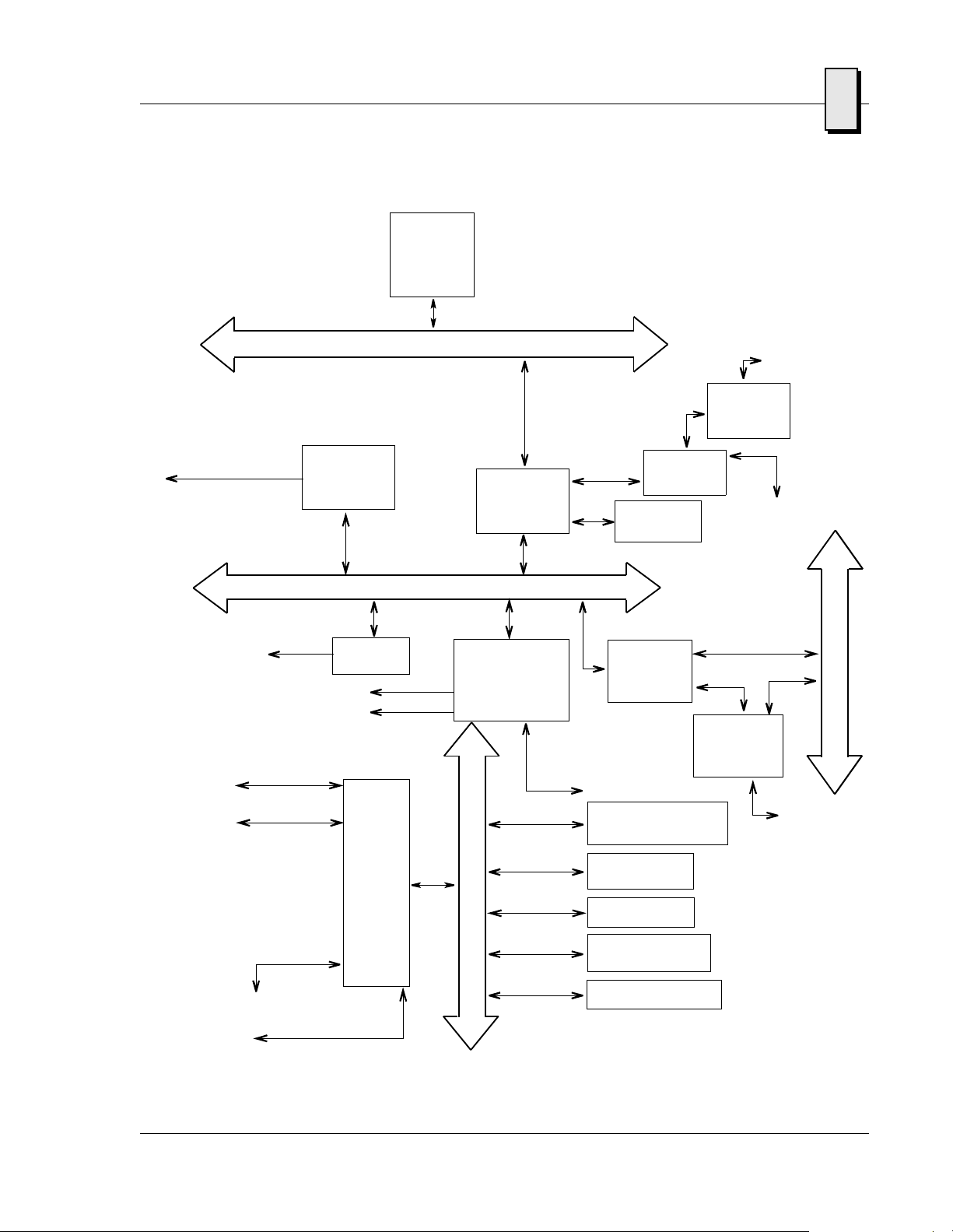
Pentium III
Processor
1
10BaseT/100Base Tx
J5
J5
J5
PMC I/O
J4
COM Port 1
COM Port 2
Floppy Drive
J5
Ethernet
Controller
Intel 82559ER
PMC Site
J5
J5
SUPER
I/O
with
RTC
FDC37C67X
Host bus
PCI bus
USB Port 0
USB Port 1
SMC
North Bridge
System
Controller
82443BX
South Bridge
PCI-to-ISA, IDE
Accelerator
Intel 82371EB (PIIX4E)
EIDE
Hard
Drive
I
S
A
b
u
s
AGP
Graphics
C&T 69030
SDRAM
PCI-to-PCI
Bridge
Intel 21154
J5
DiskOnChip
Socket
Optional
16 Bit Timers
82C54
Flash BIOS
Watchdog Timer
DS1384
Non Volatile SRAM
J4
LVDS
Trans
Custom Option
DS90C363A
Smbus
MUX
Philips PCA9540
J4
SVGA
J5
C
o
m
p
P
C
b
u
a
c
t
I
s
PS/2 Keyboard / Mouse
J5
Figure 1-1 VMICPCI-7715 Block D iag ram
25

1
VMICPCI-7715 Product Manual
CompactPCI Features
In addition to its PC/AT functions, the VMICPCI-7715 has the following CompactPCI
features:
• Single-slot, 6U height CPCI board
• Complies with Revision 2.1 of the PCI Local Bus Specification
• Complies with Revision 1.1 of the PCI-to-PCI Bridge Architecture Specification
(J1 pin B17 and C17 are used for Smbus Clock and Data respectively. J1 pin B17
and C17 are NOT used for SDONE and SB0# respectively.)
• Complies with Revision 2.1 of the CompactPCI Specification
• Implements delayed transactions for all PCI configuration, I/O and memory
read commands-up to three transactions simultaneously in each direction
• Allows 152 bytes of buffering (data and address) for upstream posted memory
write commands and 88 bytes of buffering for downstream posted memory
write commands - up to nine upstream and five downstream posted write
transactions simultaneously
• Allows 152 bytes of read data buffering upstream and 72 bytes of read data
buffering downstream
• Provides concurrent primary and secondary bus operation to isolate traffic
• Provides enhanced address decoding
• Includes addressing and VGA palette snooping support
• Supports PCI transaction forwarding for the following commands
- All I/O and memory commands
- Type 1 to Type 1 configuration commands
- Type 1 to Type 0 configuration commands (downstream only)
- All Type 1 to specia l cycle configuration commands
• Includes downstream lock support
• Supports both 5 and 3.3 V signaling environments
The VMICPCI-7715 is a versatile single-board solution for CPCI con trol with fam iliar
PC/AT operation.
VMICPCI-7715 Product Options
VMIC’s VMICPCI-7715 is built around three fundamental hardware configurations.
These configurations involve processor performance, the D iskOnChip, and SDRAM
memory size. These options are subject to change based on emerging technologies and
availability of vendor configurations.
The options and current details available with the VMICPCI-7715 are defined in the
device specification sheet available from your VMIC representative.
26

CompactPCI Features 1
27

1
VMICPCI-7715 Product Manual
28

Installation and Setup
Contents
Unpacking Procedures. . . . . . . . . . . . . . . . . . . . . . . . . . . . . . . . . . . . . . . . . . . . . . . 29
Hardware Setup . . . . . . . . . . . . . . . . . . . . . . . . . . . . . . . . . . . . . . . . . . . . . . . . . . . . 30
Installation . . . . . . . . . . . . . . . . . . . . . . . . . . . . . . . . . . . . . . . . . . . . . . . . . . . . . . . . . 34
CHAPTER
2
Introduction
This chapter describes the configurable hardware resister settings, rear I/O
definitions, installation, system setup and operation of the VMICPCI-7715.
Unpacking Procedures
Any precautions found in the shipping container should be observed. All items
should be carefully unpacked and thoroughly inspected for damage that might have
occurred during shipment. All claims arising from shipping damage sho uld be f iled
with the carrier and a complete report sent to VMIC Customer Service along with a
request for advice concerning the disposition of the damaged item(s).
CAUTION: Some of the components assembled on VMIC’s products may be sensitive
to electrostatic discharge, and damage may occur on boards that are subjected to a
high energy electrostatic field. When the board is placed on a bench for configuring,
etc., it is suggested that conductive material be inserted under the board to provide a
conductive shunt. Unused boards should be stored in the same protective boxes in
which they were shipped.
29

2
VMICPCI-7715 Product Manual
Hardware Setup
The VMICPCI-7715 is factory populated with user-specified options as part of the
VMICPCI-7715 ordering information. The CPU speed, SDRAM and DiskOnChip size
are not user-upgradable. To change these options, contact customer service to receive
a Return Material Authorization (RMA).
VMIC Customer Service is available at: 1-800-240-7782.
Or E-mail us at customer.s ervice@vmic.com
The VMICPCI-7715 is tested for system operation and shipped with factory-installed
configurable jumpers. The physical location of the jumpers for the SBC are illustrated
in Figure 2-1 on page 31. The definitions of the SBC board jumpers are included in
Table 2-2 through Table 2-6.
CAUTION: All jumpers are factory configured and should not be modified by the
user. There are four exceptions: the Password Clear (E24), the Watchdog Timer (E27),
Battery jumpers (E22 and E23) and Timer Clock Select (E28).
Modifying any other jumper will void the Warranty and may damage the unit. The
default jumper condition of the VMICPCI-7715 is expressed in Table 2-1 through
Table 2-5 with bold text in the table cells.
30

Located On
Reverse Side
Hardware Setup
2
Figure 2-1 VMICPCI-7715 Board Jumper Locations
31

2
VMICPCI-7715 Product Manual
Table 2-1 Board Connectors
Connector Function
CPCI J5 PS/2 Keyboard and Mouse, Smbus,
USB0 1, Ethernet, COM1, COM2, Floppy
Drive, IDE Harddrive
CPCI J4 PMC I/O, VGA Video, LVDS Video
.
Table 2-2 Watchdog Timer Select (User Configurable) - Jumper (E27)
Select Jumper Position
Watchdog Timer
RESET 1-2
NMI 2-3
No RESET or NMI Out
Table 2-3 BIOS Mode Option - Resister (R409)
Select Resister Position
No Boot Block Programming Out
Boot Block Programming In
NOTE: The VMICPCI-7715’s BIOS has the capability (Default: Disabled) of password
protecting casual access to the unit’s CMOS set-up screens. The Password Clear
jumper (E24) allows for a means to clear the password feature, which might be
necessary in the case of a forgotten password.
To clear the CMOS:
1. Turn off power to the unit.
2. Install a jumper at E24.
32
3. Power up the unit.
4. Turn off the power to the unit and remove jumper E24.
When power is re-applied to the unit, the CMOS will be cleared.

Table 2-4 Password Clear (User Configurable) - Jumper (E24)
Jumper Position
Normal Out
Clear CMOS/Password In
Table 2-5 CMOS Battery Enable (User Configurable) - Jumper (E23)
Jumper Position
CMOS Battery Disabled Out
CMOS Battery Enabled In
Hardware Setup
2
Table 2-6 Watchdog Battery Enable (User Configurable) - Jumper (E22)
Jumper Position
Watchdog Battery Disa bled Out
W atchdog Batte ry Enabled In
Table 2-7 Clock Select (User Configurable) - Jumper (E28)
Jumper Pos ition
1 MHz Out
2 MHz In
33

2
VMICPCI-7715 Product Manual
Installation
The VMICPCI-7715 conforms to the CompactPCI physical specification for a 6U
board. The VMICPCI-7715 is a system slot only board. It can be plugged directly into
any standard chassis accepting this type of board. The following pictures illustrate the
symbols used to identify the slots in a standard CPCI chassis.
This symbol identifies the System Controller slot
This symbol identifies peripheral slot
CAUTION: Do not install or remove the board while power is applied.
The following steps describe the VMIC recommended method for installation and
powerup of the VMICPCI-7715:
1. Make sure power to the equipment is off.
2. If a PMC module such as VMIC’s VMIPMC-7441 is to be used, connect it to the
VMICPCI-7715 prior to board installation. Refer to the Product Manual for that
particular board for configuration and setup.
3. The VMICPCI-7715 must be installed in the designated system slot of the CompactPCI backplane.
NOTE: The VMICPCI-7715 requires forced air cooling. It is advisable to install blank
panels over any exposed slots. This will allow for better ai r flow o ver the board.
4. Insert the VMICPCI-7715 into the CompactPCI ch assis system slot. While
ensuring that the board is properly aligned and oriented in the supporting boar d
guides, slide the board smoothly forward against the mating connector. Use the
ejector handles to firmly seat the board.
5. The VMICPCI-7715 features a DiskOnChip resident on the board. Refer to
Chapter 4 for set up details.
6. If an external drive module is installed, the BIOS Setup program must be run to
configure the drive types. See Appendix B to properly configure the system.
7. If a drive module is present, install the operating system according to the
manufacturer’s instructions.
34
8. A keyboard/mouse are required if the system has not been previously configured.

BIOS Setup
The VMICPCI-7715 has an on-board BIOS Setup program that controls many
configuration options. These options are saved in a special nonvolatile,
battery-backed memory chip and are collectively referred to as the board’s “CMOS
configuration.” The CMOS configura tion controls many details concerning the
behavior of the hardware from the moment power is applied.
The VMICPCI-7715 is shipped from the factory with no hard drives configured in
CMOS. The BIOS Setup program must be run to configure the specific drives
attached.
Details of the VMICPCI-7715 BIOS setup program are included in Appendix C.
PMC Expansion Site Co nnecto rs
The VMICPCI-7715 supplies PMC expansion site connectors for adding a PMC
expansion board. This expansion capability allows third-party devices to be used with
the VMICPCI-7715, as shown in Figure 2-2.
Installation
2
VMICPCI-7715
*There are 64 bits connected to the PMC I/O through J4
Figure 2-2 PCI Expansion Site
PCI
PMC I/O*
CompactPCI
PMC Expansion
Site
Power
Only
35

2
VMICPCI-7715 Product Manual
36

PC/AT Functions
Contents
CPU Socket. . . . . . . . . . . . . . . . . . . . . . . . . . . . . . . . . . . . . . . . . . . . . . . . . . . . . . . . . 38
Physical Memory . . . . . . . . . . . . . . . . . . . . . . . . . . . . . . . . . . . . . . . . . . . . . . . . . . . 38
Memory and Port Maps. . . . . . . . . . . . . . . . . . . . . . . . . . . . . . . . . . . . . . . . . . . . . . 39
PC/AT Interrupts . . . . . . . . . . . . . . . . . . . . . . . . . . . . . . . . . . . . . . . . . . . . . . . . . . . 42
PCI Interrupts . . . . . . . . . . . . . . . . . . . . . . . . . . . . . . . . . . . . . . . . . . . . . . . . . . . . . . 46
I/O Ports . . . . . . . . . . . . . . . . . . . . . . . . . . . . . . . . . . . . . . . . . . . . . . . . . . . . . . . . . . 47
Video Graphics Adapter . . . . . . . . . . . . . . . . . . . . . . . . . . . . . . . . . . . . . . . . . . . . . 48
Ethernet Controller. . . . . . . . . . . . . . . . . . . . . . . . . . . . . . . . . . . . . . . . . . . . . . . . . . 49
CHAPTER
3
Introduction
The VMICPCI-7715 provides a complete Pentium III processor-based Single Board
Computer (SBC). The design includes a high-speed microprocessor with current
technology memory .
Because the design is PC/AT compatible, it retains standard PC memory and I/O
maps along with standard interrupt architecture. Furthermore, the VMICPCI-7715
includes a PCI-compatible video adapter and Ethernet controller.
The following sections describe in detail the PC/AT functions of the VMICPCI-7715.
37

3
VMICPCI-7715 Product Manual
CPU Socket
The VMICPCI-7715 CPU socket is factory populated with a high-speed Pentium
III processor. The CPU type or speed, SDRAM size and DiskOnChip size are
user-specified as part of the VMICPCI-7 715 o r dering information. The options are not
user-upgradable.
To change CPU type or speeds, SDRAM size or DiskOnChip size contact VMIC
customer service to obtain a Return Material Authorization (RMA).
VMIC Customer Service is available at: 1-800-240-7782.
Or E-mail us at customer.s ervice@vmi c.com
Physical Memory
The VMICPCI-7715 provides 512 Mbytes of Synchronous DRAM (SDRAM) as
on-board system memory. Memory can be accessed as bytes, words or longwords.
All RAM on the VMICPCI-7715 is dual-ported to the CompactPCI bus through the
PCI-to-PCI bridge. The memory is addressable by the local processor, as well as the
CompactPCI bus slave interface by another CompactPCI master. Caution must be
used when sharing memory between the local processor and the CompactPCI bus to
prevent a CompactPCI bus master from overwriting the local processor’s operating
system.
The VMICPCI-7715 includes the system BIOS, and video BIOS in a single flash
memory device.
The VMICPCI-7715 is also a vail able wi th an opti onal MS yst ems D iskO nChip f lash up
to 288 Mbytes.
38

Memory and Port Maps
Memory Map
The memory map for the VMICPCI-7715 is shown in Table 3-1. All systems share this
same memory map, although a VMICPCI-7715 with less than the full 512 Mbyte of
SDRAM does not fill the entire space reserved for On-Board Extended Memory.
Table 3-1 VMICPCI-7715, Interface Memory Address Map
Memory and Port Maps
3
MODE
PROTECTED MODE
REAL MODE
* This space can be used to set up protected mode PCI-to-CompactPCI bus windows (also referred
to as PCI slave images).
** This space can be allocated as shared memory (for example, between the processor-based CPU
and CompactPCI bus Master). Note, that if a PMC board is loaded, the expansion BIOS may be
placed in this area.
MEMORY ADDRESS
RANGE
$FFFF 0000 - $FFFF FFFF 64 Kbyte ROM BIOS Image
$0400 0000 - $FFFE FFFF 3.9 Gbyte Unused *
$0010 0000 - $0FFF FFFF 255 Mbyte Reserved for **
$E0000 - $FFFF F 138 Kbytes ROM BIOS
$D8010 - $DFFFF 32Kbytes
$D800E - $D800F 2 Kbyte Board ID
$D8000 - $D800D 14 bytes RTC/Watchdog Timer Control
$C8000 - $D7FFF 64 Kbyte LANWorks BIOS
$C0000 - $C7F FF 32 Kbyte Video ROM
$A0000 - $BFFFF 128 Kbyte Video RAM
$00000 - $9FFFF 640 Kbyte User RAM/DOS RAM
SIZE DESCRIPTION
On-Board Extended Memory
(not filled on all systems)
Non-volatile SRAM
minus 16 bytes
Registers
I/O Port Map
The Pentium III processor-based CPU includes special input/output instructions that
access I/O peripherals residing in I/O addressing space (separate and distinct from
memory addressing space). Locations in I/O address space are referred to as ports.
When the CPU decodes and executes an I/O instruction, it produces a 16-bit I/O
address on lines A00 to A15 and identifies the I/O cycle to the processor’s M/I/O
control line. Thus, the CPU includes an independent 64 Kbyte I/O address space,
which is accessible as bytes, words or longwords.
39

3
VMICPCI-7715 Product Manual
Standard PC/AT hardware circuitry reserves only 1,024 bytes of I/O addressing
space from I/O $000 to $3FF for peripherals. All standard PC I/O peripherals such as
serial and parallel ports, hard and floppy drive controllers, video system, real-time
clock, system timers, and interrupt controllers are addressed in this region of I/O
space. The BIOS initializes and configures all these registers properly; adjusting these
I/O ports directly is not normally necessar y.
The assigned and user-available I/O addresses are summarized in the I/O Address
Map, Table 3-2.
Table 3-2 VMICPCI-7715 I/O Address Map
I/O ADDRESS
RANGE
$000 - $00F 16 DMA Controller 1
$010 - $01F 16 Reserved
$020 - $021 2 Master Interrupt Controller
$022 - $03F 30 Reserved
$040 - $043 4 Programmable Timer
$044 - $05F 30 Reserved
$060 - $064 5 Keyboard, Speaker, Eqpt. Configuration
$065 - $06F 11 Reserved
$070 - $071 2 Real-Time Clock, NMI Mask
$072 - $07F 14 Reserved
$080 - $08F 16 DMA Page Registers
$090 - $091 2 Reserved
SIZE IN
BYTES
HW DEVICE PC/AT FUNCTION
(Intel 8237A Compatible)
(Intel 8259A Compatible)
(Intel 8254 Compatible)
(Intel 8042 Compatible)
40
$092 1 Alt. Gate A20/Fast Reset Register
$093 1 Reserved
$094 1 Super VGA Chip POS102 Access Control Register
$095 - $09F 11 Reserved
$0A0 - $0A1 2 Slave Interrupt Controller
(Intel 8259A Compatible)
$0A2 - $0BF 30 Reserved
$0C0 - $0DF 32 DMA Controller 2
(Intel 8237A Compatible)

Memory and Port Maps
Table 3-2 VMICPCI-7715 I/O Address Map (Continued)
3
I/O ADDRESS
RANGE
$0E0 - $16F 142 Reserved
$170 - $177 8 PIIX4E Secondary Hard Disk Controller
$178 - $1EF 120 User I/O
$1F0 - $1F7 8 PIIX4E Primary Hard Disk Controller
$1F8 - $277 128 User I/O
$278 - $27F 8 Super I/O Chip* LPT2 Para llel I/O*
$280 - $2E7 104 Reserved
$2E8 - $2EE 7 UART* COM4 Serial I/O*
$2EF - $2F7 9 User I/O
$2F8 - $2FE 7 Super-I /O C hip COM2 Serial I/O (16550 Compatible)
$2FF - $36F 113 Reserved
$370 - $377 8 Super-I/O Chip Secondary Floppy Disk Controller
$378 - $37F 8 Super-I/O Chip LPT1 Para llel I/O
$380 - $3E7 108 Reserved
$3E8 - $3EE 7 UART* COM3 Serial I/O*
SIZE IN
BYTES
HW DEVICE PC/AT FUNCTION
$3F0 - $3F7 8 Super-I/O Chip Primary Floppy Disk Controller
$3F8 - $3FE 7 Super-I /O Chip COM1 Serial I/O (16550 Compatible)
$3FF - $4FF Reserved
$500 - $503 4 82C54 Timer Programmable Internal Timer
$504 - $CFF Reserved
* While these I/O ports are reserved for the listed functions, they are not implemented on
the VMICPCI-7715. They are listed here to make the user aware of the standard
PC/AT usage of these ports.
PCI-to-PCI Bridge
The VMICPCI-7715 uses the Intel 21154 PCI-to-PCI bridge to interface between the
primary PCI bus of the unit and the CompactPCI (CPCI) bus. The CompactPCI bus
appears as a secondary PCI bus, and all devices in the seven peripheral slots of the
CPCI chassis are auto detected by the BIOS and respond to normal PCI accesses.
41

3
VMICPCI-7715 Product Manual
PC/AT Interrupts
In addition to an I/O port address, an I/O device has a separate hardware interrupt
line assignment. Assigned to each interrupt line is a corresponding interrupt vector in
the 256-vector interrupt table at $00000 to $003FF in memory. The 16 maskable
interrupts and the single Non-Maskable Interrupt (NMI) are listed in Table 3-3 along
with their functions. Table 3-4 on page 43 details the vectors in the interrupt vector
table. The interrupt number in HEX and decimal are also defined for real and
protected mode in Table 3-4.
The interrupt hardware implementation on the VMICPCI-7715 is standard for
computers built around the PC/AT architecture, which evolved fr om the IBM PC/XT.
In the IBM PC/XT computers, only eight interrupt request lines exist, numbered fr o m
IRQ0 to IRQ7 at the PIC. The IBM PC/AT computer added eight more IRQx lines,
numbered IRQ8 to IRQ15, by cascading a second slave PIC into the original master
PIC. IRQ2 at the master PIC was committed as the cascade input from the slave PIC.
This architecture is represented in Figure 3-1 on page 47.
To ma intain backward compatibility with PC/XT systems, IBM chose to use the new
IRQ9 input on the slave PIC to operate as the old IRQ2 interrupt line on the PC/XT
Expansion Bus. Thus, in AT systems, the IRQ9 interrupt line connects to the old IRQ2
pin (pin B4) on the AT Expansion Bus (or ISA bus).
Table 3-3 PC/AT Hardware Interrupt Line Assignments
IRQ AT FUNCTION COMMENTS
NMI Parity Errors
(Must be enabled in BIOS Setup)
0 System Timer Set by BIOS Setup
1 Keyboard Set by BIOS Setup
2 Duplexed to IRQ9
3 COM2/COM4
4 COM1/COM3
5 General Purpose Timer Assigned to On-Board Timer
6 Floppy Controller
7 Not Assigned Determined by BIOS
8 Real-Time Clock
9USB
Used by VMICPCI-7715
CompactPCI bus Interface
42

PC/AT Interrupts
Table 3-3 PC/AT Hardware Interrupt Line Assignments (Continued)
IRQ AT FUNCTION COMMENTS
10 Not Assigned Determined by BIOS
11 Not Assigned Determined by BIOS
12 Mouse
13 Math Coprocessor
14 AT Hard Drive
15 Not Assigned Determined by BIOS
Table 3-4 PC/AT Interrupt Vector Table
3
INTERRUPT NO.
HEX DEC
00 0 Divide Error Same as Real Mode
01 1 Debug Single Ste p Same as Real Mode
02 2 NMI Memory Parity Error Same as Real Mode
03 3 Debug Breakpoint Same as Real Mode
04 4 ALU Overflow Same as Real Mode
05 5 Print Screen Array Bounds Check
06 6 Invalid OpCode
07 7 Device Not A v ailable
08 8 IRQ0 Timer Tick Double Exception Detected
09 9 IRQ1 Keyb oar d Input Coprocessor Segment Overrun
0A 10 IRQ2 BIOS Reserved Invalid Task State Segment
0B 11 IRQ3 COM2 Serial I/O Segment Not Present
0C 12 IRQ4 COM1 Serial I/O Stack Segment Overrun
IRQ
LINE
REAL MODE PROTECTED MODE
(Must be enabled in BIOS Setup)
0D 13 IRQ5
0E 14 IRQ6 Floppy Disk Controller Page Fault
0F 15 IRQ7 Assigned by BIOS
43

3
VMICPCI-7715 Product Manual
Table 3-4 PC/AT Interrupt Vector Table (Continued)
INTERRUPT NO.
HEX DEC
10 16 BIOS Video I/O Coprocessor Error
11 17 Eqpt Configuration Check Same as Real Mode
12 18 Memory Size Check Same as Real Mode
13 19 XT Floppy/Hard Drive Same as Real Mod e
14 20 BIOS Comm I/O Same as Real Mode
15 21 BIOS Cassette Tape I/O Same as Real Mode
16 22 BIOS Keyboard I/O Same as Real Mode
17 23 BIOS Printer I/O Same as Real Mode
18 24 ROM BASIC Entry Point Same as Real Mode
19 25 Bootstrap Loader Same as Real M ode
1A 26 IRQ8 Real-Time Clock Same as Real Mode
1B 27 Control/Break Handler Same as Real Mode
1C 28 Timer Control Same as Real Mode
IRQ
LINE
REAL MODE PROTECTED MODE
1D 29 Video Parameter Table Pntr Same as Real Mode
1E 30 Floppy Parm Table Pntr Same as Real Mode
1F 31 Video Graphics Table Pntr Same as Real Mode
20 32 DOS Terminate Program Same as Real Mode
21 33 DOS Function Entry Point Same as Real Mode
22 34 DOS Terminate Handler Same as Real Mode
23 35 DOS Control/Break Handler Same as Real Mod e
24 36 DOS Critic al Error Handler Same as Real Mode
25 37 DOS Absolute Disk Read Same as Real Mode
26 38 DOS Absolute Disk Write Same as Real Mode
27 39 DOS Program Terminate,
Stay Resident
28 40 DOS Keyboard Idle Loop Same as Real Mod e
29 41 DOS CON Dev. Raw Output Same as Real Mode
Same as Real Mode
44

Table 3-4 PC/AT Interrupt Vector Table (Continued)
PC/AT Interrupts
3
INTERRUPT NO.
HEX DEC
2A 42 DOS 3.x+ Network Comm Same as Real Mode
2B 43 DOS Internal Use Same as Real Mode
2C 44 DOS Internal Use Same as Re al Mode
2D 45 DOS Internal Use Same as Real Mode
2E 46 DOS Internal Use Same as Real Mode
2F 47 DOS Print Spooler Driver Same as Real Mode
30-60 48-9 6 R eserved by DOS Same as Real Mo de
61-66 97-1 02 User Available Same as Real Mode
67-70 103- 112 Reserved by DOS Same as Real Mode
71 113 IRQ 9 USB
72 114 IRQ10 Assigned by BIOS
73 115 IRQ11 Assigned by BIOS
74 116 IRQ12 Mouse
IRQ
LINE
REAL MODE PROTECTED MODE
75 117 IRQ13 Math Coprocessor
76 118 IRQ14 AT Hard Drive
77 119 IRQ15 Assigned by BIOS
78-7F 120-127 Reserved by DOS Same as Real M ode
80-F0 128-240 Reserved for BASIC Same as Real Mode
F1-FF 241-255 Reserved by DOS Same as Real Mo de
45

3
VMICPCI-7715 Product Manual
PCI Interrupts
Interrupts on Peripheral Component Interconnect (PCI) Local Bus are optional and
defined as “level sensitive,” asserted low (negative true), using open drain output
drivers. The assertion and de-assertion of an interrupt line, INTx#, is asynchronous to
CLK. A device asserts its INTx# line when requesting attention from its device driver.
Once the INTx# signal is asserted, it remains asserted until the device driver clears the
pending request. When the request is cleared, the device de-asserts its INTx# signal.
PCI defines one interrupt line for a single function device, and up to four interrupt
lines for a multifunction device or connector. For a single function device, only INTA#
may be used while the other three interrupt lines have no meaning. Figure 3-1 on
page 47 depicts the VMICPCI-7715 interrupt logic pertaining to CompactPCI bus
operations and the PCI expansion site.
Any function on a multifunction device can be connected to any of the INTx# lines.
The Interrupt Pin register defines which INTx# line the function uses to request an
interrupt. If a device implements a single INTx# line, it is called INTA#; if it
implements two lines, they are called INTA# and INTB#; and so forth. For a
multifunction device, all functions may use the same INTx# line, or each may have its
own (up to a maximum of four functions), or a ny combination thereof. A single
function can not generate an interrupt request on more than one INTx# line.
Table 3-5 NMI Register Bit Descriptions
Status Control Register
(I/O Address $061, Read/Write, Read Only)
SERR# NMI Source Status (Read Only) - This bit is set to 1 if a system board agent
Bit 7
Bit 2 PCI SERR# Enable (Read/Write) - 1 = Clear and Disable, 0 = Enable
Bit 7 NM I Enable - 1 = Disab le, 0 = Enable
detects a system board error. It then asserts the PCI SERR# line. To reset the interrupt,
set bit 2 to 0 and then set it to 1. When writing to port $061, bit 7 must be 0.
Enable and Real-Time Clock Address Register
(I/O Address $070, Write Only)
46

I/O Ports
I/O Ports
3
The VMICPCI-7715 incorporates the SMC Super-I/O chip. The SMC chip provides the
VMICPCI-7715 with a standard floppy drive controller and two 16550
UART-compatible serial ports. The Ultra-IDE hard drive interface is provided by the
Intel 82371EB (PIIX4E) PCI ISA IDE Xcelerator chip. All ports are present in their
standard PC/AT locations using default interrupts.
INTR
Keybd
Timer
INT
IRQ0 IRQ1
Real-Tm
Clock
USB
IRQ8 IRQ9
IRQ8
PCI ISA IDE
Xcellerator
The PCI-to-ISA Bridge
PIIX4E 82371EB
INTA
PMC
Site
INTB
INTC
INTD
CPU
8259 MASTER-
Interrupt
8-15
Com 2
IRQ2 IRQ4 IRQ5
IRQ10
IRQ10IRQ9
CONNECTIONS
MAPPED BY BIOS
PCI INTERRUPT
PIRQ0 PIRQ1 PIRQ2 PIRQ3
Com 1
GP
Timers
8259 SLAVE-
Mouse Math
NANA
IRQ11 IRQ13
IRQ11
MAPPER
IRQ12
IRQ12
PORTS $020-$021
Floppy
Control
IRQ6IRQ3
PORTS $0A0-$0A1
AT
Hard Drv
Coproc
Watchdog
N/A
IRQ7
N/A
IRQ14 IRQ15
IRQ14IRQ13
IRQ15
SERR
INTA
INTB
INTC
INTD
C
P
C
I
b
u
s
SVGA
INTA
Connection
Not Complete
INT
Ethernet
PCI-to-PCI
BRIDGE
Bus
Figure 3-1 Connections for the PC Interrupt Logic Controller
47

3
VMICPCI-7715 Product Manual
Video Graphics Adapter
The monitor port on the VMICPCI-7715 is controlled by a Chips and Technology
69030 video adapter chip with 4 Mbyte video SGRAM. The video controller chip is
hardware and BIOS compatible with the IBM EGA and SXGA standards and also
supports VESA high-resolution and extended video modes. Table 3-6 shows the
graphics video modes supported by the VMICPCI-7715.
Table 3-6 Supported Graphics Video Resolutions
SCREEN
RESOLUTION
640 x 480 16 M 60, 75, 85
800 x 600 16 M 60, 75, 85
1024 x 768 64 K 60, 75, 85
1280 x 1024 256 60, 75
Not all SVGA monitors support resolutions and refresh rates beyond 640 x 480 at
60 Hz. Do not attempt to drive a monitor to a resolution or refresh rate beyond its
capability.
MAXIMUM
COLORS
REFRESH RATES
(Hz)
48

Ethernet Controller
The network capability is provided by Intel’s 82559ER. This Ethern et con tr o ller is PCI
bus based and is software configurable. The VMICPCI-7715 supports 10BaseT a nd
100BaseTx Ethernet.
10BaseT
A network based on the 10BaseT standard uses unshielded twisted-pair cables,
providing an economical solution to networking by allowing the use of existing
telephone wiring and connectors.
100BaseTx
The VMICPCI-7715 also supports the 100BaseTx Ethernet. A network based on a
100BaseTx standard uses Category 5 unshielded twisted-pair cables.
Ethernet Controller
3
49

3
VMICPCI-7715 Product Manual
50

CHAPTER
Embedded PC/RTOS Features
Contents
DiskOnChip (Optional). . . . . . . . . . . . . . . . . . . . . . . . . . . . . . . . . . . . . . . . . . . . . . . 52
Watchdog Timer. . . . . . . . . . . . . . . . . . . . . . . . . . . . . . . . . . . . . . . . . . . . . . . . . . . . . 54
Timers . . . . . . . . . . . . . . . . . . . . . . . . . . . . . . . . . . . . . . . . . . . . . . . . . . . . . . . . . . . . . 60
Battery Backed SRAM. . . . . . . . . . . . . . . . . . . . . . . . . . . . . . . . . . . . . . . . . . . . . . . . 69
Smbus Multiplexer. . . . . . . . . . . . . . . . . . . . . . . . . . . . . . . . . . . . . . . . . . . . . . . . . . . 70
4
Introduction
VMIC’s VMICPCI-7715 features additional capabilities beyond those of a typical IBM
PC/AT-compatible CPU. The unit provides three software-controlled, general
purpose timers in addition to a programmable Watchdog Timer. The VMICPCI-7715
also provides a bootable DiskOnChip and 32 Kbytes of Nonvolatile SRAM.
Additionally the VMICPCI provides access to the on-board Smbus via a Smbus
Multiplexer. These features make the unit ideal for embedded applications,
particularly applications where standard hard drives and floppy disk drives cannot
be used.
51

4
VMICPCI-7715 Product Manual
DiskOnChip (Optional)
The VMICPCI-7715 is available with an optional single DiskOnChip which is plugged
into a standard 32-pin socket. The DiskOnChip is mapped into a 32 Kbyte window in
the BIOS expansion address space of the PC, which is located between address
0xD0000 to 0xD1FFF.
The DiskOnChip contains a built- in copy of the M-Systems industry-stan d ard
T rueFFS software, which makes the DiskOnChip operate as a standard disk drive. The
DiskOnChip can contain the operating system in it to allow systems to boot without a
hard disk. The DiskOnChip can also be configured as the boot device in systems with
a hard disk.
Installing the DiskOnChip
1. To install the DiskOnChip as drive C on a system witho ut a hard disk, set the
CMOS setup of the Primary Master and Primary Slave to Not Installed
(indicating that no physical magnetic disk is installed), and reboot the computer.
The DiskOnChip will install as drive C. The DiskOnChip needs to be formatted
with the System files in order for it to be a bootable drive. See “Configuring the
DiskOnChip as the Boot Device” below.
2. To install the DiskOnChip as a logical drive on a system with a hard disk, just
reboot the system, and the DiskOnChip will install as the last drive.
NOTE: The active (bootable) partition will alw ays be drive C.
Configuring th e DiskOnChip as t he Boot D evice
In order to configure the DiskOnChip as the boot device, the operating system files
need to be copied into the chip. Copying the operating system files into the
DiskOnChip should be done in the same manner as any other hard disk. The
following is a example of a typical initia lization process:
1. Set the DiskOnChip as a regular drive in your system (not a boot drive).
2. Insert a bootable floppy diskette in drive A and boot the system.
3. At the DOS prompt, type SYS C: to transfer the DOS system files to the
DiskOnChip (assuming the DiskOnChip is installed as drive C).
4. Copy any files needed into the DiskOnChip.
5. Remove the floppy diskette and reboot the system. The system will boot from
the DiskOnChip and will allow yo u to ru n and access any files that have been
copied into the DiskOnChip.
52

Using the DiskOnChip with Other Operating Systems
If the VMICPCI-7715 is to be used with a DiskOnChip running an operating system
other than DOS, the user should access the MSystems website at www.m-sys.com for
information on installation and other details.
DiskOnChip (Optional)
4
53

4
VMICPCI-7715 Product Manual
Watchdog Timer
The VMICPCI-7715 uses a Dallas DS1384 Watchdog Timekeeping Controller as its
Watchdog Timer. The device provides a Time of Day feature and a Watchdog Alarm.
The Time of Day feature found within the DS1384 device is explained in this section,
but is not utilized by the VMICPCI-7715. The actual Time of Day registers used by the
VMICPCI-7715 are located at the standard PC/AT I/O address. The Time of Day
feature in the DS1384 Watchdog Timer is available for use by the user at their
discretion. The Watchdog Timer provides a Watchdog Alarm window and interval
timing between 0.01 and 99.99 seconds.
NOTE: The Watchdog Timer Interrupt output must be set to Level Mode (see
Watchdog Command Register Bit 4) to use this option.
In addition, the Watchdog Alarm is connected via a two state header to either or
neither of the CPU reset or the system NMI. The user can direct the Watchdog Alarm
to reset the CPU if the jumper is set in the 1-2 posi tion; to initiate a Non-Maskable
Interrupt (NMI) the jumper is set in the 2-3 position; or neither if jumper is removed.
Figure 4-1 shows a generalized block diagram of how the Watchdog Timer is used in
the VMICPCI-7715. The Watchdog Timer registers are memory-mapped at addresses
$D8000 through $D800D. Table 4-1 shows the address, content and the range of each
Watch dog Register.
CPU
WATCHDOG
TIMER
INT
Figure 4-1 Watchdog Alarm Block
E27
1
2
3
Reset
NMI
54

Watchdog Timer
Table 4-1 Watchdog Registers
Register Address Bit 7 Bit 6 Bit 5 Bit 4 Bit 3 Bit 2 Bit 1 Bit 0 Range
0 $D8000 0.1 Seconds (BCD) 0.01 Seconds (BCD) 00 - 99
1 $D8001 10 Seconds (BCD) Seconds (BCD) 00 - 59
2 $D8002 10 Minutes (BCD) Minutes (BCD) 00 - 59
3 $D8003 M 10 Minute Alarm (BCD) Minute Alarm (BCD) 00 - 59
4 $D8004 0 12/24 AM/PM* 10 Hr Hours (BCD)
5 $D8005 M 12/24 AM/PM* 10 Hr Hour Alarm (BCD)
6 $D8006 0 0 0 0 Days (BCD) 01 - 07
7 $D8007 M 0 0 0 Day Alarm (BCD ) 01 - 07
8 $D8008 0 0 10 Date (BCD) Date (BCD) 01 - 31
4
9 $D8009 Eosc 1** 0 10 Mo Months (BCD) 01 - 12
A $D800A 1 0 Years (BCD) Years (BCD) 00 - 99
B $D800B Te Ipsw Ibh/lo Pu/lvl Wam Tdm Waf Tdf
C $D800C 0.1 Seconds (BCD) 0.01 Seconds (BCD) 00 - 99
D $D800D 10 Seconds (BCD) Seconds (BCD) 00 - 99
* In the 12 hour mode Bit 5 determines AM (0) or PM (1). In the 24 hour mode Bit 5 combines with Bit 4 to represent the
10 hour value.
** Bit 6 of Register 9 must be set to a 1. If set to a 0, an unused square wave will be generated in the circuit.
Registers 0 through A are Clock, Calendar, Time of Day Registers.
Register B is the Command Register.
Registers C and D are Watchdog Alarm Registers.
The Watchdog Timer contains 14 registers which are 8-bits wide. These registers
contain all of the Tim e of Day, Alarm, Watchdog, Control and Data information. The
Clock Calendar, Alarm and Watchdog Registers have both external (user accessi ble)
and internal memory locations containing copies of the data. The external memory
locations are independent of the internal functions except they are updated
periodically by the transfer of the incremented internal values. Registers 0, 1, 2, 4, 6, 8,
9 and A contain Time of Day and Data information in Binary Coded Decimal (BCD).
Registers 3, 5 and 7 contain the Time of Day Alarm information in BCD. The
Command Register (Register B) contains data in binary. The Watchdog Alarm
Registers are Registers C and D, and information stored in these registers is in BCD.
55

4
VMICPCI-7715 Product Manual
Time of Day Registers
Registers 0, 1, 2, 4, 6, 8, 9 and A contain Time of Day data in BCD.
Register 0 contains two Time of Day values. Bits 3 - 0 contain the 0.01 Seconds value
with a range of 0 to 9 in BCD while Bits 7 - 4 contain the 0.1 Seconds value with a
range of 0 to 9 in BCD. This register has a total range of 0.00 to 0.99 Seconds.
Register 1 contains two Time of Day values. Bits 3 - 0 contain the 1 Seconds value with
a range of 0 to 9 in BCD while Bits 7 - 4 conta in the 10 Seconds value with a range of 0
to 5 in BCD. This register has a total range of 0.0 to 59.0 Seconds. Bit 7 of this register
will always be zero regardless of what value is written to it.
Register 2 contains two Time of Day values. Bits 3 - 0 contain the 1 Minute value with a
range of 0 to 9 in BCD, Bits 7 - 4 contain the 10 Minutes value with a range of 0 to 6 in
BCD. This register has a total range of 0 to 59 Minutes. Bit 7 of this register will always
be zero regardless of what value is written to it.
Register 4 contains the Hours value of the Time of Day. The Hours can be represented
in either 12- or 24-hour format depending on the state of Bit 6. When Bit 6 is set to a
one (1) the format is 12-hour. When Bit 6 is set to a zero (0) the format is 24-hour. For
the 12-hour format Bits 3 - 0 contain the 1-hour value with a range of 0 to 9 in BCD
and Bit 4 contains the 10-hour value with a range of 0 to 1. In the 12-hour format Bit 5
is used as the AM/PM bit. For AM, Bit 5 is set to zero (0) and for PM, Bit 5 is set to one
(1). The total range of this register in the 12 hour f ormat is 01 AM to 12 AM an d 01 PM
to 12 PM.
When Register 4 is in 24-hour format (Bit 6 is set to a zero (0)) Bits 3 - 0 contain the
1-hour value with a range of 0 to 9 in BCD, Bit 5 combines with 4 to represent the
10-hour value. The 10-hour range is from 0 to 2. The total range of Register 4 in th e
24-hour format is 00 to 23 hours. Bit 7 of Register 4 will always be zero regardless of
what value is written to it and regardless of format (12- or 24-hour).
Register 6 contains the Days value of the Time of Day. Bits 2 - 0 contain the Days value
with a range of 1 to 7 in BCD.
Register 8 contains two Time of Day values. Bits 3 - 0 contain the Date value with a
range of 0 to 9 in BCD while Bits 5 - 4 contain the 10 Date value with a range of 0 to 3.
This register has a total range of 01 to 31. Bits 7 - 6 of this register will always be zero
regardless of what value is written to it.
Register 9 contains two Time of Day values. Bits 3 - 0 contain the Months value with a
range of 0 to 9 in BCD while Bits 4 contain the 10 Date value with a range of 0 to 1.
This Register has a total range of 01 to 12. Bit 5 will always be zero regardless of what
value is written to it. Bit 6 is unused but must be set to a 1. Bit 7, Eosc
oscillator enable bit. When this bit is set to a zero (0) the oscillator is internally
enabled. When set to a one (1) the oscillator is internally disabled. The oscillator via
this bit is usually turned on once during system initialization, but can be toggled on
and off at the user’s discretion.
, is the clock
56

There are two techniques for reading the Time of Day from the Watchdog Timer. The
first is to halt the external Time of Day registers from tracking the internal Time of
Day registers by setting the Te bit (Bit 7 of the Command Register) to a logic zero (0),
then reading the contents of the Time of Day registers. Using this technique eliminates
the chance of the Time of Day changing while the read is taking place. At the end of
the read, the Te bit is set to a logic one (1) allowing the external Time of Day registers
to resume tracking the internal Time of Day registers. No time is lost as the internal
Time of Day registers continue to keep time while the external Time of Day registers
are halted. This is the recommended method.
The second technique for reading the Ti me of Day from the Watchdog Timer is to read
the external Time of Day registers without halting the tracking of the internal
registers. This is not recommended as the registers may be updated while the reading
is taking place, resulting in erroneous data being read.
Time of Day Alarm Registers
Registers 3, 5 and 7 are the Time of Day Alarm registers and are formatted similar to
Register 2, 4 and 6 respectively. Bit 7 of Registers 3, 5 and 7 is a mask bit. The mask
bits, when active (logic one (1)), disable the use of the particular Time of Day Alarm
register in the determination of the Time of Day Alarm (see Table 4-2). When all the
mask bits are low (0) an alarm will occur when Registers 2, 4 and 6 match the values
found in Registers 3, 5 and 7. When Register 7’s mask bit is set to a lo gic one (1),
Register 6 will be disregarded in the determination of the Time of Day Alarm and an
alarm will occur everyday. When Registers 7 and 5’s mask bit is set to a logic one (1),
Register 6 and 4 will be disregarded in the determination of the Time of Day Alarm
and an alarm will occur every hour. When Registers 7, 5 and 3’s mask bit is set to a
logic one (1), Register 6, 4 and 2 will be disregarded in the determination of the Time
of Day Alarm and an alarm will occur every minute (when register 1’s seconds step
from 59 to 00).
Watchdog Timer
4
Table 4-2 Time of Day Alarm Registers
Register Comment
Minutes Hours Days
1 1 1 Alarm once per minute
0 1 1 Alarm when minutes match
0 0 1 Alarm when hours and minutes match
0 0 0 Alarm when hours, minutes, and days match
The Time of Day Alarm registers are read and written to in the same format as the
Time of Day registers. The T ime of Day Alarm flag and interrupt are cleared when the
alarm registers are read or written.
57

4
VMICPCI-7715 Product Manual
Watchdog Alarm Registers
Register C cont ains two Watchdog Alarm values. Bits 3 - 0 contain the 0.01 Seconds
value with a range of 0 to 9 in BCD while Bits 7 - 4 contain the 0.1 Seconds value with
a range of 0 to 9 in BCD. This register has a total range of 0.00 to 0.99 Seconds.
Register D contains two Watchdog Alarm values. Bits 3 - 0 contain the 1 Second value
with a range of 0 to 9 in BCD while Bits 7 - 4 contain the 10 Seconds value with a range
of 0 to 9 in BCD. This register has a total range of 00.0 to 99.0 Seconds.
The W atchdog Alarm Registers can be read or written in any or der. When a new value
is entered or the Watchdog registers are read, the Watchdog Timer will start counting
down from the entered value. When zero is reached, the Watchdog Interrupt Output
will go active. If jumper J30 is loaded, the CPU will reset to a known state (Refer to
Figure 4-1). The Watchdog Timer count is reinitialized back to the entered value, the
Watchdog flag bit is cleared, and the Watchdog interrupt output is cleared every time
either of the registers is accessed. Periodic accesses to the Watchdog Timer will
prevent the Watchdog Alarm from occurring. If access does not occur, the alarm will
be repetitive. The Watchdog Alarm Register always reads the entered value. The
actual countdown value is internal and not accessible to the user. Writing zeroes to
Registers C and D will disable the Watchdog Alarm feature.
Command Register
Register B is the Command Register. Within this register are mask bits, control bits
and flag bits. The following paragraphs describe each bit.
Te - Bit 7 T ransfer Enable - This bit enables and disables the tracking of data between th e
internal and external registers. When set to a logic zero (0), tracking is disabled,
freezing the data in the external register. When set to a logic one (1), tracking is
enabled. This bit must be set to a logic one (1) to allow the external register to be
updated.
Ipsw - Bit 6 Interrupt Switch - This bit toggles the Interrupt Output between the Time of
Day Alarm and the Watchdog Alarm. When set to a logic zero (0), the Interrupt
Output is from the W atchdog Alarm. When set to a logic one (1), the Interrupt Output
is from the Time of Day Alarm.
Ibh/lo - Bit 5 Reserved - This bit should be set to a logic low (0).
Pu/lvl - Bit 4 Interrupt Pulse Mode or Level Mode - This bit determines whether the
Interrupt Output will output as a pulse or a level. When set to a logic zero (0),
Interrupt Output will be a level. When set to a logic one (1), Interrupt Output will be a
pulse. In pulse mode, the Interrupt Output will sink current for a minimum of 3 ms.
This bit should be set to a logic one (1).
Wam - Bit 3 Watch dog Alarm Mask - Ena bles/Disables the Watchdog Alarm to Interrupt
Output when Ipsw (Bit 6, Interrupt Switch) is set to logic zero (0). When set to a logic
zero (0), Watchdog Alarm Interrupt Output will be enabled. When set to a logic one
(1), Watchdog Alarm Interrupt Output will be disabled.
58

Watchdog Timer
Tdm - Bit 2 Time of Day Alarm Mask - Enables/Disables the Time of Day Alarm to
Interrupt Output when Ipsw (see Bit 6, Interrupt Switch) is set to logic one (1). When
set to a logic zero (0), Time of Day Alarm Interrupt Output will be enabled. When set
to a logic one (1), Time of Day Alarm Interrupt Output will be disabled.
Waf - Bit 1 Watchdog Alarm Flag - This is a read-only bit set to a logic one (1) when a
Watchdog Alarm Interrupt occurs. This bit is reset when any of the Watchdog Alarm
registers are accessed. When the Interrupt Output is set to Pulse Mode (see Bit 4,
Interrupt Pulse Mode or Level Mode), the flag will be set to a logic one (1) only when
the Interrupt Output is active.
Tdf - Bit 0 Time of Day Alarm Flag - This is a read-only bit set to a logic one (1) when a
Time of Day Alarm Interrupt occurs. This bit is reset when any of the Time of Day
Alarm registers are accessed. When the Interrupt Output is set to Pulse Mode (see Bit
4, Interrupt Pulse Mode or Level Mode), the flag will be set to a logic one (1) only
when the Interrupt Output is active.
4
59

4
VMICPCI-7715 Product Manual
Timers
General
The VMICPCI-7715 provides a user-pr ogrammable 82C54 intern al timer/counter. The
82C54 provides three independent, 16-bit timers, each operating at 1 or 2 MHz clock
speed determined by the configuration of jumper E28. These timers are com pletely
available to the user and are not dedicated to any PC/AT function. These timers may
be used to generate system interrupts.
Events can be timed by either polling the timers or generating a sy stem interrupt via
circuity external to the 82C54. The external circuity consists of logic which generates
the interrupt, and a Timer Interrupt Status register which indicates which of the three
Timers generated an interrupt.
The 82C54 timers are mapped at I/O addres s $500. The interrupt used by the Timers
is IRQ5. The Timer Interrupt Status register is available via the Power Management
I/O address space. The access to this space is explained in the “Timer Interrupt
Status” section below.
Timer Interrupt Status
A single interrupt, IRQ5, is used by all three Timers. A Timer Interrupt Status register
is provided in order to determine which Timer(s) initiated an interrupt. The interrupt
status register is a general-purpose input register located, external to the 82C54, at
offset 31h from the Power Management Base I/O address. The interrupt status
register address can be f ound by first determining the PCI Conf iguration Base addr ess
for Device ID 7113h and Vendor ID 8086h. The Power Management Base I/O address
can be found by reading offset 40h from this PCI Configuration address. The Timer
Interrupt Status register bits are located at offset 31h from the Power Management
Base I/O address, Bits 5, 6 and 7 (refer to Figure 4-3).
Step 1: Read
South Bridge PCI
Configuration Base Address
Step 2: Read
Device ID 7113h
Vendor ID 8086h
Power Management
Base I/O Address
Step 3: Read
South Bridge PCI
Configuration Base
Address Ofset 40h
Timer Interrupt
Status Register
Power Management
Base I/O Address
Byte Offset 31h
60
Figure 4-2 Timer Interrupt Status Register Read/Steps

Timers
4
A byte read of Offset 31h from the Power Management Base I/O address is used to
obtain these bits. Bits 5, 6 and 7 correspond to Timers 2, 1 and 0, respectively
In order to clear the Timer Interrupt Status register, first write zeros (0’s) to the
general-purpose output register located at offset 37h of the Power Management Base
I/O address Bits 3, 4 and 6 (Not Bits 3, 4 and 5). Then write ones (1’s) to these same
bits to re-enable the Timer Interrupt Status register. Bits 3, 4 and 6 correspond to
Timers 2, 1 and 0, respectively.
Clearing the Interrupt
Bit
Timer
5
2
Bit
Byte Offset 31h
7
0
Timer
6
Timer
1
Power Management Base Address
Bit
Bit
Bit
4
3
Bit
Bit
1
2
Figure 4-3 Timer Interrupt Status Register
Bit
Unused UnusedUnusedUnused
Bit
7
1. Write zeros (0’s) to Power Management Base
Address Byte Offset 37h bits 3, 4, and 6.
2. Write ones (1’s) to Power Management Base
Address Byte Offset 37h bits 3, 4, and 6.
Bits 0, 1, 2, 5, and 7 should remain unaffected.
Timer
6
Unused
0
Bit
Bit
5
Timer
Bit
Timer
3
2
4
1
Bit
Bit
1
2
Figure 4-4 Clearing the Timer Interrupt Status Register
Bit
0
UnusedUnusedUnusedUnusedUnused
Bit
0
The Timer Interrupts are cleared using the standard procedure for clearing PC/AT
IRQ5. Refer to Appendix D for an example of using the 82C54 timers.
Timer Programming
Architecture
The VMICPCI-7715 Timers are mapped in I/O address space starting at $500. See
Table 4-3. The Timers, consisting of three 16-bit timers and a Control Word Register
(see Figure 4-5), are read from/written to via an 8-bit data bus.
Table 4-3 I/O Address of the Control Word Register and Timers
I/O Address
$500
$501
$502
$503
Select
Timer 0
Timer 1
Timer 2
Control Word Register
61

4
VMICPCI-7715 Product Manual
Table 4-3 shows the I/O addresses of the Control Word Register and Timers.
The Control W or d Register is write only. The Timer status information can be obtained
from the Read-Back command (see the “Reading” section on page 65).
Data
Bus
8-bit
Buffer
VMIVME-7698 ISA bus
Control
Word
Register
Figure 4-5 82C54 Diagram
Internal Bus
Timer
0
Timer
1
Timer
2
The three Tim ers, T imer 0, 1 and 2, are function ally equivalent. Therefor e only a single
Timer will be described. Figure 4-6 is a block diagram of a Timer. Each Timer is
functionally independent. Although the Control word is shown in the Timer block
diagram, it is not a part of the Time r, but its contents directly affect how the Timer
functions.
62
The status register, as shown in Figure 4-6, when latched, contains the present
contents of the Control Word Register and the present state of the output and load
count flag (The Status Word is available via the Read-Back command, see the
“Reading” section on page 65).
The Timer is labeled TE (Timer Element). It is a 16-bit synchronous presettable down
counter.
The blocks labeled OL
and OLL are 8-bit Output Latches (OL). The subscripts M and
M
L stand for Most Significant byte and Least Significant byte. These latches usually
track the TE, but when commanded will latch and hold the present count until the
CPU reads the count. When the latched count is read, the OL registers will continue to
track the TE. When reading the OL registers, two 8-bit accesses must be performed to
retrieve the complete 16-bit value of the Timer as only one latch at a time is enabled.
The TE cannot be read; the count is read from the OL registers.

Timers
4
There are two 8-bit registers labeled TRM and TRL (Timer Register). The subscripts M
and L stand for Most Significant byte and Lea st Significant byte. Whe n a new count is
written to the Timer, the count is loaded into the TR and later transferred to the TE.
The Control logic lets one 8-bit TR register be written to at a time. Two 8-bit writes
must be performed to load a complete 16-bit count value. Both TR bytes are
transferred to the TE at the same time. The TE cannot be directly written to by the
user; the count is written to the TR registers, then latched to the TE.
INTERNAL BUS
CONTROL
WORD
REGISTER
CONTROL
LOGIC
STATUS
LATCH
STATUS
REGISTER
TR
M
OL
M
TR
L
TE
OL
L
Figure 4-6 Internal Timer Diagram
Writing
The Timers are programmed by first writing a Control Word, and then writing the
initial count. The format of the Control Word is shown in Tables 4-4 through 4-8. All
Control Words are written into the Control Word Register, while the initial counts are
written into the individual Timer registers. The format of the initial count is
determined by the Control Word.
Table 4-4 Control Word Format
D7 D6 D5 D4 D3 D2 D1 D0
ST1 ST0 RW1 RW0 M2 M1 M0 BCD
63

4
VMICPCI-7715 Product Manual
Table 4-5 ST - Select Timer
ST1* ST0* Description
00Select Timer 0
01Select Timer 1
10Select Timer 2
11
*The ST bits specify which Timer (0, 1 or 2) the Control Word refers to or
whether this is a Read-Back command
Read-Back Command (See Reading section on
.
Table 4-6 RW - Read/Write
RW1* RW0* Description
0 0 Timer Latch Command (see Reading section)
0 1 Read/Write least significant byte only
1 0 Read/Write most significant byte only
1 1 Read/Write least significant byte first, then most significant
*The RW bits specify whether this is a Timer Latch command or the byte ordering of
the Read/Write transaction.
Table 4-7 M - Mode
page 65 )
64
M2* M1* M0* Description
000Mode 0
001Mode 1
X10Mode 2
X11Mode 3
100Mode 4
101Mode 5
* Only Mode 2 is described in this manual.

Timers
Ta ble 4-8 BCD
BCD* Description
0 Binary Timer 16-bits
1 Binary Coded Decimal (BCD) Timer (4 Decades)
* The BCD bit specifies whether the Timer count value is in
Binary or BCD.
When programming the 82C54, only two rules need to be followed.
1. For each Timer, the Control Word must be written first.
2. The initial count must follow the format specified in the Control Word (least
significant byte only, most significant byte only, or least significant byte then
most significant byte). As long as these rules are adhered to, any programming
sequence is acceptable.
4
Reading
There are two methods for reading the timers: the Timer Latch Command and the
Read-Back Command.
Timer Latch Command
The Timer Latch Command allows the reading of a Timer ‘on the fly’ without
affecting the timing in process.
Like a Control Word, the Timer Latch Command is written to the Control Word
Register (I/O Address $503, see Table 4-3). The Select Timer bits (ST1, ST0, see
Table 4-5) select one of the three timers while the Read/Write bits (RW1,RW0, see
Table 4-6) select the Timer Latch Command, RW1 = 0 and RW0 = 0. The selected
Timer’s count is latched into the 0L registers at the time of the Timer Latch Command.
The count is held in the 0L latches until it is read. Multiple Timer Latch Commands
can be used to latch more than one Timer. Again, each Timer’s count is held latched
until it is read.
65

4
VMICPCI-7715 Product Manual
Read-Back Command
The Read-Back Command allows the user to view the Timer count, the Timer Mode,
the current state of the OUT pin, and the Load Flag of the selected Timer. Like a
Control Word, the Read-Back Command is written into the Control Word Register and
has the format shown in Tables 4-9 and 4-10. The Command applies to the Timer(s)
selected by setting the corresponding bits Cnt2, Cnt1, Cnt0 = 1.
Table 4-9 Read-Back Command Format
D7 D6 D5 D4 D3 D2 D1 D0
1 1 Count Status Cnt2 Cnt1 Cnt0 0
Table 4-10 Read-Back Command Description
Bit Description
D5: Count
D4: Status Latch status of selected Timer(s)
D3: Cnt2 Select Timer 2
D2: Cnt1 Select Timer 1
D1: Cnt0 Select Timer 0
D0 Rese rv ed , mu st be 0
The Read-Back Command can be used to latch several Timer counts by setting the
bit = 0 and selecting the Timers. This is the same as using multiple Timer Latch
Count
Commands. Again each Timer’s latched count will be held until it is read.
The Read-Back command can also be used to latch the timer status by setting the
bit = 0 and selecting the Timers. Status of a Timer is accessed by a read from
Status
that Timer (see Ta ble 4-3 on page 61). If more than one Timer Status Read-Back
command is issued without reading the status, all but the first is ignored.
The format of the Timer Status byte is shown in Tables 4-11 and 4-12.
D7 D6 D5 D4 D3 D2 D1 D0
Latch count of selected Timer(s)
Table 4-11 Status Byte
66
OUT LOAD RW1 RW0 M2 M1 M0 BCD

Timers
Table 4-12 Status Byte Description
Bit Description
D7: OUT Current state of Timers OUT pin
D6: LOAD Count loaded into Timer
D5-D0 Timer Programmed Mode
4
Bit D7 contains the state of the Timers OUT pin. This allows viewing of the Timer’s
OUT pin via software.
Bit D6 indicates when the count written to the Timer is actually loaded into the Timer
register. The exact time of the loading depends on the Mode the Timer is in, and is
defined in the “Mode Definitions” section. The count cannot be read from the Timer
until it has been loaded. If a count is read before this time, the value read will not be
the new count just written. Refer to Table 4-13.
Bits D5 through D0 contain the Timer’s programmed mode exactly , bit f or bit, like the
Timer Control Words Bits D5 through D0. See Table 4-4 on page 63.
T able 4-13 LOAD Bit Operation
Action Causes
1. Write to the Control Word Register
2. Write count to Timer
3. New count loaded into Timer LOAD bit = 0
1
Only the T imer specified in t he Contr ol Word will have its LOAD
bit set to 1. LOAD bits of other Timers are not affected.
2
If the Timer is programmed for two byte counts (least significant
then most signific ant), the LOA D bi t will g o to 1 wh en the s econd
byte is written.
2
1
LOAD bit = 1
LOAD bit = 1
Both the count and status of the specified Timer(s) can be latched at the same time by
setting both the Count
bit (D5) and Status bit (D4) to zero (0) in the Read-Back
command. If this technique is used, the first read operation of the Timer will return
the status while the next one or two reads (depending on whether the Timer is
programmed for one or two bytes) will r eturn the count. Succeedin g reads will return
unlatched counts.
67

4
VMICPCI-7715 Product Manual
Mode Definitions
The VMICPCI-7715 utilizes an 82C54 Timer/Counter for its Timers. 82C54
Timer/Counters can be programmed to function in six different modes (numbered
Mode 0 through Mode 5). The VMICPCI-7715 Timers are hardware configured to
operate using Mode 2. Only Mode 2 is defined.
Mode 2 functions as a divide by N counter. Once a Control Word and an initial count
are written to the Timer, the initial count is loaded on the next Clock cycle. When the
count decrements to 1 an interrupt is generated. The Timer then reloads the initial
count and the process repeats. This Mode is periodic. For an initial count of N, the
sequence repeats every N CLK cycles. An initial count of 1 is illegal.
Writing a new count while the Timer is counting does not affect the current sequence.
The new count will be loaded at the end of current sequence.
68

Battery Backed SRAM
The VMICPCI-7715 includes 32 Kbytes of Nonvolatile SRAM addressed at $D8010 to
$DFFFF. The lower 16 bytes, $D8000 to $D800F, are dedicated to the Watchdog Timer
and the Board ID Register, and are unavailable for SRAM use. See the Watchdog
Timer section. The non-volatile SRAM can be accessed by the CPU at anytime, and
can be used to store system data that must not be lost during power-off conditions.
Battery Backed SRAM
4
69

4
VMICPCI-7715 Product Manual
Smbus Multiplexer
The VMICPCI-7715 has an on-board Smbus. This S mbus is available through the
CompactPCI J1 or J5 connector via a Phillips PCA9540 Smbus multiplexer.
At power up this multiplexer is disabled. The Smbus multiplexer can be enabled and
directed toward either the CompactPCI J1 or J5 connector by writing to the PCA9540
control register . Please refer to Table 4-14 for the PCA9540 Smbus multiplexer address.
The two LSB’s of the control byte determine which connector the Smbus is directed
toward, refer to Table 4-15. Once the appropriate control word is written to the
multiplexer the port is enabled after a Stop condition on the Smbus.
Table 4-14 Smbus Multiplexer Address
Part Smbus Address
Phillips PCA9540
Smbus Multiplexer
Maxim Max1617
Thermocontroller
SODIMM eeprom 1010 000
Table 4-15 LSB Control Bytes
Control Byte CompactPCI Connector
76543210Smbus Clock
XXXXX0XXNone None
XXXXX100J1 pin B17 J1 pin C17
XXXXX101J5 pin E20 J5 pin B20
1110 000
0011 000
Smbus
Data
70

Maintenance
If a VMIC product malfunctions, please verify the following:
1. Software resident on the product
2. System configuration
3. Electrical connections
4. Resister or configuration options
CHAPTER
5
5. Boards are fully inserted into their proper connector location
6. Connector pins are clean and free from contamination
7. No components or adjacent boards were disturbed when inserting or removing
the board from the chassis
8. Quality of cables and I/O connections
If products must be returned, obtain a RMA (Return Material Authorization) by
contacting VMIC Customer Service. This RMA must be obtained prior to any re turn.
VMIC Customer Service is available at: 1-800-240-7782.
Maintenance Prints
User level repairs are not recommended. The drawings and diagrams in this manual
are for reference purposes only.
Or E-mail us at customer.s ervice@vmic.com
71

5
VMICPCI-7715 Product Manual
72

Connector Pinouts
Contents
J1 Connector Pinout. . . . . . . . . . . . . . . . . . . . . . . . . . . . . . . . . . . . . . . . . . . . . . . . . . 75
J2 Connector Pinout. . . . . . . . . . . . . . . . . . . . . . . . . . . . . . . . . . . . . . . . . . . . . . . . . . 76
J4 Connector Pinout. . . . . . . . . . . . . . . . . . . . . . . . . . . . . . . . . . . . . . . . . . . . . . . . . . 77
J5 Connector Pinout. . . . . . . . . . . . . . . . . . . . . . . . . . . . . . . . . . . . . . . . . . . . . . . . . . 78
PMC J7 Connector Pinout. . . . . . . . . . . . . . . . . . . . . . . . . . . . . . . . . . . . . . . . . . . . . 79
PMC J8 Connector Pinout. . . . . . . . . . . . . . . . . . . . . . . . . . . . . . . . . . . . . . . . . . . . . 80
PMC J6 Connector Pinout. . . . . . . . . . . . . . . . . . . . . . . . . . . . . . . . . . . . . . . . . . . . . 81
Appendix
A
Introduction
The VMICPCI-7715 PC/AT-Compatible CompactPCI Controller has all I/O
distributed through CompactPCI J2, J4 and J5 connectors.
Connector diagrams in this appendix are g enerally shown in a natural orientation
with the controller board mounted in a CompactPCI chassis.
73

A
VMICPCI-7715 Product Manual
Located On
Reverse Side
74
Figure A-1 VMICPCI-7715 Connector Locations

J1 Connector Pinout
The VMICPCI-7715 utilizes a high-density 110-pin, low inductance, and controlled
impedance connector. This connector meets the IEC-1076 international standard for
CompactPCI connectors. An additional external metal shield is required. The large
number of ground pins ensures adequate shielding and grounding for low ground bounce
and reliable operation in noisy environments. The key prevents misalignment of the board
when installing in the chassis. Figure A-2 below depicts the J1 connector and the connector
pinout.
J1 Connector Pinout A
Pin No. Row A Row B Row C Row D Row E Row F
25 +5 V C_REQ64# C_ENUM CPCI_3.3 +5 V GND
24 C_AD[1] +5 V CPCI_VIO C_AD[0] C_ACK64# N/C
23 CPCI_3.3 C_AD[4] C_AD[3] +5 V C_AD[2] GND
22 C_AD[7] GND CPCI_3.3 C_AD[6] C_AD[5] N/C
21 CPCI_3.3 C_AD[9] C_AD[8] GND C_C/BE0# GND
20 C_AD[12] GND CPCI_VIO C_AD[11] C_AD[10] N/C
19 CPCI_3.3 C_AD[15] C_AD[14] GND C_AD[13] GND
18 C_SERR# GND CPCI_3.3 C_PAR C_C/BE1# N/C
17 CPCI_3.3 CPCI_SMCLK CPCI_SMDATA GND C_PERR# GND
16 C_DEVSEL# GND CPCI_VIO C_STOP# C_LOCK# N/C
15 CPCI_3.3 C_FRAME C_IRDY# GND C_TRDY# GND
14 lost to the keying area N/C
13 lost to the keying area GND
12 lost to the keying area N/C
11 C_AD[18] C_AD[17] C_AD[16] GND C_C/BE2# GND
10 C_AD[21] GND CPCI_3.3 C_AD[20] C_AD[19] N/C
9 C_CBE3# N/C C_AD[23] GND C_AD[22] GND
8 C_AD[26] GND CPCI_VIO C_AD[25] C_AD[24] N/C
7 C_AD[30] C_AD[29] C_AD[28] GND C_AD[27] GND
6 C_REQ# GND CPCI_3.3 C_CLK C_AD[31] N/C
5 N/C N/C C_RST# GND C_GNT# GND
4 CPCI_SMPWR GND CPCI_VIO N/C N/C N/C
3 C_INTA# C_INTB# C_INTC# +5 V C_INTD# GND
2 C_TCK +5 V C_TMS N/C C_TDI N/C
1 +5 V -12 V C_TRST# +12 V +5 V GND
Figure A-2 J1 Connector and Pinout
75

A
VMICPCI-7715 Product Manual
J2 Connector Pinout
The VMICPCI-7715 J2 connector is a 2mm “Hard Metric” CompactPCI connector,
with five rows of 22 pins each. J2 is required for system slot CPUs. An additional
external metal shield is also used, labeled row F. This connector’s controlled
impedance minimizes unwant ed s ignal reflections. Figure A-3 illustrates the J2
connector and the connector pinout.
Pin No. Row A Row B Row C Row D Row E Row F
22
21
22 N/C N/C N/C N/C N/C GND
20
19
21 C_CLK[6] GND
18
17
20 C_CLK[5] GND
16
15
19 GND GND
14
13
18 N/C N/C N/C GND N/C GND
12
11
17 N/C GND C-PRST# C_REQ6# C_GNT6# N/C
10
9
8
16 N/C N/C C_DEG# GND N/C GND
7
6
15 N/C GND C_FAL# C_REQ 5# C_GNT5# N/C
5
4
14 N/C N/C N/C GND N/C GND
3
2
13 N/C GND CPCI_VIO N/C N/C N/C
1
12 N/C N/C N/C GND N/C GND
11 N/C GND CPCI_VIO N/C N/C N/C
10 N/C N/C N/C GND N/C GND
9 N/C GND CPCI_VIO N/C N/C N/C
8 N/C N/C N/C GND N/C GND
7 N/C GND CPCI_VIO N/C N/C N/C
6 N/C N/C N/C GND N/C GND
5 C_C/BE5# GND CPCI_VIO C_C/BE4# C_PAR64 N/C
4 CPCI_VIO N/C C_C/BE7# GND C_C/BE6# GND
3 C_CLK[4] GND C_GNT3# C_REQ4# C_GNT4# N/C
2 C_CLK[2] C_CLK[3] GND C_GNT2# C_RE Q3# GND
1 C_CLK[1] GND C_REQ1# C_GNT1# C_REQ2# N/C
RSV RSV RSV
RSV
RSV
GND
N/C
RSV
RSV
* CPCI_VIO - The VMICP C I-7715 is a universal VIO design.
* The VMICPCI-7715 supports a 32-bit CPCI bus.
* J2 Row C pins 15 and 16 are not supported.
N/C
GND
N/C
76
Figure A-3 J2 Connector and Pinout

J4 Connector Pinout
The VMICPCI-7715 J4 connector is a 2mm “Hard Metric” CompactPCI connector,
with five rows of 25 pins each. An additional external metal shield is also used. This
connector’s controlled impedance minimizes unwanted signa l reflections. Figure A-4
illustrates the J4 connector and the connector pinout.
Pin No. Row E Row D Row C Row B Row A
25 PMC_I/O_1 PMC_I/O_2 PMC_I/O_3 PMC_I/O_4 PMC_I/O_5
24 PMC_I/O_6 PMC_I/O_7 PMC_I/O_8 PMC_I/O_9 PMC_I/O_10
23 PMC_I/O_11 PMC_I/O_12 PMC_I/O_13 PMC_I/O_14 PMC_I/O_15
22 PMC_I/O_16 PMC_I/O_17 PMC_I/O_18 PMC_I/O_19 PMC_I/O_20
21 PMC_I/O_21 PMC_I/O_22 PMC_I/O_23 PMC_I/O_24 PMC_I/O_25
20 PMC_I/O_26 PMC_I/O_27 PMC_I/O_28 PMC_I/O_29 PMC_I/O_30
19 PMC_I/O_31 PMC_I/O_32 PMC_I/O_33 PMC_I/O_34 PMC_I/O_35
18 PMC_I/O_36 PMC_I/O_37 PMC_I/O_38 PMC_I/O_39 PMC_I/O_40
17 PMC_I/O_41 PMC_I/O_42 PMC_I/O_43 PMC_I/O_44 PMC_I/O_45
16 PMC_I/O_46 PMC_I/O_47 PMC_I/O_48 PMC_I/O_49 PMC_I/O_50
15 PMC_I/O_51 PMC_I/O_52 PMC_I/O_53 PMC_I/O_54 PMC_I/O_55
14 Key
13 Key
12 Key
11 PMC_I/O_56 PMC_I/O_57 PMC_I/O_58 PMC_I/O_59 PMC_I/O_60
10 GND GND PMC_I/O_61 PMC_I/O_62 PMC_I/O_63
9 LVDS_TXOUT0- GND GND GND PMC_I/O_64
8 LVDS_TXOUT0+ GND GND GND GND
7 VCC 3.3 LVDS_TXOUT1- GND GND GND
6 VCC 3.3 LVDS_TXOUT1+ GND GND GND
5 LVDS_TXOUT2- GND G ND GND GND
4 LVDS_TXOUT2+ GND VIDE O_GND VIDEO_GND VIDEO_GND
3 G ND GND VGA_VSYNC VGA_RED VGA_DDCDATA
2 LVDS_TXCLKOUT- GND VGA_G REEN VGA_HSYNC VGA_DDCCLK
1 LVDS_TXCLKOUT+ GND GND VGA_BLUE GND
J4 Connector Pinout A
Figure A-4 J4 Connector and Pinout
77

A
22
21
20
19
18
17
16
15
14
13
12
11
10
9
8
7
6
5
4
3
2
1
VMICPCI-7715 Product Manual
J5 Connector Pinout
The VMICPCI-7715 J5 connector is a 2mm “Hard Metric” CompactPCI connector,
with 5 rows of 22 pins each. An additional external metal shield is also used, labeled
row F. This connector’s controlled impedance minimizes unwanted signal reflections.
Figure A-5 illustrates the J5 connector and the connector pinout.
Pin No. Row E Row D Row C Row B Row A
22 GND VCC_5.0 GND GND GND
21 MSCLK# MS_DAT# VCC_5.0 KBCLK# KBDAT#
20 I/O_SMBCLK GND SYS_SMBALERT#I/O_SMBDAT GND
19 VCC_5.0 GND USB_PWR0 GND GND
18 USB_P0- USB_P0+ USB_PWR1 USB_P1- USB_P1+
17 ETHERNET_TE RM ETHERNET_TERM ETH_ACTLED# ETHERNET_TERM ETHERNET_TERM
16 ETH_TX- ETH_TX+ ETH_100BT ETH_RX- ETH_RX+
15 GND GND ETH_10BT GND GND
14 SERIAL0_DTR# SERIAL0_RI# GND SERIAL0_CTS# SERIAL0_RTS#
13 SERIAL0_TX SERIAL0_DSR# SERIAL0_RX VCC_5.0 SERIAL0_DCD#
12 SERIAL1_DTR# VCC_5.0 SERIAL1_RI# SERIAL1_CTS# SERIAL1_RTS#
11 SERIAL1_TX SERIAL1_DSR# SERIAL1_RX GND SERIAL1_DCD#
10 FD_DSKCHG FD_HDSEL FD_RDDATA FD_WP FD_TR0
9 FD_WE FD_WRDAT FD_STEP FD_DIR FD_ME1
8 FD_S0 FD_S1 FD_ME0 FD_INDX FD_DRVDEN1
7 FD_DRVDEN0 IDE_ASP IDE_A1 IDE_CS3 IDE_CS1
6 IDE_A2 IDE_A0 GND GND IDE_IOSC16
5 IDE_IOR IDE_DAK IDE_IOW IDE_IORDY IDE_DRQ
4 IDE_IRQ IDE_D15 GND IDE_D0 IDE_D14
3 IDE_D1 IDE_D13 IDE_D2 IDE_D12 IDE_D3
2 IDE_D11 IDE_D4 IDE_D10 IDE_D5 IDE_D9
1 IDE_D6 IDE_D8 IDE_D7 IDE_RST GND
Figure A-5 J5 Connector and Pinout
78

PMC J7 Connector Pinout
The PCI Mezzanine Card (PMC) carries the same signals as the PCI standard;
however, the PMC standard uses a completely different form factor. Tables A-1
through A-3 are the pinouts for the PMC connectors (J6, J7and J8).
PMC Connector (J7) PMC Connector (J7)
Left Side Right Side Left Side Right Side
Pin Name Pin Name Pin Name Pin Name
PMC J7 Connector Pinout A
Table A-1 PMC J7 Connector Pinout
1 GND 2 -12 33 FRAME# 34 GND
3 GND 4 INTD# 35 GND 36 IRDY#
5 INTA# 6 INTB# 37 DEVSEL# 38 +5 V
7 BMODE1A 8 +5 V 39 GND 40 LOCK#
9 INTC# 10 NC 41 SDONE# 42 NC
11 GND 12 NC 43 PAR 44 GND
13 CLK 14 GND 45 +5 V 46 A D[15]
15 GND 16 GNT# 47 AD[12 ] 48 AD[11]
17 REQ# 18 +5 V 49 AD[9] 50 +5 V
19 +5 V 20 AD[31] 51 GND 52 C/BE0#
21 AD[28] 22 AD[27] 53 AD[6] 54 AD[5]
23 AD[25] 24 GND 55 AD[4] 56 GND
25 GND 26 C/BE3# 57 +5 V 58 AD[3]
27 AD[ 22] 28 AD[2 1] 59 AD[2] 60 AD[1]
29 AD[19] 30 +5 V 61 AD[0] 62 +5 V
31 +5 V 32 AD[17] 63 GND 64 REQ64#
79

A
VMICPCI-7715 Product Manual
PMC J8 Connector Pinout
PMC Connector (J8) PMC Connector (J8)
Left Side Right Side Left Side Right Side
Pin Name Pin Name Pin Name Pin Name
1 +12 V 2 +5 V 33 GND 34 NC
3 GND 4 NC 35 TRDY 36 +3.3 V
5 +5 V 6 GND 37 GND 38 STOP#
7 GND 8 NC 39 PERR# 40 GND
9 NC 10 NC 41 +3.3 V 42 SERR#
11 PRSNT2 12 +3.3 V 43 C/BE1# 44 GND
13 RST# 14 GND 45 AD[14] 46 AD[13]
15 +3.3 V 16 GND 47 GND 48 AD[10]
17 NC 18 GND 49 AD[8] 50 +3.3 V
19 AD[30] 20 AD[29] 51 AD[7] 52 NC
21 GND 22 AD[26] 53 +3.3 V 54 NC
23 AD[24] 24 +3.3 V 55 NC 56 GND
25 IDSEL (AD31) 26 AD[23] 57 NC 58 NC
27 +3.3 V 28 AD[20] 59 GND 60 NC
29 AD[18] 30 GND 61 ACK64# 62 +3.3 V
31 AD[16] 32 C/BE2# 63 GND 64 NC
Table A-2 PMC J8 Connector Pinout
80

PMC J6 Connector Pinout A
PMC J6 Connector Pinout
Table A-3 PMC J6 Connector Pinout
PMC Connector (J6) PMC Connector (J6)
Left Side Right Side Left Side Right Side
Pin Name Pin Name Pin Name Pin Name
1 PMC_I/O_1 2 PMC_I/O_2 33 PMC_I/O_33 34 PMC_I/O_34
3 PMC_I/O_3 4 PMC_I/O_4 35 PMC_I/O_35 36 PMC_I/O_36
5 PMC_I/O_5 6 PMC_I/O_6 37 PMC_I/O_37 38 PMC_I/O_38
7 PMC_I/O_7 8 PMC_I/O_8 39 PMC_I/O_39 40 PMC_I/O_40
9 PMC_I/O_9 10 PMC_I/O_10 41 PMC_I/O_41 42 PMC_I/O_42
11 PMC_I/O_11 12 PMC_I/O_12 43 PMC_I/O_43 44 PMC_I/O_44
13 PMC_I/O_13 14 PMC_I/O_14 45 PMC_I/O_45 46 PMC_I/O_46
15 PMC_I/O_15 16 PMC_I/O_16 47 PMC_I/O_47 48 PMC_I/O_48
17 PMC_I/O_17 18 PMC_I/O_18 49 PMC_I/O_49 50 PMC_I/O_50
19 PMC_I/O_19 20 PMC_I/O_20 51 PMC_I/O_51 52 PMC_I/O_52
21 PMC_I/O_21 22 PMC_I/O_22 53 PMC_I/O_53 54 PMC_I/O_54
23 PMC_I/O_23 24 PMC_I/O_24 55 PMC_I/O_55 56 PMC_I/O_56
25 PMC_I/O_25 26 PMC_I/O_26 57 PMC_I/O_57 58 PMC_I/O_58
27 PMC_I/O_27 28 PMC_I/O_28 59 PMC_I/O_59 60 PMC_I/O_60
29 PMC_I/O_29 30 PMC_I/O_30 61 PMC_I/O_61 62 PMC_I/O_62
31 PMC_I/O_31 32 PMC_I/O_32 63 PMC_I/O_63 64 PMC_I/O_64
81

A
VMICPCI-7715 Product Manual
82

System Driver Software
Contents
Windows 2000. . . . . . . . . . . . . . . . . . . . . . . . . . . . . . . . . . . . . . . . . . . . . . . . . . . . . . . 84
Windows NT (Version 4.0) . . . . . . . . . . . . . . . . . . . . . . . . . . . . . . . . . . . . . . . . . . . . 86
Appendix
B
Introduction
The VMICPCI-7715 provides high-performance video and Local Area Network
(LAN) access by means of on-board PCI-based adapters and associated software
drivers. The AGP video controller used on the VMICPCI-7715 is the Intel 69030.
High-performance LAN operation, including 10BaseT and 100BaseTx, is provided by
the Intel 82559ER Ethernet controller chip.
To optimize performance of each of these PCI-based subsystems, the VMICPCI-7715
is provided with software drivers compatible with DOS, Windows 2000 and Windows
NT operating systems. The following paragraphs provide instructions for loading and
installing the adapter sof tware.
Driver Software Installation
In order to properly use the Video and LAN adapters of the VMICPCI-7715, the user
must install the driver software located on the distribution diskettes provided with
the unit. Detailed instructions for installation of the drivers during installation of
Windows 2000 or Windows NT (Versions 4.0) operating systems are described in the
following sections.
83

B
VMICPCI-7715 Product Manual
Windows 2000
1. Follow the normal Windows 2000 installation m an ual.
2. After installing Windows 2000, and rebooting the computer, install the 69030
driver. Please read license.txt before continuing.
3. Insert disk 320-500076-001 and type
4. Double click ’My Computer’ icon.
5. Double click on the Control Panel folder.
6. Double click the System icon.
7. Click on Hardware tab.
8. Click the Device Manager button.
9. Under Other De vi ces right click on Video Controller and select Uninstall.
10. Click OK and close the Device Manager.
11. Click OK to close system properties with changes.
12. Close all windows, remove the flopp y disk and reboot your system.
13. After Windows reboots, the Found New Hardware wizard will appear. Click Next.
14. Insert disk 320-500076-003.
15. Select Search for A Suitable Driver For My Device and click Next.
16. On the Locate Drivers Files, select Floppy Disk Drive Only and click Next.
Continue through the installation.
A:\SW.EXE.
Windows 2000 82559ER Driver Installation
After installing Windows 2000 as described above:
1. Open My Computer, then open Control Panel.
2. From the control panel open System and select the Hardware tab.
3. Click on the Device Manager button.
4. Right click Ethernet Controller within the Networks Adapter menu and select Properties.
5. Choose Reinstall Drivers to start the upgrade device driver wizard.
6. Select Next to continue.
7. Ensure Search For Suitable Driver For My Device is selected then Click Next.
8. Click in the box next to Floppy Disk Drives and ensure VMIC’s disk
320-500076-003 is inserted in the floppy drive, then click Next.
84

Windows 2000
9. The Drivers File Search Results window should identify GD82559ER PCI
Adapter as the driver it found. Select Next to continue.
10. The Digital Signature Not Found box indicates this is not a Microsoft driver.
Select Yes to continue
11. After the files have been coped, select Finish to complete the driver installation.
12. You must now close the Driver Manager window, remove the floppy disk from
the drive and reboot the system for the changes to take affect.
B
85

B
VMICPCI-7715 Product Manual
Windows NT (Version 4.0)
Windows NT 4.0 includes drivers for the on-board LAN, and video adapters. The
following steps are required to configure the LAN for operation.
1. Follow the normal Windows NT 4.0 installation un til you reach the Windows
NT Workstation Setup window which states that Windows NT Needs To
Know How This Computer Should Participate On A Network.
2. Click on the button next to This Computer Will Participate On A Network.
3. Click on the box next to Wired To The Network and click Next.
4. In the next screen, click the Select From List button.
5. Click the Have Disk button.
6. Insert disk 320-500070-003 into drive A.
7. Click OK.
8. In the Select OEM Option, choose Intel GD82559ER Fast Ethernet Adapter, then click OK.
9. Select the above entry on the displayed list, click Next.
10. Select the NetBEUI Protocol (only), click Next.
11. Click Next to install selected components.
12. Click Next to start the network connection.
13. Step through the remaining screens, providing the data pertinent to your network.
14. Continue through the setup procedure until the Detected Display window
appears, click OK to continue.
15. In the Display Prop erties window, click on Test.
NOTE: Windows NT 4.0 d oes not allow th e selection o f the Intel video drivers during
initial setup.
If the display test is successful, click OK to continue. If the display test is not
successful, you may have to adjust the display parameter to find a functional
setting, for example a lower resolution or lower number of colors.
16. Continue with the procedure to the Windows NT Setup wind ow. Click Restart Computer.
17. When th e computer reboots, doub le-click My Co mputer window.
86
18. Double-click the Control Panel icon in the My Computer window.
19. Double-click the Display icon in the Control Panel.

Windows NT (Version 4.0)
20. Select the Settings tab in the Display Properties window, then click the Display Type button.
21. In the Display Type window, click Change.
22. In the Change Display window, clic k Have Disk.
23. Insert disk 320-500076-002 into drive A.
24. Click OK.
25. Chips Video Accelerators will be displayed in the Change Display window. Click OK.
26. Proceed as directed, removing the driver disk from the floppy drive. Restart the
computer to activate the new settings. When the system reboots, the Invalid
Display Settings screen will be displayed. Click OK.
27. On the Display Properties screen click on Settings, then click Test.
28. The Testing Mode screen will be displayed. Click Ok. If the bitmap test image is
displayed correctly, click OK.
The unit should now be configured for operation under Windows NT 4.0.
B
87

B
VMICPCI-7715 Product Manual
88

Phoenix BIOS
Contents
Main Menu . . . . . . . . . . . . . . . . . . . . . . . . . . . . . . . . . . . . . . . . . . . . . . . . . . . . . . . . . 90
Advanced Menu. . . . . . . . . . . . . . . . . . . . . . . . . . . . . . . . . . . . . . . . . . . . . . . . . . . . . 95
Power. . . . . . . . . . . . . . . . . . . . . . . . . . . . . . . . . . . . . . . . . . . . . . . . . . . . . . . . . . . . . . 99
Boot Menu. . . . . . . . . . . . . . . . . . . . . . . . . . . . . . . . . . . . . . . . . . . . . . . . . . . . . . . . . . 100
Exit Menu . . . . . . . . . . . . . . . . . . . . . . . . . . . . . . . . . . . . . . . . . . . . . . . . . . . . . . . . . . 101
Appendix
C
Introduction
The VMICPCI-7715 utilizes the BIOS (Basic Input/Output S ystem) in the same
manner as other PC/AT compatible computers. This appendix describes the menus
and options associated with the VMICPCI-7715 BIOS.
System BIOS Setup Utility
During system bootup, press the F2 key to access the Phoenix BIOS Main scre en. Fr om
this screen, the user can select any section of the Phoenix (system) BIOS for
configuration, such as floppy drive configuration or system memory.
The parameters shown throughout this section are the default values.
Help Window
The help window on the right side of each menu displays the help text for the
currently selected field. It updates as you move the cursor to each field. Pressing F1 or
LT-H on any menu brings up the General Help window that describes the legend
A
keys and their alternates. The scroll bar on the right of any window indicates there is
more than one page of information in the w indow. Use P
page. Pressing H
each page and then exits the window. Press E
G UP and PGDN to display each
OME and END displays the first and last page. Pressing ENTER displays
SC to exit the current window.
89

C
VMICPCI-7715 Product Manual
Main Menu
The Main menu allows the user to select QuickBoot, set the system clock and calendar,
record disk drive parameters, and set selected functions for the keyboard.
QuickBoot
0$,1
#
#
#
#
#
#
) +HOS
(6& ([LW
$GYDQFHG 3RZHU %RRW ([LW
4XLFN%RRW0RGH >(QDEOHG@
6\VWHP7LPH >@
6\VWHP'DWH >@
/HJDF\'LVNHWWH$ >(QDEOHG@
/HJDF\'LVNHWWH% >'LVDEOHG@
3ULPDU\0DVWHU >$XWR@
3ULPDU\6ODYH >$XWR@
6HFRQGDU\0DVWHU >1RQH@
6HFRQGDU\6ODYH >1RQH@
.H\ERDUG)HDWXUHV
6\VWHP0HPRU\ N%
([WHQGHG0HPRU\ N%
([WHQGHG0HPRU\ 0%
&RQVROH5HGLUHFWLRQ
↑ ↓
6HOHFW,WHP &KDQJH9DOXHV ) 6HWXS'HIDXOWV
← →
6HOHFW0HQX (QWHU 6HOHFW#6XE0HQX ) 6DYHDQG([LW
3KRHQL[6HWXS8WLOLW\
,WHP6SHFLILF+HOS
$OORZVWKHV\VWHPWR
VNLSFHUWDLQWHVWV
ZKLOHERRWLQJ7KLV
ZLOOGHFUHDVHWKH
WLPHQHHGHGWRERRW
WKHV\VWHP
When enabled, certain checks normally performed during the POST are omitted,
decreasing the time required to run the POST. The default is Enabled.
Setting The Time
The time format is based on the 24-hour military-time clock. For example, 1 PM is
13:00:00. Press the left or right arrow key to move the cursor to the desir ed field (hour,
minute, seconds). Press the space bar to step through the available choices, or type in
the information.
Setting The Date
Press the left or right arrow key to move the cursor to the desired field (month, day,
year). Press the space bar to step through the available choices, or type in the
information.
90

Legacy Diskette
Floppy Drive A
The VMICPCI-7715 supports one floppy disk drive. The options are:
• Disabled No diskette drive installed
• 360K, 5.25 in 5-1/4 inch PC-type standard drive; 360 kilobyte capacity
• 1.2M, 5.25 in 5-1/4 inch AT-type high-density drive; 1.2 megabyte capacity
• 720K, 3.5 in 3-1/2 double-sided drive; 720 kilobyte capacity
• 1.44M, 3.5 in 3-1/2 inch double-sided drive; 1.44 megabyte capacity
• 2.88M, 3.5 in 3-1/2 inch double-sided drive; 2.88 megabyte capacity
• Use the space bar to select the floppy drive. The default is Disabled.
Floppy Drive B
The VMICPCI-7715 does not support a second floppy drive. The default is Disabled.
Primary Master/Slave
Main Menu
C
The VMICPCI-7715 is capable of utilizing one IDE hard disk drive on the Primary
.
Master bus. The default setting is A uto
The Primary Slave is assigned to the
CD-ROM (if installed).
0$,1
3ULPDU\0DVWHU>@
7\SH >$XWR@
&\OLQGHUV >@
+HDGV >@
6HFWLRQV >@
0D[LPXP&DSDFLW\ >0%@
0XOWL6HFWRU7UDQVIHUV >VHFWRUV@
/%$0RGH&RQWURO >(QDEOHG@
%LW,2 >'LVDEOHG@
7UDQVIHU0RGH >)3,2'0$@
8OWUD'0$0RGH >0RGH@
↑ ↓
) +HOS
(6& ([LW
6HOHFW,WHP &KDQJH9DOXHV ) 6HWXS'HIDXOWV
← →
6HOHFW0HQX (QWHU 6HOHFW#6XE0HQX ) 6DYHDQG([LW
3KRHQL[6HWXS8WLOLW\
,WHP6SHFLILF+HOS
8VHU \RXHQWHU
SDUDPHWHUVRIKDUGGLVN
GULYHLQVWDOOHGDWWKLV
FRQQHFWLRQ
$XWR DXWRW\SHV
KDUGGULYH
LQVWDOOHGKHUH
\RXVHOHFW
SUHGHWHUPLQHGW\SHRI
KDUGGULYH
LQVWDOOHGKHUH
&'520 D&'520GULYH
LVLQVWDOOHGKHUH
$7$3,5HPRYDEOH
5HPRYDEOHGLVNGULYHLV
LQVWDOOHGKHUH
91

C
VMICPCI-7715 Product Manual
Secondary Master
The Secondary Master is the resident Flash Disk (if installed). The default setting is
None.
Keyboard Features
The Keyboard Features allows the user to set several keyboard functions.
0$,1
.H\ERDUG)HDWXUHV
1XP/RFN >2II@
.H\&OLFN >'LVDEOHG@
.H\ERDUG$XWR5HSHDW5DWH >VHF@
.H\ERDUG$XWR5HSHDW'HOD\>VHF@
.H\ERDUG7HVW >'LVDEOHG@
↑ ↓
) +HOS
(6& ([LW
6HOHFW,WHP &KDQJH9DOXHV ) 6HWXS'HIDXOWV
← →
6HOHFW0HQX (QWHU 6HOHFW#6XE0HQX ) 6DYHDQG([LW
3KRHQL[6HWXS8WLOLW\
,WHP6SHFLILF+HOS
6HOHFWV3RZHURQVWDWH
IRU1XP/RFN
NumLock
The NumLock can be set to Auto, On or Off to contro l the state of the NumLock key
when the system boots. When set to Auto or On, the numeric keypad generates
numbers instead of controlling the cursor operations. The default is OFF.
92
Key Click
This option enables or disables the Keyboard Auto-Repeat Rate and Delay settings.
When disabled the values in the T y pematic Rate and Delay are ignored . The default is
Disabled.
Keyboard Auto-Repeat Rate (Chars/Sec)
If the Key Click is enabled this determines the rate a character is repeated when a key
is held down. The options are: 30, 26.7, 21.8, 18.5, 13.3, 10, 6 or 2 characters per second.
The default is 30.

Keyboard Auto-Repeat Delay (sec)
If the Key Click is enabled this determines the delay before a character starts repeating
when a key is held down. The options are: 1/4, 1/2, 3/4, or 1 second. The default is
1/2.
Keyboard Test
This feature will test the keyboard during boot-up. The default is Disabled
System Memory
The System Memory field is for informational purposes only and cannot be modified
by the user. This field displays the base memory installed in the system.
Extended Memory
The Extended Memory field is for informational purposes only and cannot be
modified by the user. This field displays the total amount of memory installed in the
system in Kbytes.
Main Menu
C
Extended Memory
The Extended Memory field is for informational purposes only and cannot be
modified by the user. This field displays the total amount of memory installed in the
system in Mbytes.
Console Redirectio n
Console Redirection allows for remote access and control of the PC functions to a
remote terminal via the serial port. Selecting Console Redirection provides additional
menus used to configure the console.
0$,1
3KRHQL[6HWXS8WLOLW\
&RQVROH5HGLUHFWLRQ
&RP3RUW$GGUHVV >'LVDEOHG@
%DXG5DWH >@
&RQVROH7\SH >3&$16,@
)ORZ&RQWURO >&76576@
&RQVROHFRQQHFWLRQ >'LUHFW@
&RQVROH5HGLUHFWLRQDIWHU3267 >2II@
,WHP6SHFLILF+HOS
,IHQDEOHGLWZLOO
XVHWKHSRUWRQWKH
PRWKHUERDUG
) +HOS
(6& ([LW
↑ ↓
6HOHFW,WHP &KDQJH9DOXHV ) 6HWXS'HIDXOWV
← →
6HOHFW0HQX (QWHU 6HOHFW#6XE0HQX ) 6DYHDQG([LW
93

C
VMICPCI-7715 Product Manual
Com Port Address
If enabled, it will allow remote access through the serial port. The options are:
Disabled, Motherboard Com A and Motherboard Com B. The default is Disabled.
Baud Rate
Selects a baud rate fo r the serial port. The opti ons are: 600, 1200, 2400, 4800, 9600, 19.2,
38.4 and 115.2. The default is 19.2.
Console Type
Selects the type of console to be used. The options ar e: PC ANSI or VT1 00. The default
is PC ANSI.
Flow Control
Enables or disables Flow Control. The options are No Flow Control, XON/XOFF or
CTS/RTS. The default is CTS/RTS.
Console Connection
Indicates whether the console is connected directly to the system or if a modem is
being used to connect. The options are: Direct or Via Modem. The default is Direct.
Console Redirection After POST
This enables console redirection after the operating system has loaded. The options
are OFF or ON. The default setting is OFF.
94

Advanced Menu
Selecting Advanced from the Main menu will dis p lay the screen shown below.
Advanced Menu
C
Installed O/S
ACPI
0DLQ
#
#
#
) +HOS
(6& ([LW
$'9$1&('
,QVWDOOHG26 >2WKHU`
$&3, >'LVDEOHG@
5HVHW&RQILJXUDWLRQ'DWD >1R@
&DFKH0HPRU\
,2'HYLFH&RQILJXUDWLRQ
/DUJH'LVN$FFHVV0RGH >'26@
/RFDO%XV,'(DGDSWHU >3ULPDU\@
$GYDQFHG&KLSVHW&RQWURO
&OHDU:DWFK'RJ7LPHU5HVHW>'LVDEOHG@
$VVLJQ,QWHUUXSWWR86% >(QDEOHG@
/HJDF\86%6XSSRUW >(QDEOHG@
↑ ↓
6HOHFW,WHP &KDQJH9DOXHV ) 6HWXS'HIDXOWV
← →
6HOHFW0HQX (QWHU 6HOHFW#6XE0HQX ) 6DYHDQG([LW
3KRHQL[6HWXS8WLOLW\
3RZHU %RRW ([LW
,WHP6SHFLILF+HOS
6HOHFWWKHRSHUDWLQJ
V\VWHPLQVWDOOHG
RQ\RXUV\VWHPZKLFK
\RXZLOOXVHPRVW
FRPPRQO\
1RWH$QLQFRUUHFW
VHWWLQJFDQFDXVH
VRPHRSHUDWLQJ
V\VWHPVWRGLVSOD\
XQH[SHFWHGEHKDYLRU
Use this feature to select the operating system to use with your syst em.
Enable or disable ACPI BIOS (Advance Configuration and Power Interface). Enable
for ACPI OS only. The default is Disabled.
Reset Configuration Data
Select Yes if you want to clear the extended system configuration data. The default is
No.
Cache Memory
Enabling the cache memory enhances the speed of the processor. When the CPU
requests data, the system transfers the requested data from the main DRAM into the
cache memory where it is stored until processed by the CPU. The default is Enabled.
95

C
VMICPCI-7715 Product Manual
0HPRU\&DFKH >(QDEOHG@
&DFKH6\VWHP%,26DUHD >:ULWH3URWHFW@
&DFKH9LGHR%,26DUHD >:ULWH3URWHFW@
&DFKH%DVHN >:ULWH%DFN@
&DFKH%DVHNN >:ULWH%DFN@
&DFKH([WHQGHG0HPRU\$UHD >:ULWH%DFN@
&DFKH$$))) >'LVDEOHG@
&DFKH%%))) >'LVDEOHG@
&&%)) >'LVDEOHG@
&&&))) >'LVDEOHG@
'')) >'LVDEOHG@
'')) >'LVDEOHG@
''%)) >'LVDEOHG@
'&'))) >'LVDEOHG@
) +HOS
(6& ([LW
I/O Device Configuration
Select this menu to configure your I/O devices, if required.
$'9$1&('
&DFKH0HPRU\
↑ ↓
6HOHFW,WHP &KDQJH9DOXHV ) 6HWXS'HIDXOWV
← →
6HOHFW0HQX (QWHU 6HOHFW#6XE0HQX ) 6DYHDQG([LW
3KRHQL[6HWXS8WLOLW\
6HWVWKHVWDWHRIWKH
PHPRU\FDFKH
,WHP6SHFLILF+HOS
96
$'9$1&('
,2'HYLFH&RQILJXUDWLRQ
6HULDOSRUW$ >(QDEOHG@
%DVH,2$GGUHVV >)@
,QWHUUXSW >,54
6HULDOSRUW% >(QDEOHG@
%DVH,2$GGUHVV >)@
,QWHUUXSW >,54@
3DUDOOHOSRUW >'LVDEOHG@
)ORSS\GLVNFRQWUROOHU >'LVDEOHG@
/HJDF\'LVNHWWH$ >'LVDEOHG@
↑ ↓
) +HOS
(6& ([LW
6HOHFW,WHP &KDQJH9DOXHV ) 6HWXS'HIDXOWV
← →
6HOHFW0HQX (QWHU 6HOHFW#6XE0HQX ) 6DYHDQG([LW
3KRHQL[6HWXS8WLOLW\
,WHP6SHFLILF+HOS
&RQILJXUHVHULDOSRUW$
XVLQJRSWLRQV
>'LVDEOHG@
1RFRQILJXUDWLRQ
>(QDEOHG@
8VHFRQILJXUDWLRQ
>$XWR@
%,26RU26FKRRVHV
FRQILJXUDWLRQ
26&RQILJXUDWLRQ
'LVSOD\HGZKHQ
FRQWUROOHGE\26

Large Disk Access Mode
The options for the Large Disk Access Mode are UNIX Novell Netware or Other.
If you are installing new software and the drive fails, change this selection and try
again. Different operating systems require different representations of drive
geometries. The default is DOS.
Local Bus IDE Adapter
This enables or disables the intergrated local bus IDE adapter. The options are:
Disabled, Primary, Secondary or Both. The default is Primary.
Advanced Chipset Control
Selecting Advanced Chipset Control opens the menu below. Use this menu to change
the values in the chipset register for optimizing your system’s performance.
Advanced Menu
C
$'9$1&('
$GYDQFHG&KLSVHW&RQWURO
*UDSKLFV$SHUWXUH >0%@
(QDEOH0HPRU\*DS >'LVDEOHG@
(&&&RQILJ >'LVDEOHG@
6(55VLJQDO&RQGLWLRQ >0XOWLSOH%LW@
↑ ↓
) +HOS
(6& ([LW
6HOHFW,WHP &KDQJH9DOXHV ) 6HWXS'HIDXOWV
← →
6HOHFW0HQX (QWHU 6HOHFW#6XE0HQX ) 6DYHDQG([LW
3KRHQL[6HWXS8WLOLW\
,WHP6SHFLILF+HOS
6HOHFWWKHVL]HRIWKH
*UDSKLFV$SHUWXUHIRU
WKH$*3YLGHRGHYLFH
Graphics Aperture
Select the size of the graphics aperture for the AGP video device. The options are:
4MB, 8MB, 16MB, 64MB, 128MB or 256MB. The default is 64MB.
97

C
VMICPCI-7715 Product Manual
Enable Memory Gap
If enabled, turn system RAM off to free address space for use with an option card.
Either a 128kB conventional memory gap, starting at 512kB, or an extended memory
gap, starting at 15MB, will be created in system RAM.
ECC Config
If all memory in the system supports ECC (x72) this selection selects from No ECC,
Checking Only, Checking and Correction, or Checking, Correction with Scrubbing.
SERR
Select ECC error conditions at which SERR# will be asserted.
98

Power
Power
C
This screen, selected from the Main screen, allows the user to configure power saving
options on the VMICPCI-7 71 5.
0DLQ $GYDQFHG
3RZHU6DYLQJV >'LV DEOHG@
0DQXDO&38&ORFN7KURWWOLQJ >'LVDEOHG@
&387KURWWOLQJGRZQWKUHVKROG >'LVDEOHG@
6WDQGE\7LPHRXW >2II@
$XWR6XVSHQG7LPHRXW >2II@
,'('ULYH0RQLWRULQJ >'LV DEOHG@
,'('ULYH0RQLWRULQJ >'LV DEOHG@
,'('ULYH0RQLWRULQJ >'LV DEOHG@
,'('ULYH0RQLWRULQJ >'LV DEOHG@
3&,%XV0RQLWRULQJ >'LVDEOHG@
↑ ↓
) +HOS
(6& ([LW
6HOHFW,WHP &KDQJH9DOXHV ) 6HWXS'HIDXOWV
← →
6HOHFW0HQX (QWHU 6HOHFW#6XE0HQX ) 6DYHDQG([LW
32:(5
3KRHQL[6HWXS8WLOLW\
%RRW ([LW
,WHP6SHFLILF+HOS
0D[LPXP3RZHUVDYLQJV
FRQVHUYHVWKHJUHDWHVW
DPRXQWRIV\VWHPSRZHU
0D[LPXP3HUIRUPDQFH
FRQVHUYHVSRZHUEXW
DOORZVJUHDWHVWV\VWHP
SHUIRUPDQFH7RDOWHU
WKHVHVHWWLQJVFKRRVH
&XVWRPL]HG7RWXUQRII
SRZHUPDQDJHPHQW
FKRRVH'LVDEOHG
99

C
VMICPCI-7715 Product Manual
Boot Menu
The Boot priority is determined by the stack order, with the top having the highest
priority and the bottom the least. The order can be modified by highlighting a device
and, using the <+> or <-> keys, moving it to the desired order in the stack. A device
can be boot disabled by highlighting the particular devi ce and pressing <Shift 1>.
<Enter> expands or collapses devices with a + or - next to them.
0DLQ $GYDQFHG 3RZHU
'LVNHWWH'ULYH
+DUG'ULYH
$7$3,&'520'ULYH
↑ ↓
) +HOS
(6& ([LW
6HOHFW,WHP &KDQJH9DOXHV ) 6HWXS'HIDXOWV
← →
6HOHFW0HQX (QWHU 6HOHFW#6XE0HQX ) 6DYHDQG([LW
3KRHQL[6HWXS8WLOLW\
%RRW
([LW
,WHP6SHFLILF+HOS
.H\VXVHGWRYLHZRU
FRQILJXUHGHYLFHV
(QWHU!H[SDQGVRU
FROODSVHVGHYLFHVZLWK
DRU
&WUO(QWHU!H[SDQGV
DOO
6KLIW!HQDEOHVRU
GLVDEOHVDGHYLFH
!DQG!PRYHVWKH
GHYLFHXSRUGRZQ
Q!PD\PRYHUHPRYDEOH
GHYLFHEHWZHHQ+DUG
'LVNRU5HPRYDEOH'LVN
G!UHPRYHDGHYLFH
WKDWLVQRWLQVWDOOHG
100
 Loading...