

Page 1
VS1033c PRELIMINARY
Instruction
RAM
Instruction
ROM
Stereo
DAC
Mono
ADC
L
R
UART
Serial
Data/
Control
Interface
Stereo Ear−
phone Driver
DREQ
SO
SI
SCLK
XCS
RX
TX
audio
output
X ROM
X RAM
Y ROM
Y RAM
GPIO
GPIO
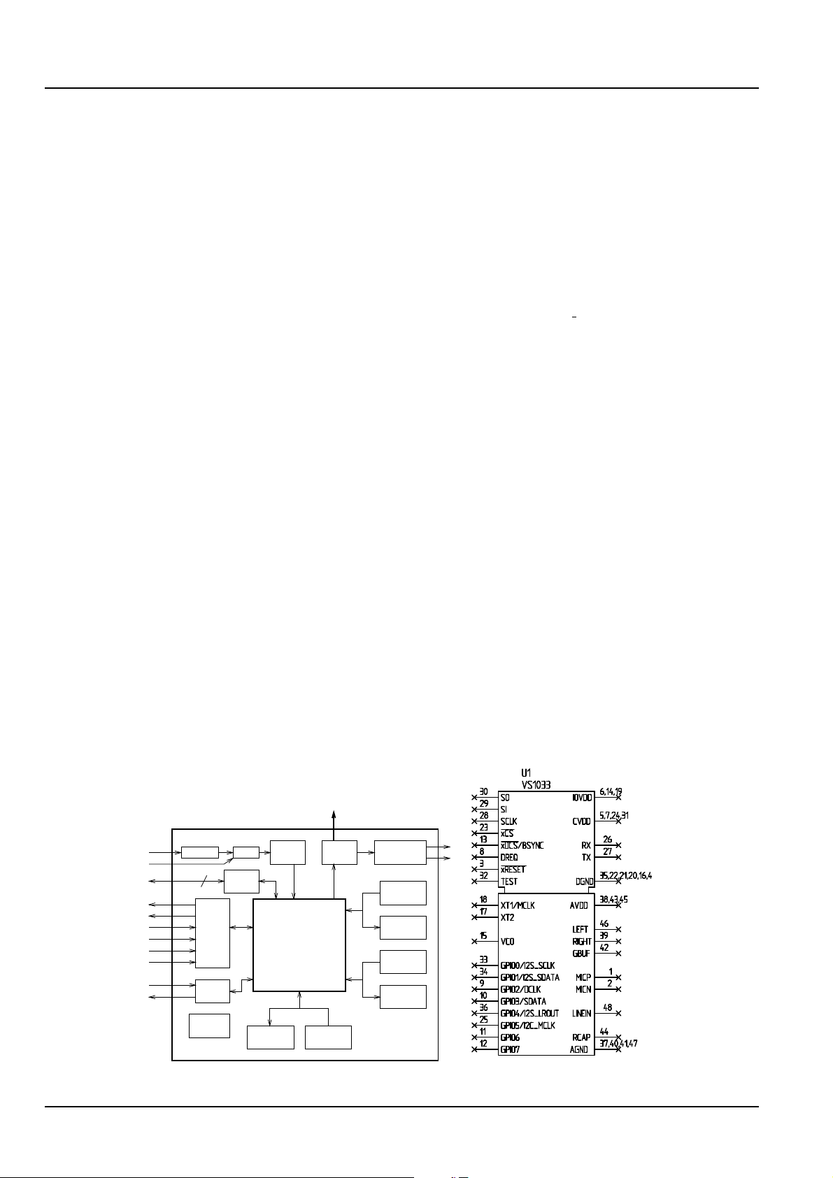
VSDSP
4
XDCS
MIC AMP
Clock
multiplier
MUX
line
audio
mic
audio
8
I2S
VS1033
VS1033 - MP3/AAC/WMA/MIDI
AUDIO CODEC
VS1033C
Features
• Decodes MPEG 1 & 2 audio layer III (CBR
+VBR +ABR); layers I & II optional;
MPEG4/2 AAC-LC-2.0.0.0 (+PNS);
WMA 4.0/4.1/7/8/9allprofiles (5-384 kbps);
WAV (PCM + IMA ADPCM);
General MIDI / SP-MIDI format 0 files
• Encodes IMA ADPCM from microphone
or line input
• Streaming support for MP3 and WAV
• EarSpeaker Spatial Processing
• Bass and treble controls
• Operates with a single clock 12..13 MHz
• Can also be used with 24..26 MHz clocks
• Internal PLL clock multiplier
• Low-power operation
• High-quality on-chip stereo DAC with no
phase error between channels
• Stereo earphone driver capable of driving a
30Ω load
• Quiet power-on and power-off
• I2S interface for external DAC
• Separate operating voltages for analog,
digital and I/O
• 5.5 KiB On-chip RAM for user code / data
• Serial control and data interfaces
• Can be used as a slave co-processor
• SPI flash boot for special applications
• UART for debugging purposes
• New functions may be added with software
and 8 GPIO pins
• Lead-free RoHS-compliantpackage(Green)
Description
VS1033 is a single-chip MP3/AAC/WMA/MIDI
audio decoder and ADPCM encoder. It contains
a high-performance, proprietary low-power DSP
processor core VS DSP4, working data memory,
5 KiB instruction RAM and 0.5 KiB data RAM
for user applications, serial control and input data
interfaces, upto 8 general purpose I/O pins, an
UART, as well as a high-quality variable-samplerate mono ADC and stereo DAC, followed by an
earphone amplifier and a common voltage buffer.
VS1033 receives its input bitstream through a serial input bus, which itlistenstoasasystemslave.
The input stream is decoded and passed through a
digital volume control to an 18-bit oversampling,
multi-bit, sigma-delta DAC. The decoding is controlled via a serial control bus. In addition to the
basic decoding, it is possible to add application
specific features,likeDSP effects, to theuserRAM
memory.
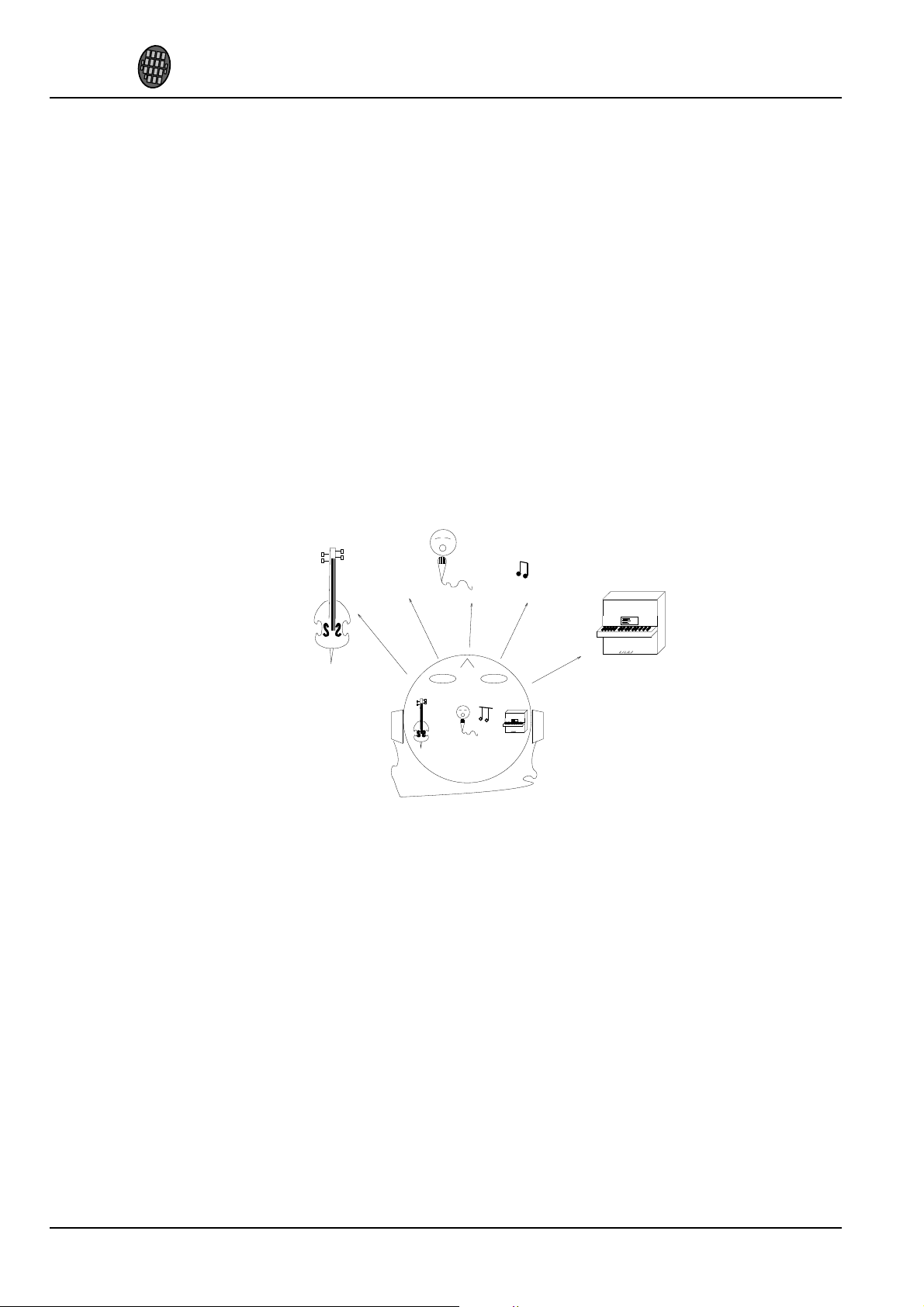
EarSpeaker spatial processing provides more natural sound in headphone listening conditions. It
widens the stereo image and positions the sound
sources outside the listener’s head.
Version 0.91, 2007-02-12 1
Page 2

VLSI
Solution
y
VS1033C
VS1033c PRELIMINARY
CONTENTS
Contents
1 Licenses 9
2 Disclaimer 9
3 Definitions 9
4 Characteristics & Specifications 10
4.1 Absolute Maximum Ratings . . . . . . . . . . . . . . . . . . . . . . . . . . . . . . . . 10
4.2 Recommended Operating Conditions . . . . . . . . . . . . . . . . . . . . . . . . . . . . 10
4.3 Analog Characteristics . . . . . . . . . . . . . . . . . . . . . . . . . . . . . . . . . . . 11
4.4 Power Consumption . . . . . . . . . . . . . . . . . . . . . . . . . . . . . . . . . . . . . 11
4.5 Digital Characteristics . . . . . . . . . . . . . . . . . . . . . . . . . . . . . . . . . . . 12
4.6 Switching Characteristics - Boot Initialization . . . . . . . . . . . . . . . . . . . . . . . 12
5 Packages and Pin Descriptions 13
5.1 Packages . . . . . . . . . . . . . . . . . . . . . . . . . . . . . . . . . . . . . . . . . . 13
5.1.1 LQFP-48 . . . . . . . . . . . . . . . . . . . . . . . . . . . . . . . . . . . . . . 13
5.1.2 BGA-49 . . . . . . . . . . . . . . . . . . . . . . . . . . . . . . . . . . . . . . . 13
5.2 LQFP-48 and BGA-49 Pin Descriptions . . . . . . . . . . . . . . . . . . . . . . . . . . 14
6 Connection Diagram, LQFP-48 16
7 SPI Buses 17
7.1 General . . . . . . . . . . . . . . . . . . . . . . . . . . . . . . . . . . . . . . . . . . . 17
Version 0.91, 2007-02-12 2
7.2 SPI Bus Pin Descriptions . . . . . . . . . . . . . . . . . . . . . . . . . . . . . . . . . . 17
7.2.1 VS1002 Native Modes (New Mode) . . . . . . . . . . . . . . . . . . . . . . . . 17
Page 3

VLSI
Solution
y
VS1033C
VS1033c PRELIMINARY
7.2.2 VS1001 Compatibility Mode . . . . . . . . . . . . . . . . . . . . . . . . . . . . 17
7.3 Data Request Pin DREQ . . . . . . . . . . . . . . . . . . . . . . . . . . . . . . . . . . 18
7.4 Serial Protocol for Serial Data Interface (SDI) . . . . . . . . . . . . . . . . . . . . . . . 18
7.4.1 General . . . . . . . . . . . . . . . . . . . . . . . . . . . . . . . . . . . . . . . 18
7.4.2 SDI in VS1002 Native Modes (New Mode) . . . . . . . . . . . . . . . . . . . . 18
7.4.3 SDI in VS1001 Compatibility Mode . . . . . . . . . . . . . . . . . . . . . . . . 19
7.4.4 Passive SDI Mode . . . . . . . . . . . . . . . . . . . . . . . . . . . . . . . . . 19
7.5 Serial Protocol for Serial Command Interface (SCI) . . . . . . . . . . . . . . . . . . . . 19
7.5.1 General . . . . . . . . . . . . . . . . . . . . . . . . . . . . . . . . . . . . . . . 19
CONTENTS
7.5.2 SCI Read . . . . . . . . . . . . . . . . . . . . . . . . . . . . . . . . . . . . . . 20
7.5.3 SCI Write . . . . . . . . . . . . . . . . . . . . . . . . . . . . . . . . . . . . . . 20
7.6 SPI Timing Diagram . . . . . . . . . . . . . . . . . . . . . . . . . . . . . . . . . . . . 21
7.7 SPI Examples with SM SDINEW and SM SDISHARED set . . . . . . . . . . . . . . . 22
7.7.1 Two SCI Writes . . . . . . . . . . . . . . . . . . . . . . . . . . . . . . . . . . . 22
7.7.2 Two SDI Bytes . . . . . . . . . . . . . . . . . . . . . . . . . . . . . . . . . . . 22
7.7.3 SCI Operation in Middle of Two SDI Bytes . . . . . . . . . . . . . . . . . . . . 23
8 Functional Description 24
8.1 Main Features . . . . . . . . . . . . . . . . . . . . . . . . . . . . . . . . . . . . . . . . 24
8.2 Supported Audio Codecs . . . . . . . . . . . . . . . . . . . . . . . . . . . . . . . . . . 24
8.2.1 Supported MP3 (MPEG layer III) Formats . . . . . . . . . . . . . . . . . . . . 24
Version 0.91, 2007-02-12 3
8.2.2 Supported MP1 (MPEG layer I) Formats . . . . . . . . . . . . . . . . . . . . . 25
8.2.3 Supported MP2 (MPEG layer II) Formats . . . . . . . . . . . . . . . . . . . . . 25
8.2.4 Supported AAC (ISO/IEC 13818-7) Formats . . . . . . . . . . . . . . . . . . . 26
8.2.5 Supported WMA Formats . . . . . . . . . . . . . . . . . . . . . . . . . . . . . 27
Page 4

VLSI
Solution
y
VS1033C
VS1033c PRELIMINARY
8.2.6 Supported RIFF WAV Formats . . . . . . . . . . . . . . . . . . . . . . . . . . . 28
8.2.7 Supported MIDI Formats . . . . . . . . . . . . . . . . . . . . . . . . . . . . . . 29
8.3 Data Flow of VS1033 . . . . . . . . . . . . . . . . . . . . . . . . . . . . . . . . . . . . 31
8.4 EarSpeaker Spatial Processing . . . . . . . . . . . . . . . . . . . . . . . . . . . . . . . 32
8.5 Serial Data Interface (SDI) . . . . . . . . . . . . . . . . . . . . . . . . . . . . . . . . . 33
8.6 Serial Control Interface (SCI) . . . . . . . . . . . . . . . . . . . . . . . . . . . . . . . . 34
8.7 SCI Registers . . . . . . . . . . . . . . . . . . . . . . . . . . . . . . . . . . . . . . . . 34
8.7.1 SCI MODE (RW) . . . . . . . . . . . . . . . . . . . . . . . . . . . . . . . . . 35
8.7.2 SCI STATUS (RW) . . . . . . . . . . . . . . . . . . . . . . . . . . . . . . . . . 37
CONTENTS
8.7.3 SCI BASS (RW) . . . . . . . . . . . . . . . . . . . . . . . . . . . . . . . . . . 37
8.7.4 SCI CLOCKF (RW) . . . . . . . . . . . . . . . . . . . . . . . . . . . . . . . . 38
8.7.5 SCI DECODE TIME (RW) . . . . . . . . . . . . . . . . . . . . . . . . . . . . 39
8.7.6 SCI AUDATA (RW) . . . . . . . . . . . . . . . . . . . . . . . . . . . . . . . . 39
8.7.7 SCI WRAM (RW) . . . . . . . . . . . . . . . . . . . . . . . . . . . . . . . . . 39
8.7.8 SCI WRAMADDR (W) . . . . . . . . . . . . . . . . . . . . . . . . . . . . . . 39
8.7.9 SCI HDAT0 and SCI HDAT1 (R) . . . . . . . . . . . . . . . . . . . . . . . . . 40
8.7.10 SCI AIADDR (RW) . . . . . . . . . . . . . . . . . . . . . . . . . . . . . . . . 41
8.7.11 SCI VOL (RW) . . . . . . . . . . . . . . . . . . . . . . . . . . . . . . . . . . . 41
8.7.12 SCI AICTRL[x] (RW) . . . . . . . . . . . . . . . . . . . . . . . . . . . . . . . 42
9 Operation 43
Version 0.91, 2007-02-12 4
9.1 Clocking . . . . . . . . . . . . . . . . . . . . . . . . . . . . . . . . . . . . . . . . . . . 43
9.2 Hardware Reset . . . . . . . . . . . . . . . . . . . . . . . . . . . . . . . . . . . . . . . 43
9.3 Software Reset . . . . . . . . . . . . . . . . . . . . . . . . . . . . . . . . . . . . . . . 43
9.4 ADPCM Recording . . . . . . . . . . . . . . . . . . . . . . . . . . . . . . . . . . . . . 45
Page 5

VLSI
Solution
y
VS1033C
VS1033c PRELIMINARY
9.4.1 Activating ADPCM mode . . . . . . . . . . . . . . . . . . . . . . . . . . . . . 45
9.4.2 Reading IMA ADPCM Data . . . . . . . . . . . . . . . . . . . . . . . . . . . . 45
9.4.3 Adding a RIFF Header . . . . . . . . . . . . . . . . . . . . . . . . . . . . . . . 46
9.4.4 Playing ADPCM Data . . . . . . . . . . . . . . . . . . . . . . . . . . . . . . . 47
9.4.5 Sample Rate Considerations . . . . . . . . . . . . . . . . . . . . . . . . . . . . 47
9.4.6 Example Code . . . . . . . . . . . . . . . . . . . . . . . . . . . . . . . . . . . 47
9.5 SPI Boot . . . . . . . . . . . . . . . . . . . . . . . . . . . . . . . . . . . . . . . . . . . 49
9.6 Play/Decode . . . . . . . . . . . . . . . . . . . . . . . . . . . . . . . . . . . . . . . . . 49
9.7 Feeding PCM data . . . . . . . . . . . . . . . . . . . . . . . . . . . . . . . . . . . . . 49
CONTENTS
9.8 Extra Parameters . . . . . . . . . . . . . . . . . . . . . . . . . . . . . . . . . . . . . . 50
9.8.1 Common Parameters . . . . . . . . . . . . . . . . . . . . . . . . . . . . . . . . 51
9.8.2 WMA . . . . . . . . . . . . . . . . . . . . . . . . . . . . . . . . . . . . . . . . 51
9.8.3 AAC . . . . . . . . . . . . . . . . . . . . . . . . . . . . . . . . . . . . . . . . 52
9.8.4 Midi . . . . . . . . . . . . . . . . . . . . . . . . . . . . . . . . . . . . . . . . . 52
9.9 Fast Forward / Rewind . . . . . . . . . . . . . . . . . . . . . . . . . . . . . . . . . . . 53
9.9.1 MP3 . . . . . . . . . . . . . . . . . . . . . . . . . . . . . . . . . . . . . . . . . 53
9.9.2 AAC - ADTS . . . . . . . . . . . . . . . . . . . . . . . . . . . . . . . . . . . . 53
9.9.3 AAC - ADIF, MP4 . . . . . . . . . . . . . . . . . . . . . . . . . . . . . . . . . 53
9.9.4 WMA . . . . . . . . . . . . . . . . . . . . . . . . . . . . . . . . . . . . . . . . 54
9.9.5 Midi . . . . . . . . . . . . . . . . . . . . . . . . . . . . . . . . . . . . . . . . . 54
9.10 SDI Tests . . . . . . . . . . . . . . . . . . . . . . . . . . . . . . . . . . . . . . . . . . 55
Version 0.91, 2007-02-12 5
9.10.1 Sine Test . . . . . . . . . . . . . . . . . . . . . . . . . . . . . . . . . . . . . . 55
9.10.2 Pin Test . . . . . . . . . . . . . . . . . . . . . . . . . . . . . . . . . . . . . . . 55
9.10.3 Memory Test . . . . . . . . . . . . . . . . . . . . . . . . . . . . . . . . . . . . 56
Page 6

VLSI
Solution
y
VS1033C
VS1033c PRELIMINARY
9.10.4 SCI Test . . . . . . . . . . . . . . . . . . . . . . . . . . . . . . . . . . . . . . . 56
10 VS1033 Registers 57
10.1 Who Needs to Read This Chapter . . . . . . . . . . . . . . . . . . . . . . . . . . . . . 57
10.2 The Processor Core . . . . . . . . . . . . . . . . . . . . . . . . . . . . . . . . . . . . . 57
10.3 VS1033 Memory Map . . . . . . . . . . . . . . . . . . . . . . . . . . . . . . . . . . . 57
10.4 SCI Registers . . . . . . . . . . . . . . . . . . . . . . . . . . . . . . . . . . . . . . . . 57
10.5 Serial Data Registers . . . . . . . . . . . . . . . . . . . . . . . . . . . . . . . . . . . . 57
10.6 DAC Registers . . . . . . . . . . . . . . . . . . . . . . . . . . . . . . . . . . . . . . . 58
CONTENTS
10.7 GPIO Registers . . . . . . . . . . . . . . . . . . . . . . . . . . . . . . . . . . . . . . . 59
10.8 Interrupt Registers . . . . . . . . . . . . . . . . . . . . . . . . . . . . . . . . . . . . . 60
10.9 A/D Modulator Registers . . . . . . . . . . . . . . . . . . . . . . . . . . . . . . . . . . 61
10.10Watchdog v1.0 2002-08-26 . . . . . . . . . . . . . . . . . . . . . . . . . . . . . . . . . . 62
10.10.1 Registers . . . . . . . . . . . . . . . . . . . . . . . . . . . . . . . . . . . . . . 62
10.11UART v1.1 2004-10-09 . . . . . . . . . . . . . . . . . . . . . . . . . . . . . . . . . . . 63
10.11.1 Registers . . . . . . . . . . . . . . . . . . . . . . . . . . . . . . . . . . . . . . 63
10.11.2 Status UARTx STATUS . . . . . . . . . . . . . . . . . . . . . . . . . . . . . . 63
10.11.3 Data UARTx DATA . . . . . . . . . . . . . . . . . . . . . . . . . . . . . . . . 64
10.11.4 Data High UARTx DATAH . . . . . . . . . . . . . . . . . . . . . . . . . . . . 64
10.11.5 Divider UARTx DIV . . . . . . . . . . . . . . . . . . . . . . . . . . . . . . . . 64
10.11.6 Interrupts and Operation . . . . . . . . . . . . . . . . . . . . . . . . . . . . . . 65
Version 0.91, 2007-02-12 6
10.12Timers v1.0 2002-04-23 . . . . . . . . . . . . . . . . . . . . . . . . . . . . . . . . . . . 66
10.12.1 Registers . . . . . . . . . . . . . . . . . . . . . . . . . . . . . . . . . . . . . . 66
10.12.2 Configuration TIMER CONFIG . . . . . . . . . . . . . . . . . . . . . . . . . . 66
10.12.3 Configuration TIMER ENABLE . . . . . . . . . . . . . . . . . . . . . . . . . . 67
Page 7

VLSI
Solution
y
VS1033C
VS1033c PRELIMINARY
10.12.4 Timer X Startvalue TIMER Tx[L/H] . . . . . . . . . . . . . . . . . . . . . . . 67
10.12.5 Timer X Counter TIMER TxCNT[L/H] . . . . . . . . . . . . . . . . . . . . . . 67
10.12.6 Interrupts . . . . . . . . . . . . . . . . . . . . . . . . . . . . . . . . . . . . . . 67
10.13I2S DAC Interface . . . . . . . . . . . . . . . . . . . . . . . . . . . . . . . . . . . . . 68
10.13.1 Registers . . . . . . . . . . . . . . . . . . . . . . . . . . . . . . . . . . . . . . 68
10.13.2 Configuration I2S CONFIG . . . . . . . . . . . . . . . . . . . . . . . . . . . . 68
10.14System Vector Tags . . . . . . . . . . . . . . . . . . . . . . . . . . . . . . . . . . . . . 69
10.14.1 AudioInt, 0x20 . . . . . . . . . . . . . . . . . . . . . . . . . . . . . . . . . . . 69
10.14.2 SciInt, 0x21 . . . . . . . . . . . . . . . . . . . . . . . . . . . . . . . . . . . . . 69
CONTENTS
10.14.3 DataInt, 0x22 . . . . . . . . . . . . . . . . . . . . . . . . . . . . . . . . . . . . 69
10.14.4 ModuInt, 0x23 . . . . . . . . . . . . . . . . . . . . . . . . . . . . . . . . . . . 69
10.14.5 TxInt, 0x24 . . . . . . . . . . . . . . . . . . . . . . . . . . . . . . . . . . . . . 70
10.14.6 RxInt, 0x25 . . . . . . . . . . . . . . . . . . . . . . . . . . . . . . . . . . . . . 70
10.14.7 Timer0Int, 0x26 . . . . . . . . . . . . . . . . . . . . . . . . . . . . . . . . . . 70
10.14.8 Timer1Int, 0x27 . . . . . . . . . . . . . . . . . . . . . . . . . . . . . . . . . . 70
10.14.9 UserCodec, 0x0 . . . . . . . . . . . . . . . . . . . . . . . . . . . . . . . . . . . 71
10.15System Vector Functions . . . . . . . . . . . . . . . . . . . . . . . . . . . . . . . . . . 71
10.15.1 WriteIRam(), 0x2 . . . . . . . . . . . . . . . . . . . . . . . . . . . . . . . . . . 71
10.15.2 ReadIRam(), 0x4 . . . . . . . . . . . . . . . . . . . . . . . . . . . . . . . . . . 71
10.15.3 DataBytes(), 0x6 . . . . . . . . . . . . . . . . . . . . . . . . . . . . . . . . . . 71
10.15.4 GetDataByte(), 0x8 . . . . . . . . . . . . . . . . . . . . . . . . . . . . . . . . . 72
11 Document VersionChanges 73
Version 0.91, 2007-02-12 7
10.15.5 GetDataWords(), 0xa . . . . . . . . . . . . . . . . . . . . . . . . . . . . . . . . 72
11.1 Version 0.91 for VS1033c, 2007-02-12 . . . . . . . . . . . . . . . . . . . . . . . . . . . 73
Page 8

VLSI
Solution
y
VS1033C
VS1033c PRELIMINARY
11.2 Version 0.9 for VS1033c, 2006-08-15 . . . . . . . . . . . . . . . . . . . . . . . . . . . 73
11.3 Version 0.8 for VS1033b, 2006-05-19 . . . . . . . . . . . . . . . . . . . . . . . . . . . 73
11.4 Version 0.6 for VS1033a, 2006-01-05 . . . . . . . . . . . . . . . . . . . . . . . . . . . 73
11.5 Version 0.5, 2005-10-21 . . . . . . . . . . . . . . . . . . . . . . . . . . . . . . . . . . 73
12 Contact Information 74
LIST OF FIGURES
List of Figures
1 Pin Configuration, LQFP-48. . . . . . . . . . . . . . . . . . . . . . . . . . . . . . . . . 13
2 Pin Configuration, BGA-49. . . . . . . . . . . . . . . . . . . . . . . . . . . . . . . . . 13
3 Typical Connection Diagram Using LQFP-48. . . . . . . . . . . . . . . . . . . . . . . . 16
4 BSYNC Signal - one byte transfer. . . . . . . . . . . . . . . . . . . . . . . . . . . . . . 19
5 BSYNC Signal - two byte transfer. . . . . . . . . . . . . . . . . . . . . . . . . . . . . . 19
6 SCI Word Read . . . . . . . . . . . . . . . . . . . . . . . . . . . . . . . . . . . . . . . 20
7 SCI Word Write . . . . . . . . . . . . . . . . . . . . . . . . . . . . . . . . . . . . . . . 20
8 SPI Timing Diagram. . . . . . . . . . . . . . . . . . . . . . . . . . . . . . . . . . . . . 21
9 Two SCI Operations. . . . . . . . . . . . . . . . . . . . . . . . . . . . . . . . . . . . . 22
10 Two SDI Bytes. . . . . . . . . . . . . . . . . . . . . . . . . . . . . . . . . . . . . . . . 22
11 Two SDI Bytes Separated By an SCI Operation. . . . . . . . . . . . . . . . . . . . . . . 23
12 Data Flow of VS1033. . . . . . . . . . . . . . . . . . . . . . . . . . . . . . . . . . . . 31
13 EarSpeaker externalized sound sources vs. normal inside-the-head sound . . . . . . . . . 32
Version 0.91, 2007-02-12 8
14 ADPCM Frequency Responses with 8kHz sample rate. . . . . . . . . . . . . . . . . . . 36
15 User’s Memory Map. . . . . . . . . . . . . . . . . . . . . . . . . . . . . . . . . . . . . 58
16 RS232 Serial Interface Protocol . . . . . . . . . . . . . . . . . . . . . . . . . . . . . . 63
17 I2S Interface, 192 kHz. . . . . . . . . . . . . . . . . . . . . . . . . . . . . . . . . . . . 68
Page 9

VLSI
Solution
y
VS1033C
VS1033c PRELIMINARY
1. LICENSES
1 Licenses
MPEG Layer-3 audio decoding technology licensed from Fraunhofer IIS and Thomson.
Note: if you enable Layer I and Layer II decoding, you are liable for any patent issues that may
arise from using these formats. Joint licensing of MPEG 1.0 / 2.0 Layer III does not cover all patents
pertaining to layers I and II.
VS1033 contains WMA decoding technology from Microsoft.
This product is protected by certain intellectual property rights of Microsoft and cannot be used
or further distributed without a license from Microsoft.
VS1033 contains AAC technology (ISO/IEC 13818-7) which cannot be used without a proper license
from Via Licensing Corporation or individual patent holders.
To the best of our knowledge, if the end product does not play a specific format that otherwise would
require a customer license: MPEG 1.0/2.0 layers I and II, WMA, or AAC, the respective license should
not be required. Decoding of MPEG layers I and II are disabled by default, and WMA and AAC format
exclusion can be easily performed based on the contents of the SCI HDAT1 register.
2 Disclaimer
This is a
preliminary
datasheet. All properties and figures are subject to change.
3 Definitions
B Byte, 8 bits.
b Bit.
Ki “Kibi” = 210= 1024 (IEC 60027-2).
Mi “Mebi” = 220= 1048576 (IEC 60027-2).
VS DSP VLSI Solution’s DSP core.
W Word. In VS DSP, instruction words are 32-bit and data words are 16-bit wide.
Version 0.91, 2007-02-12 9
Page 10
VLSI
Solution
y
VS1033c PRELIMINARY
4. CHARACTERISTICS&SPECIFICATIONS
4 Characteristics & Specifications
4.1 Absolute Maximum Ratings
Parameter Symbol Min Max Unit
Analog Positive Supply AVDD -0.3 3.6 V
Digital Positive Supply CVDD -0.3 2.7 V
I/O Positive Supply IOVDD -0.3 3.6 V
Current at Any Digital Output ±50 mA
Voltage at Any Digital Input -0.3 IOVDD+0.31V
Operating Temperature -40 +85
Storage Temperature -65 +150
1
Must not exceed 3.6 V
◦
◦
VS1033C
C
C
4.2 Recommended Operating Conditions
Parameter Symbol Min Typ Max Unit
Ambient Operating Temperature -40 +85◦C
Analog and Digital Ground
Positive Analog AVDD 2.5 2.8 3.6 V
Positive Digital CVDD 2.4 2.5 2.7 V
I/O Voltage IOVDD CVDD-0.6V 2.8 3.6 V
Input Clock Frequency
Internal Clock Frequency CLKI 12 36.864 55.3 MHz
Internal Clock Multiplier
Master Clock Duty Cycle 40 50 60 %
1
Must be connected together as close the device as possible for latch-up immunity.
2
The maximum sample rate that can be played with correct speed is XTALI/256.
Thus, XTALI must be at least 12.288 MHz to be able to play 48 kHz at correct speed.
3
Reset value is 1.0×. Recommended SC MULT=3.0×, SC ADD=1.0× (SCI CLOCKF=0x9000).
1
2
3
AGND DGND 0.0 V
XTALI 12 12.288 13 MHz
1.0× 3.0× 4.5×
Version 0.91, 2007-02-12 10
Page 11
VLSI
Solution
y
VS1033C
VS1033c PRELIMINARY
4. CHARACTERISTICS&SPECIFICATIONS
4.3 Analog Characteristics
Unless otherwisenoted: AVDD=2.5..2.85V, CVDD=2.4..2.7V, IOVDD=CVDD-0.6V..3.6V,TA=-40..+85◦C,
XTALI=12..13MHz, Internal Clock Multiplier 3.5×. DAC tested with 1307.894 Hz full-scale output
sinewave, measurement bandwidth 20..20000 Hz, analog output load: LEFT to GBUF 30Ω, RIGHT to
GBUF 30Ω. Microphone test amplitude 50 mVpp, fs=1 kHz, Line input test amplitude 1.1 V, fs=1 kHz.
Parameter Symbol Min Typ Max Unit
DAC Resolution 18 bits
Total Harmonic Distortion THD 0.1 0.3 %
Dynamic Range (DAC unmuted, A-weighted) IDR 90 dB
S/N Ratio (full scale signal) SNR 70 dB
Interchannel Isolation (Cross Talk) 50 75 dB
Interchannel Isolation (Cross Talk), with GBUF 40 dB
Interchannel Gain Mismatch -0.5 0.5 dB
Frequency Response -0.1 0.1 dB
Full Scale Output Voltage (Peak-to-peak) 1.3 1.5
Deviation from Linear Phase 5
Analog Output Load Resistance AOLR 16 30
Analog Output Load Capacitance 100 pF
Microphone input amplifier gain MICG 26 dB
Microphone input amplitude 50 1403mVpp AC
Microphone Total Harmonic Distortion MTHD 0.02 0.10 %
Microphone S/N Ratio MSNR 50 62 dB
Line input amplitude 2200 28003mVpp AC
Line input Total Harmonic Distortion LTHD 0.06 0.10 %
Line input S/N Ratio LSNR 60 68 dB
Line and Microphone input impedances 100 kΩ
1
2
1.7 Vpp
◦
Ω
1
3.0 volts can be achieved with +-to-+ wiring for mono difference sound.
2
AOLR may be much lower, but below Typical distortion performance may be compromised.
3
Above typical amplitude the Harmonic Distortion increases.
4.4 Power Consumption
Tested with an MPEG 1.0 Layer-3 128 kbps sample and generated sine. Output at full volume. Internal
clock multiplier 3.0×.
Parameter Min Typ Max Unit
Power Supply Consumption AVDD, Reset 0.6 5.0 µA
Power Supply Consumption CVDD = 2.5V, Reset 3.7 50.0 µA
Power Supply Consumption AVDD, sine test, 30Ω + GBUF 36.9 mA
Power Supply Consumption CVDD = 2.5V, sine test 8.2 mA
Power Supply Consumption AVDD, no load 7.0 mA
Power Supply Consumption AVDD, output load 30Ω 10.9 mA
Power Supply Consumption AVDD, 30Ω + GBUF 16.1 mA
Power Supply Consumption CVDD = 2.5V 14 mA
Version 0.91, 2007-02-12 11
Page 12
VLSI
Solution
y
VS1033C
VS1033c PRELIMINARY
4. CHARACTERISTICS&SPECIFICATIONS
4.5 Digital Characteristics
Parameter Symbol Min Typ Max Unit
High-Level Input Voltage 0.7×IOVDD IOVDD+0.31V
Low-Level Input Voltage -0.2 0.3×IOVDD V
High-Level Output Voltage at IO= -2.0 mA 0.7×IOVDD V
Low-Level Output Voltage at IO= 2.0 mA 0.3×IOVDD V
Input Leakage Current -1.0 1.0 µA
SPI Input Clock Frequency
2
CLK I
6
MHz
Rise time of all output pins, load = 50 pF 50 ns
1
Must not exceed 3.6V
2
Value for SCI reads. SCI and SDI writes allow
CLK I
4
.
4.6 Switching Characteristics - Boot Initialization
Parameter Symbol Min Max Unit
XRESET active time 2 XTALI
XRESET inactive to software ready 20000 500001XTALI
Power on reset, rise time to CVDD 10 V/s
1
DREQ rises when initialization is complete. You should not send any data or commands before that.
Version 0.91, 2007-02-12 12
Page 13
VLSI
Solution
y
VS1033C
1
48
A
B
C
D
E
F
G
1 2
3
4 5
6 7
TOP VIEW
0.80 TYP
4.80
7.00
1.10 REF
0.80 TYP
1.10 REF
4.80
7.00
A1 BALL PAD CORNER
VS1033c PRELIMINARY
5. PACKAGES AND PIN DESCRIPTIONS
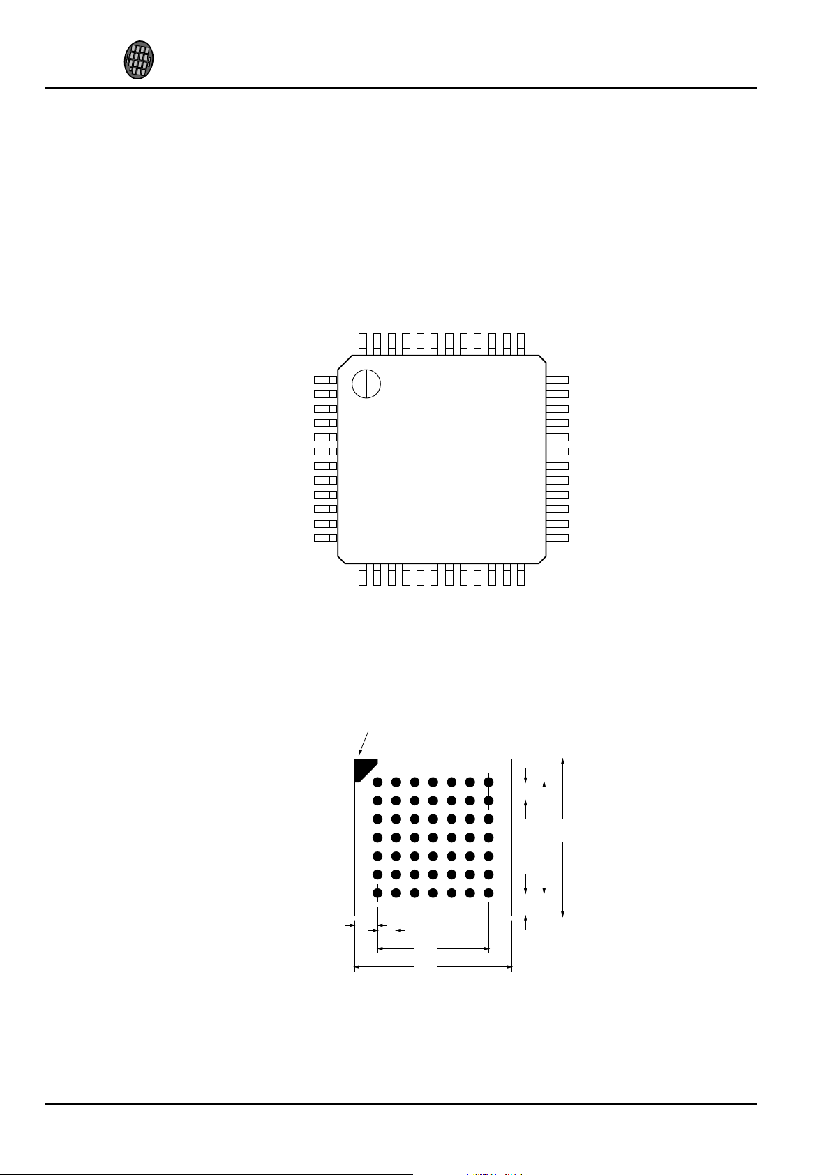
5 Packages and Pin Descriptions
5.1 Packages
Both LPQFP-48 and BGA-49 are lead (Pb) free and also RoHS compliant packages. RoHS is a short
name of Directive 2002/95/EC on the restriction of the use of certain hazardous substances in electrical
and electronic equipment.
5.1.1 LQFP-48
Figure 1: Pin Configuration, LQFP-48.
LQFP-48 package dimensions are at http://www.vlsi.fi/ .
5.1.2 BGA-49
BGA-49 package dimensions are at http://www.vlsi.fi/ .
Figure 2: Pin Configuration, BGA-49.
Version 0.91, 2007-02-12 13
Page 14

VLSI
Solution
y
VS1033c PRELIMINARY
5.2 LQFP-48 and BGA-49 Pin Descriptions
VS1033C
5. PACKAGES AND PIN DESCRIPTIONS
Pin Name LQFP
Pin
MICP 1 C3 AI Positive differential microphone input, self-biasing
MICN 2 C2 AI Negative differential microphone input, self-biasing
XRESET 3 B1 DI Active low asynchronous reset, schmitt-trigger input
DGND0 4 D2 DGND Core & I/O ground
CVDD0 5 C1 CPWR Core power supply
IOVDD0 6 D3 IOPWR I/O power supply
CVDD1 7 D1 CPWR Core power supply
DREQ 8 E2 DO Data request, input bus
GPIO2 / DCLK
GPIO3 / SDATA
GPIO6 11 F1 DIO General purpose IO 6
GPIO7 12 G1 DIO General purpose IO 7
XDCS / BSYNC
IOVDD1 14 F3 IOPWR I/O power supply
VCO 15 G2 DO For testing only (Clock VCO output)
DGND1 16 F4 DGND Core & I/O ground
XTALO 17 G3 AO Crystal output
XTALI 18 E4 AI Crystal input
IOVDD2 19 G4 IOPWR I/O power supply
IOVDD3 F5 IOPWR I/O power supply
DGND2 20 DGND Core & I/O ground
DGND3 21 G5 DGND Core & I/O ground
DGND4 22 F6 DGND Core & I/O ground
XCS 23 G6 DI Chip select input (active low)
CVDD2 24 G7 CPWR Core power supply
GPIO5 / I2S MCLK
RX 26 E6 DI UART receive, connect to IOVDD if not used
TX 27 F7 DO UART transmit
SCLK 28 D6 DI Clock for serial bus
SI 29 E7 DI Serial input
SO 30 D5 DO3 Serial output
CVDD3 31 D7 CPWR Core power supply
TEST 32 C6 DI Reserved for test, connect to IOVDD
GPIO0 / I2S SCLK
GPIO1 / I2S SDATA334 B6 DIO General purpose IO 1 / I2S SDATA
GND 35 B7 DGND I/O Ground
GPIO4 / I2S LROUT336 A7 DIO General purpose IO 4 / I2S LROUT
AGND0 37 C5 APWR Analog ground, low-noise reference
AVDD0 38 B5 APWR Analog power supply
RIGHT 39 A6 AO Right channel output
AGND1 40 B4 APWR Analog ground
AGND2 41 A5 APWR Analog ground
GBUF 42 C4 AO Common buffer for headphones, do NOT connect to
AVDD1 43 A4 APWR Analog power supply
RCAP 44 B3 AIO Filtering capacitance for reference
AVDD2 45 A3 APWR Analog power supply
LEFT 46 B2 AO Left channel output
AGND3 47 A2 APWR Analog ground
LINEIN 48 A1 AI Line input
1
1
1
9 E1 DIO General purpose IO 2 / serial input data bus clock
10 F2 DIO General purpose IO 3 / serial data input
13 E3 DI Data chip select / byte sync
3
25 E5 DIO General purpose IO 5 / I2S MCLK
3
33 C7 DIO General purpose IO 0 (SPIBOOT) / I2S SCLK
BGA
Ball
Pin
Type
Function
use 100 kΩ pull-down resistor
ground!
2
Version 0.91, 2007-02-12 14
Page 15
VLSI
Solution
y
VS1033c PRELIMINARY
1
First pin function is active in New Mode, latter in Compatibility Mode.
2
Unless pull-down resistor is used, SPI Boot is tried. See Chapter 9.5 for details.
3
If I2S CF ENA is ’0’ the pins are used for GPIO. See Chapter 10.13 for details.
5. PACKAGES AND PIN DESCRIPTIONS
Pin types:
VS1033C
Type Description
DI Digital input, CMOS Input Pad
DO Digital output, CMOS Input Pad
DIO Digital input/output
DO3 Digital output, CMOS Tri-stated OutputPad
AI Analog input
In BGA-49, D4 is a no-connect ball.
Type Description
AO Analog output
AIO Analog input/output
APWR Analog power supply pin
DGND Core or I/O ground pin
CPWR Core power supply pin
IOPWR I/O power supply pin
Version 0.91, 2007-02-12 15
Page 16
VLSI
Solution
y
VS1033c PRELIMINARY
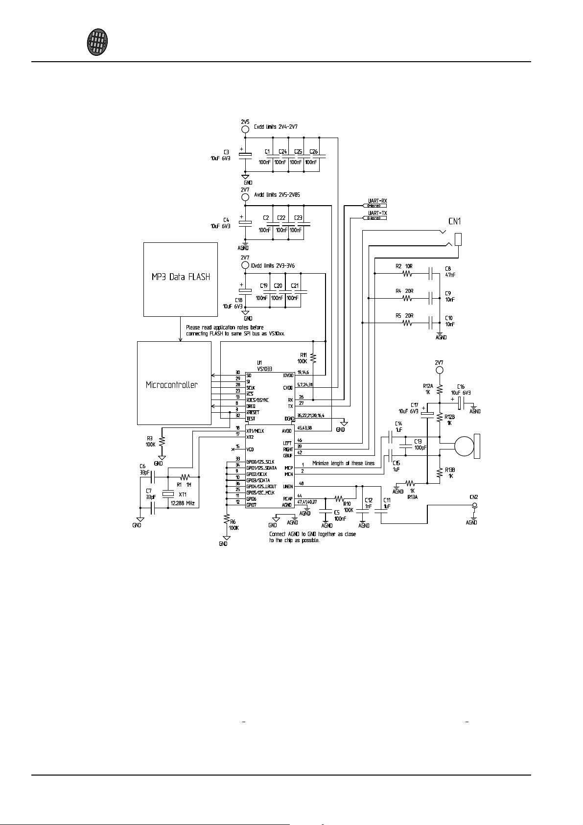
6 Connection Diagram, LQFP-48
VS1033C
6. CONNECTION DIAGRAM, LQFP-48
Figure 3: Typical Connection Diagram Using LQFP-48.
The common buffer GBUF can be used for common voltage (1.24 V) for earphones. This will eliminate
the need for large isolation capacitors on line outputs, and thus the audio output pins from VS1033 may
be connected directly to the earphone connector.
GBUF must NOT be connected to ground in any circumstance. If GBUF is not used, LEFT and RIGHT
must be provided with coupling capacitors. See application notes for details.
Unused GPIO pins should have a pull-down resistor.
If UART is not used, RX should be connected to IOVDD and TX be unconnected.
Do not connect any external load to XTALO.
Note: This connection assumes SM SDINEW is active (see Chapter 8.7.1). If also SM SDISHARE is
used, xDCS should be tied low or high (see Chapter 7.2.1).
Version 0.91, 2007-02-12 16
Page 17

VLSI
Solution
y
VS1033C
VS1033c PRELIMINARY
7. SPI BUSES
7 SPI Buses
7.1 General
The SPI Bus - that was originally used in some Motorola devices - has been used for both VS1033’s
Serial Data Interface SDI (Chapters 7.4 and 8.5) and Serial Control Interface SCI (Chapters 7.5 and 8.6).
7.2 SPI Bus Pin Descriptions
7.2.1 VS1002 Native Modes (New Mode)
These modes are active on VS1033 when SM SDINEW is set to 1 (default at startup). DCLK and
SDATA are not used for data transfer and they can be used as general-purpose I/O pins (GPIO2 and
GPIO3). BSYNC function changes to data interface chip select (XDCS).
SDI Pin SCI Pin Description
XDCS XCS Active low chip select input. A high level forces the serial interface into
standby mode, ending the current operation. A high level also forces serial
output (SO) to high impedance state. If SM SDISHARE is 1, pin
XDCS is not used, but the signal is generated internally by inverting
XCS.
SCK Serial clock input. The serial clock is also used internally as the master
clock for the register interface.
SCK can be gated or continuous. In either case, the first rising clock edge
after XCS has gone low marks the first bit to be written.
SI Serial input. If a chip select is active, SI is sampled on the rising CLK edge.
- SO Serial output. In reads, data is shifted out on the falling SCK edge.
In writes SO is at a high impedance state.
7.2.2 VS1001 Compatibility Mode
This mode is active when SM SDINEW is set to 0. In this mode, DCLK, SDATA and BSYNC are active.
SDI Pin SCI Pin Description
- XCS Active low chip select input. A high level forces the serial interface into
standby mode, ending the current operation. A high level also forces serial
output (SO) to high impedance state.
BSYNC - SDI data is synchronized with a rising edge of BSYNC.
DCLK SCK Serial clock input. The serial clock is also used internally as the master
SDATA SI Serial input. SI is sampled on the rising SCK edge, if XCS is low.
- SO Serial output. In reads, data is shifted out on the falling SCK edge.
clock for the register interface.
SCK can be gated or continuous. In either case, the first rising clock edge
after XCS has gone low marks the first bit to be written.
In writes SO is at a high impedance state.
Version 0.91, 2007-02-12 17
Page 18

VLSI
Solution
y
VS1033C
VS1033c PRELIMINARY
7. SPI BUSES
7.3 Data Request Pin DREQ
The DREQ pin/signal is used to signal if VS1033’s 2048-byte FIFO is capable of receiving data. If
DREQ is high, VS1033 can take at least 32 bytes of SDI data or one SCI command. DREQ is turned low
when the stream buffer is too full and for the duration of a SCI command.
Because of the 32-byte safety area, the sender may send upto 32 bytes of SDI data at a time without
checking the status of DREQ, making controlling VS1033 easier for low-speed microcontrollers.
Note: DREQ may turn low or high at any time, even during a byte transmission. Thus, DREQ should
only be used to decide whether to send more bytes. It does not need to abort a transmission that has
already started.
Note: In VS10XX products upto VS1002, DREQ was only used for SDI. In VS1003 and VS1033 DREQ
is also used to tell the status of SCI.
There are cases when you still want to send SCI commands when DREQ is low. Because DREQ is
shared between SDI and SCI, you can not determine if a SCI command has been executed if SDI is not
ready to receive. In this case you need a long enough delay after every SCI command to make certain
none of them is missed. The SCI Registers table in section 8.7 gives the worst-case handling time for
each SCI register write.
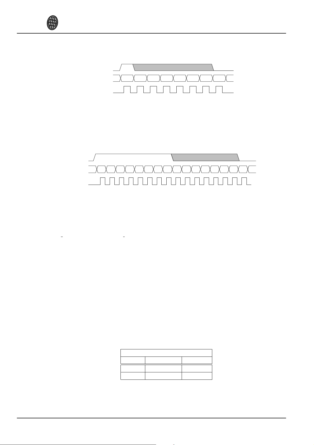
7.4 Serial Protocol for Serial Data Interface (SDI)
7.4.1 General
The serial data interface operates in slavemodesoDCLK signal must be generated by an externalcircuit.
Data (SDATA signal) can be clocked in at either the rising or falling edge of DCLK (Chapter 8.7).
VS1033 assumes its data input to be byte-sychronized. SDI bytes may be transmitted either MSb or LSb
first, depending of contents of SCI MODE (Chapter 8.7.1).
The firmware is able to accept the maximum bitrate the SDI supports.
7.4.2 SDI in VS1002 Native Modes (New Mode)
In VS1002native modes(SM NEWMODE is 1), byte synchronizationisachieved by XDCS.Thestateof
XDCS may not change while a data byte transfer is in progress. To always maintain data synchronization
even if there may be glitches in the boards using VS1033, it is recommended to turn XDCS every now
and then, for instance once after every flash data block or a few kilobytes, just to keep sure the host and
VS1033 are in sync.
If SM SDISHARE is 1, the XDCS signal is internally generated by inverting the XCS input.
For new designs, using VS1002 native modes are recommended.
Version 0.91, 2007-02-12 18
Page 19
VLSI
Solution
y
VS1033C
BSYNC
SDATA
DCLK
D7 D6 D5 D4 D3 D2 D1 D0
BSYNC
SDATA
DCLK
D7 D6 D5 D4 D3 D2 D1 D0
D7 D6 D5 D4 D3 D2 D1 D0
VS1033c PRELIMINARY
7. SPI BUSES
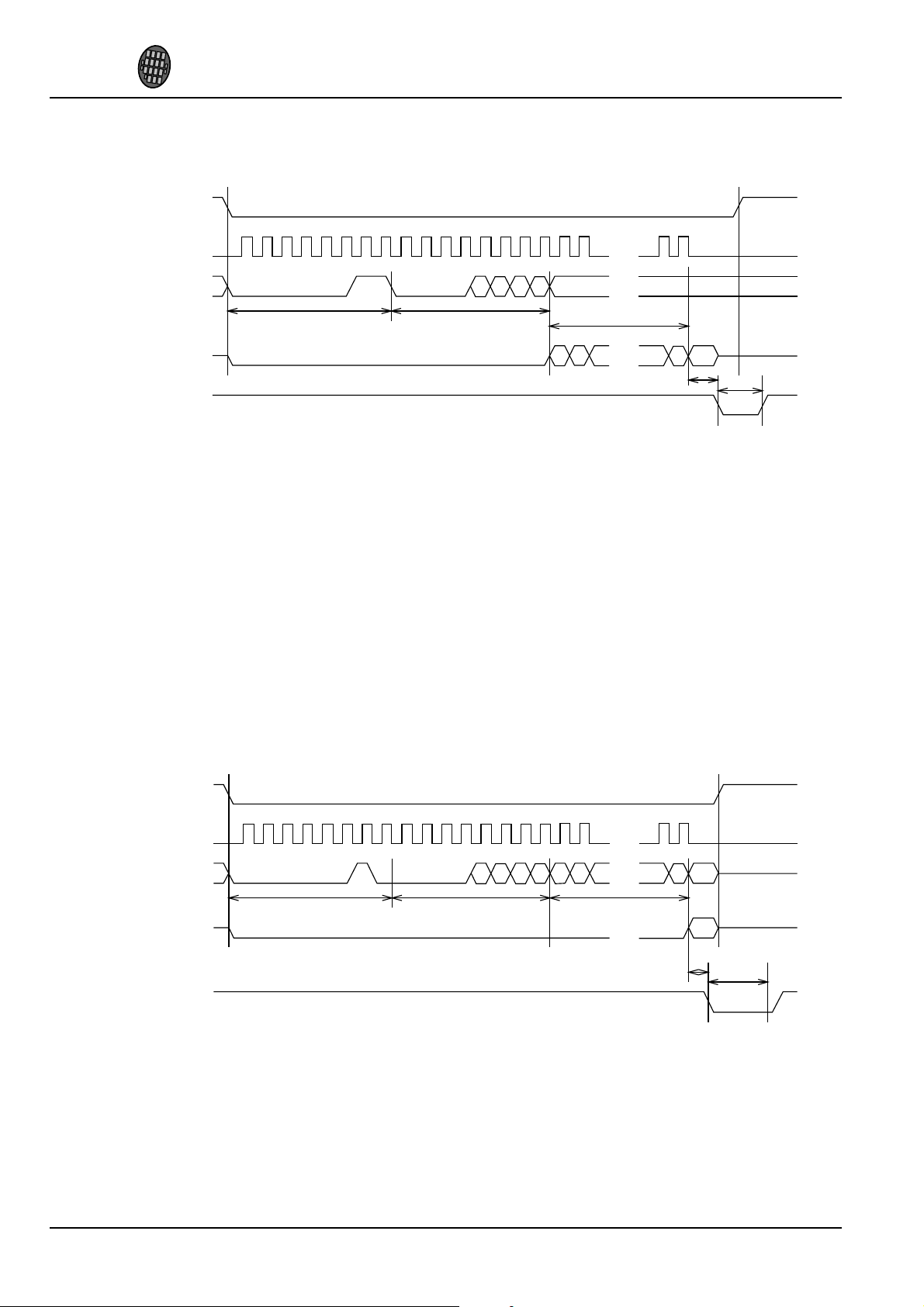
7.4.3 SDI in VS1001 Compatibility Mode
Figure 4: BSYNC Signal - one byte transfer.
When VS1033 is running in VS1001 compatibility mode, a BSYNC signal must be generated to ensure
correct bit-alignment of the input bitstream. The first DCLK sampling edge (rising or falling, depending
on selected polarity), during which the BSYNC is high, marks the first bit of a byte (LSB, if LSB-first
order is used, MSB, if MSB-first orderisused). If BSYNC is ’1’ when the last bit is received,thereceiver
stays active and next 8 bits are also received.
7.4.4 Passive SDI Mode
If SM NEWMODE is 0 and SM SDISHARE is 1, the operation is otherwise like the VS1001 compatibility mode, but bits are only received while the BSYNC signal is ’1’. Rising edge of BSYNC is still
used for synchronization.
7.5 Serial Protocol for Serial Command Interface (SCI)
7.5.1 General
The serial bus protocol for the Serial Command Interface SCI (Chapter 8.6) consists of an instruction
byte, address byte and one 16-bit data word. Each read or write operation can read or write a single
register. Data bits are read at the rising edge, so the user should update data at the falling edge. Bytes
are always send MSb first. XCS should be low for the full duration of the operation, but you can have
pauses between bits if needed.
The operation is specified by an 8-bit instruction opcode. The supported instructions are read and write.
See table below.
Figure 5: BSYNC Signal - two byte transfer.
Instruction
Name Opcode Operation
READ 0b0000 0011 Read data
WRITE 0b0000 0010 Write data
Note: VS1033 sets DREQ low after each SCI operation. The duration depends on the operation. It is not
allowed to start a new SCI/SDI operation before DREQ is high again.
Version 0.91, 2007-02-12 19
Page 20
VLSI
Solution
y
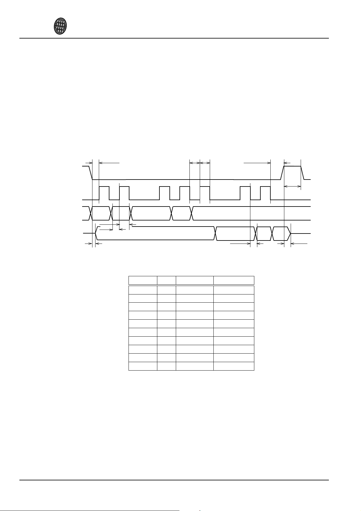
7.5.2 SCI Read
0 1 2 3 4 5 6 7 8 9 10 11 12 13 30 3114 15 16 17
0 0 0 0 0 0 1 1 0 0 0 0
3 2 1 0
0 0 0 0 0 0 0 0 0 0 0 0 0 0 0 0
15 14 1 0
X
instruction (read) address
data out
XCS
SCK
SI
SO
don’t care don’t care
DREQ
execution
0 1 2 3 4 5 6 7 8 9 10 11 12 13 30 3114 15 16 17
0 0 0 0 0 0 1 0 0 0 0
3 2 1 0
1 0
X
address
XCS
SCK
SI
15 14
data out
0 0 0 0 0 0 0 0 0 0 0 0 0 0 0 0SO
0 0 0 0
X
0
instruction (write)
DREQ
execution
VS1033c PRELIMINARY
Figure 6: SCI Word Read
VS1033C
7. SPI BUSES
VS1033 registers are read from using the following sequence, as shown in Figure 6. First, XCS line is
pulled low to select the device. Then the READ opcode (0x3) is transmitted via the SI line followed by
an 8-bit word address. After the address has been read in, any further data on SI is ignored by the chip.
The 16-bit data corresponding to the received address will be shifted out onto the SO line.
XCS should be driven high after data has been shifted out.
DREQ is driven low for a short while when in a read operation by the chip. This is a very short time and
doesn’t require special user attention.
7.5.3 SCI Write
Version 0.91, 2007-02-12 20
Figure 7: SCI Word Write
VS1033 registers are written from using the following sequence, as shown in Figure 7. First, XCS line
is pulled low to select the device. Then the WRITE opcode (0x2) is transmitted via the SI line followed
by an 8-bit word address.
Page 21
VLSI
Solution
y
VS1033C
XCS
SCK
SI
SO
0 1 1514 16
tXCSS
tXCSH
tWL tWH
tH
tSU
tV
tZ
tDIS
tXCS
30
31
VS1033c PRELIMINARY
7. SPI BUSES
After the word has been shifted in and the last clock has been sent, XCS should be pulled high to end the
WRITE sequence.
After the last bit has been sent, DREQ is driven low for the duration of the register update, marked “execution” in the figure. The time varies depending on the register and its contents (see table in Chapter 8.7
for details). If the maximum time is longer than what it takes from the microcontroller to feed the next
SCI command or SDI byte, it is not allowed to finish a new SCI/SDI operation before DREQ has risen
up again.
7.6 SPI Timing Diagram
Figure 8: SPI Timing Diagram.
Symbol Min Max Unit
tXCSS 5 ns
tSU -26 ns
tH 2 CLKI cycles
tZ 0 ns
tWL 2 CLKI cycles
tWH 2 CLKI cycles
tV 2 (+ 25ns1) CLKI cycles
tXCSH -26 ns
tXCS 2 CLKI cycles
tDIS 10 ns
1
25ns is when pin loaded with 100pF capacitance. The time is shorter with lower capacitance.
Note: As tWL and tWH, as well as tH require at least 2 clock cycles, the maximum speed for the SPI
bus that can easily be used is 1/6 of VS1033’s internal clock speed CLKI. Slightly higher speed can be
achieved with very careful timing tuning. For details, see Application Notes for VS10XX.
Note: Although the timing is derived from the internal clock CLKI, the system always starts up in 1.0×
mode, thus CLKI=XTALI.
Note: Negative numbers mean that the signal can change in different order from what is shown in the
diagram.
Version 0.91, 2007-02-12 21
Page 22
VLSI
Solution
y
VS1033c PRELIMINARY
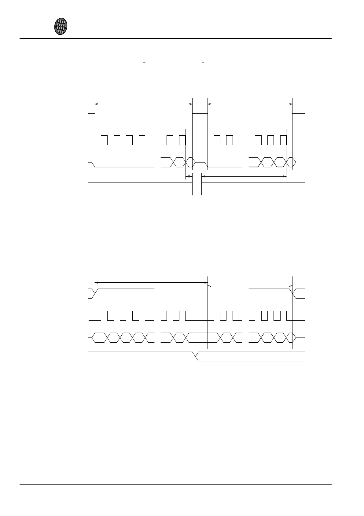
0
1 2 3 30 31
1 0 1 0
0 0 0 0 0 0
X X
XCS
SCK
SI
2
32 33 61 62 63
SCI Write 1
SCI Write 2
DREQ
DREQ up before finishing next SCI write
1 2 3
XCS
SCK
SI
7 6 5 4 3 1 0 7 6 5 2 1 0
X
SDI Byte 1
SDI Byte 2
0 6 7 8 9 13 14 15
DREQ
7.7 SPI Examples with SM SDINEW and SM SDISHARED set
7.7.1 Two SCI Writes
VS1033C
7. SPI BUSES
Figure 9: Two SCI Operations.
Figure 9 shows two consecutive SCI operations. Note that xCS must be raised to inactive state between
the writes. Also DREQ must be respected as shown in the figure.
7.7.2 Two SDI Bytes
Figure 10: Two SDI Bytes.
SDI data is synchronized with a raising edge of xCS as shown in Figure 10. However, every byte doesn’t
need separate synchronization.
Version 0.91, 2007-02-12 22
Page 23
VLSI
Solution
y
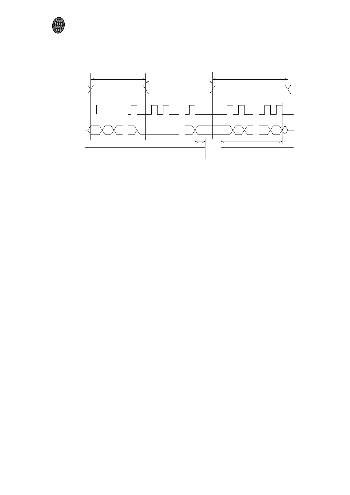
VS1033C
0
1
XCS
SCK
SI
7
7 6 5 1
0 0
0 7 6 5 1 0
SDI Byte
SCI Operation
SDI Byte
8 9 39 40 41 46 47
X
DREQ high before end of next transfer
VS1033c PRELIMINARY
7. SPI BUSES
7.7.3 SCI Operation in Middle of Two SDI Bytes
Figure 11: Two SDI Bytes Separated By an SCI Operation.
Figure 11 shows how an SCI operation is embedded in between SDI operations. xCS edges are used to
synchronize both SDI and SCI. Remember to respect DREQ as shown in the figure.
Version 0.91, 2007-02-12 23
Page 24
VLSI
Solution
y
VS1033C
VS1033c PRELIMINARY
8. FUNCTIONAL DESCRIPTION
8 Functional Description
8.1 Main Features
VS1033 is based on a proprietary digital signal processor, VS DSP. It contains all the code and data
memory needed for MP3, AAC, WMA and WAV PCM + ADPCM audio decoding, MIDI synthesizer,
together with serial interfaces, a multirate stereo audio DAC and analog output amplifiers and filters.
Also ADPCM audio encoding is supported using a microphone amplifier and A/D converter. A UART
is provided for debugging purposes.
8.2 Supported Audio Codecs
Conventions
Mark Description
+ Format is supported
- Format exists but is not supported
Format doesn’t exist
8.2.1 Supported MP3 (MPEG layer III) Formats
MPEG 1.01:
Samplerate / Hz Bitrate / kbit/s
32 40 48 56 64 80 96 112 128 160 192 224 256 320
48000 + + + + + + + + + + + + + +
44100 + + + + + + + + + + + + + +
32000 + + + + + + + + + + + + + +
MPEG 2.01:
Samplerate / Hz Bitrate / kbit/s
8 16 24 32 40 48 56 64 80 96 112 128 144 160
24000 + + + + + + + + + + + + + +
22050 + + + + + + + + + + + + + +
16000 + + + + + + + + + + + + + +
MPEG 2.51:
Samplerate / Hz Bitrate / kbit/s
8 16 24 32 40 48 56 64 80 96 112 128 144 160
12000 + + + + + + + + + + + + + +
11025 + + + + + + + + + + + + + +
8000 + + + + + + + + + + + + + +
1
Also all variable bitrate (VBR) formats are supported.
Version 0.91, 2007-02-12 24
Page 25
VLSI
Solution
y
VS1033c PRELIMINARY
8. FUNCTIONAL DESCRIPTION
8.2.2 Supported MP1 (MPEG layer I) Formats
Note: Layer I / II decoding must be specifically enabled from SCI MODE register.
MPEG 1.0:
Samplerate / Hz Bitrate / kbit/s
32 64 96 128 160 192 224 256 288 320 352 384 416 448
48000 + + + + + + + + + + + + + +
44100 + + + + + + + + + + + + + +
32000 + + + + + + + + + + + + + +
MPEG 2.0:
Samplerate / Hz Bitrate / kbit/s
32 48 56 64 80 96 112 128 144 160 176 192 224 256
24000 ? ? ? ? ? ? ? ? ? ? ? ? ? ?
22050 ? ? ? ? ? ? ? ? ? ? ? ? ? ?
16000 ? ? ? ? ? ? ? ? ? ? ? ? ? ?
VS1033C
8.2.3 Supported MP2 (MPEG layer II) Formats
Note: Layer I / II decoding must be specifically enabled from SCI MODE register.
MPEG 1.0:
Samplerate / Hz Bitrate / kbit/s
32 48 56 64 80 96 112 128 160 192 224 256 320 384
48000 + + + + + + + + + + + + + +
44100 + + + + + + + + + + + + + +
32000 + + + + + + + + + + + + + +
MPEG 2.0:
Samplerate / Hz Bitrate / kbit/s
8 16 24 32 40 48 56 64 80 96 112 128 144 160
24000 + + + + + + + + + + + + + +
22050 + + + + + + + + + + + + + +
16000 + + + + + + + + + + + + + +
Version 0.91, 2007-02-12 25
Page 26

VLSI
Solution
y
VS1033C
VS1033c PRELIMINARY
8. FUNCTIONAL DESCRIPTION
8.2.4 Supported AAC (ISO/IEC 13818-7) Formats
VS1033 decodes MPEG2-AAC-LC-2.0.0.0 and MPEG4-AAC-LC-2.0.0.0 streams. This means that the
low complexity profile with maximum of two channels can be decoded. If a stream contains more than
one element and/or element type, you can select which one to decode from the 16 single-channel, 16
channel-pair, and 16 low-frequency elements. The default is to select the first one that appears in the
stream.
Dynamic range control (DRC) is supported and can be controlled by the user to limit or enhance the
dynamic range of the material that has DRC information.
Both Sine window and Kaiser-Bessel-derived window are supported.
For MPEG4 pseudo-random noise substitution (PNS) is supported. Short frames (120 and 960 samples)
are not supported.
For AAC the streaming ADTS format is recommended. This format allows easy rewind and fast forward
because resynchronization is easily possible.
In addition to ADTS (.aac), MPEG2 ADIF (.aac) and MPEG4 AUDIO (.mp4 / .m4a) files are played,
but these formats are less suitable for rewind and fast forward operations. You can still implement these
features by using the safe jump points table and seek mechanism provided, or using slightly less robust
but much easier automatic resync mechanism (see Section 9.9).
Note: To be able to play the .mp4 and .m4a files, the mdat chunk must be the last chunk in the file.
AAC12:
Samplerate / Hz Maximum Bitrate kbit/s - for2 channels
≤96 132 144 192 264 288 384 529 576
48000 + + + + + + + + +
44100 + + + + + + + +
32000 + + + + + + +
24000 + + + + + +
22050 + + + + +
16000 + + + +
12000 + + +
11025 + +
8000 +
1
64000 Hz, 88200 Hz, and 96000 Hz AAC files are played but with wrong speed.
2
Version 0.91, 2007-02-12 26
Also all variable bitrate (VBR) formats are supported. Note that the table gives the maximum bitrate
allowed for two channels for a specific sample rate as defined by the AAC specification. The decoder
does not actually have a lower or upper limit.
Page 27

VLSI
Solution
y
VS1033C
VS1033c PRELIMINARY
8. FUNCTIONAL DESCRIPTION
8.2.5 Supported WMA Formats
Windows Media Audio codec versions 2, 7, 8, and 9 are supported. All WMA profiles (L1, L2, and L3)
are supported. Previously streams were separated into Classes 1, 2a, 2b, and 3. The decoder has passed
Microsoft’s conformance testing program.
WMA 4.0 / 4.1:
Samplerate Bitrate / kbit/s
/ Hz 5 6 8 10 12 16 20 22 32 40 48 64 80 96 128 160 192
8000 + + + +
11025 + +
16000 + + + +
22050 + + + +
32000 + + + + + +
44100 + + + + + + +
48000 + +
WMA 7:
Samplerate Bitrate / kbit/s
/ Hz 5 6 8 10 12 16 20 22 32 40 48 64 80 96 128 160 192
8000 + + + +
11025 + +
16000 + + + +
22050 + + + +
32000 + + + +
44100 + + + + + + + +
48000 + +
WMA 8:
Samplerate Bitrate / kbit/s
/ Hz 5 6 8 10 12 16 20 22 32 40 48 64 80 96 128 160 192
8000 + + + +
11025 + +
16000 + + + +
22050 + + + +
32000 + + + +
44100 + + + + + + + +
48000 + + +
WMA 9:
Samplerate Bitrate / kbit/s
/ Hz 5 6 8 10 12 16 20 22 32 40 48 64 80 96 128 160 192 256 320
8000 + + + +
11025 + +
16000 + + + +
22050 + + + +
32000 + + + +
44100 + + + + + + + + + + +
48000 + + + + +
In addition to these expected WMA decoding profiles, all other bitrate and samplerate combinations are
supported, including variable bitrate WMA streams. Note that WMA does not consume the bitstream as
evenly as MP3, so you need a higher peak transfer capability for clean playback at the same bitrate.
Version 0.91, 2007-02-12 27
Page 28

VLSI
Solution
y
VS1033c PRELIMINARY
8. FUNCTIONAL DESCRIPTION
8.2.6 Supported RIFF WAV Formats
The most common RIFF WAV subformats are supported.
Format Name Supported Comments
0x01 PCM + 16 and 8 bits, any sample rate ≤ 48kHz
0x02 ADPCM 0x03 IEEE FLOAT 0x06 ALAW 0x07 MULAW 0x10 OKI ADPCM 0x11 IMA ADPCM + Any sample rate ≤ 48kHz
0x15 DIGISTD 0x16 DIGIFIX 0x30 DOLBY AC2 0x31 GSM610 0x3b ROCKWELL ADPCM 0x3c ROCKWELL DIGITALK 0x40 G721 ADPCM 0x41 G728 CELP 0x50 MPEG 0x55 MPEGLAYER3 + For supportedMP3 modes, see Chapter 8.2.1
0x64 G726 ADPCM 0x65 G722 ADPCM -
VS1033C
Version 0.91, 2007-02-12 28
Page 29

VLSI
Solution
y
VS1033C
VS1033c PRELIMINARY
8.2.7 Supported MIDI Formats
General MIDI and SP-MIDI format 0 files are played. Format 1 and 2 files must be converted to format
0 by the user. The maximum simultaneous polyphony is 40. Actual polyphony depends on the internal
clock rate (which is user-selectable), the instruments used, whether the reverb effect is enabled, and the
possible global postprocessing effects enabled, such as bass and treble enhancers or EarSpeaker spatial
processing. The polyphony restriction algorithm makes use of the SP-MIDI MIP table, if present.
36.86 MHz (3.0× input clock) achieves 16-26 simultaneous sustained notes. The instantaneous amount
of notes can be larger. 36 MHz is a fair compromise between power consumption and quality, but higher
clocks can be used to increase the polyphony.
Reverb effect can be controlled by the user. In addition to reverb automatic and reverb off modes, 14
different decay times can be selected. These roughly correspond to different room sizes. Also, each
midi song decides how much effect each instrument gets. Because the reverb effect uses about 4 MHz of
processing power the automatic control enables reverb only when the internal clock is at least 3.0×.
8. FUNCTIONAL DESCRIPTION
When EarSpeaker spatial processing is active, MIDI reverb is not used.
New instruments have been implemented in addition to the 36 that are available in VS1003. VS1033c
now has unique instruments in the whole GM1 instrument set and one bank of GM2 percussions.
Version 0.91, 2007-02-12 29
Page 30

VLSI
Solution
y
VS1033C
VS1033c PRELIMINARY
VS1033c Melodic Instruments (GM1)
1 Acoustic Grand Piano 33 Acoustic Bass 65 Soprano Sax 97 Rain (FX 1)
2 Bright Acoustic Piano 34 Electric Bass (finger) 66 Alto Sax 98 Sound Track (FX 2)
3 Electric Grand Piano 35 Electric Bass (pick) 67 Tenor Sax 99 Crystal (FX 3)
4 Honky-tonk Piano 36 Fretless Bass 68 Baritone Sax 100 Atmosphere (FX 4)
5 Electric Piano 1 37 Slap Bass 1 69 Oboe 101 Brightness (FX 5)
6 Electric Piano 2 38 Slap Bass 2 70 English Horn 102 Goblins (FX 6)
7 Harpsichord 39 Synth Bass 1 71 Bassoon 103 Echoes (FX 7)
8 Clavi 40 Synth Bass 2 72 Clarinet 104 Sci-fi (FX 8)
9 Celesta 41 Violin 73 Piccolo 105 Sitar
10 Glockenspiel 42 Viola 74 Flute 106 Banjo
11 Music Box 43 Cello 75 Recorder 107 Shamisen
12 Vibraphone 44 Contrabass 76 Pan Flute 108 Koto
13 Marimba 45 Tremolo Strings 77 Blown Bottle 109 Kalimba
14 Xylophone 46 Pizzicato Strings 78 Shakuhachi 110 Bag Pipe
15 Tubular Bells 47 Orchestral Harp 79 Whistle 111 Fiddle
16 Dulcimer 48 Timpani 80 Ocarina 112 Shanai
17 Drawbar Organ 49 String Ensembles 1 81 Square Lead (Lead 1) 113 Tinkle Bell
18 Percussive Organ 50 String Ensembles 2 82 Saw Lead (Lead) 114 Agogo
19 Rock Organ 51 Synth Strings 1 83 Calliope Lead (Lead 3) 115 Pitched Percussion
20 Church Organ 52 Synth Strings 2 84 Chiff Lead (Lead 4) 116 Woodblock
21 Reed Organ 53 Choir Aahs 85 Charang Lead (Lead 5) 117 Taiko Drum
22 Accordion 54 Voice Oohs 86 Voice Lead (Lead 6) 118 Melodic Tom
23 Harmonica 55 Synth Voice 87 Fifths Lead (Lead 7) 119 Synth Drum
24 Tango Accordion 56 Orchestra Hit 88 Bass + Lead (Lead 8) 120 Reverse Cymbal
25 Acoustic Guitar (nylon) 57 Trumpet 89 New Age (Pad 1) 121 Guitar Fret Noise
26 Acoustic Guitar (steel) 58 Trombone 90 Warm Pad (Pad 2) 122 Breath Noise
27 Electric Guitar (jazz) 59 Tuba 91 Polysynth (Pad 3) 123 Seashore
28 Electric Guitar (clean) 60 Muted Trumpet 92 Choir (Pad 4) 124 Bird Tweet
29 Electric Guitar (muted) 61 French Horn 93 Bowed (Pad 5) 125 Telephone Ring
30 Overdriven Guitar 62 Brass Section 94 Metallic (Pad 6) 126 Helicopter
31 Distortion Guitar 63 Synth Brass 1 95 Halo (Pad 7) 127 Applause
32 Guitar Harmonics 64 Synth Brass 2 96 Sweep (Pad 8) 128 Gunshot
8. FUNCTIONAL DESCRIPTION
VS1033c Percussion Instruments (GM1+GM2)
27 High Q 43 High Floor Tom 59 Ride Cymbal 2 75 Claves
28 Slap 44 Pedal Hi-hat [EXC1] 60 High Bongo 76 Hi Wood Block
29 Scratch Push [EXC 7] 45 Low Tom 61 Low Bongo 77 Low Wood Block
30 Scratch Pull [EXC 7] 46 Open Hi-hat[EXC1] 62 Mute Hi Conga 78 Mute Cuica [EXC 4]
31 Sticks 47 Low-Mid Tom 63 Open Hi Conga 79 Open Cuica [EXC 4]
32 Square Click 48 High Mid Tom 64 Low Conga 80 Mute Triangle[EXC 5]
33 Metronome Click 49 Crash Cymbal 1 65 High Timbale 81 Open Triangle [EXC5]
34 Metronome Bell 50 High Tom 66 Low Timbale 82 Shaker
35 Acoustic Bass Drum 51 Ride Cymbal 1 67 High Agogo 83 Jingle bell
Version 0.91, 2007-02-12 30
36 Bass Drum 1 52 Chinese Cymbal 68 Low Agogo 84 Bell tree
37 Side Stick 53 Ride Bell 69 Cabasa 85 Castanets
38 Acoustic Snare 54 Tambourine 70 Maracas 86 Mute Surdo [EXC 6]
39 Hand Clap 55 Splash Cymbal 71 Short Whistle [EXC2] 87 Open Surdo [EXC 6]
40 Electric Snare 56 Cowbell 72 Long Whistle [EXC 2]
41 Low Floor Tom 57 Crash Cymbal 2 73 Short Guiro [EXC 3]
42 Closed Hi-hat [EXC1] 58 Vibra-slap 74 Long Guiro [EXC 3]
Page 31

VLSI
Solution
y
VS1033c PRELIMINARY
Volume
control
Audio
FIFO
S.rate.conv.
and DAC
R
Bitstream
FIFO
SDI
L
SCI_VOL
SM_ADPCM=0
2048 stereo
samples
Bass
enhancer
SB_AMPLITUDE=0
SB_AMPLITUDE!=0
AIADDR = 0
AIADDR != 0
User
Application
MP3
WAV/ADPCM/
WMA / AAC /
MIDI decode
ST_AMPLITUDE=0
ST_AMPLITUDE!=0
Treble
enhancer
Ear
Speaker
8.3 Data Flow of VS1033
VS1033C
8. FUNCTIONAL DESCRIPTION
Figure 12: Data Flow of VS1033.
First, depending on the audio data, and provided ADPCM encoding mode is not set, MP3, WMA, AAC,
PCM WAV, IMA ADPCM WAV, or MIDI data is received and decoded from the SDI bus.
After decoding, if SCI AIADDR is non-zero, application code is executed from the address pointed to
by that register. For more details, see Application Notes for VS10XX.
Then data may be sent to the Bass and Treble Enhancer depending on the SCI BASS register.
Next, headphone processing is performed, if the EarSpeaker spatial processing is active.
After that the signal is fed to the volume control unit, which also copies the data to the Audio FIFO.
The Audio FIFO holds the data, which is read by the Audio interrupt (Chapter 10.14.1) and fed to the
sample rate converter and DACs. The size of the audio FIFO is 2048 stereo (2×16-bit) samples, or 8
KiB.
The sample rate converter upsamples all different sample rates to XTALI/2, or 128 times the highest usable sample rate with 18-bit precision. This removes the need for complex PLL-based clocking schemes
and allows almost unlimited sample rate accuracy with one fixed input clock frequency. With a 12.288
MHz clock, the DA converter operates at 128 × 48 kHz, i.e. 6.144 MHz, and creates a stereo in-phase
analog signal. The oversampled output is low-pass filtered by an on-chip analog filter. This signal is then
forwarded to the earphone amplifier.
Version 0.91, 2007-02-12 31
Page 32
VLSI
Solution
y
VS1033C
VS1033c PRELIMINARY
8. FUNCTIONAL DESCRIPTION
8.4 EarSpeaker Spatial Processing
While listening to the headphones the sound has a tendency to be localized inside the head. The sound
field becomes flat and lacking the sensation of dimensions. This is unnatural, awkward and sometimes
even disturbing situation. This phenomenon is often referred in literature as ‘lateralization’, meaning
’in-the-head’ localization. Long-term listening to lateralized sound may lead to listening fatigue.
All real-life sound sources are external, leaving traces to the acoustic wavefront that arrives to the ear
drums. From these traces, the auditory system in the brain is able to judge the distance and angle of each
sound source. In loudspeaker listening the sound is external and these traces are available. In headphone
listening these traces are missing or ambiguous.
The EarSpeaker processing makes listening via headphones more like listening the same music from
real loudspeakers or live music. Once the EarSpeaker processing is activated, the instruments are moved
from inside to the outside of the head, making it easier to separate the different instruments (see figure
13). The listening experience becomes more natural and pleasant, and the stereo image is sharper as the
instruments are widely on front of the listener instead of being inside the head.
Figure 13: EarSpeaker externalized sound sources vs. normal inside-the-head sound
Note that EarSpeaker differs from any common spatial processing effects, such as echo, reverb, or bass
boost. EarSpeaker simulates accurately human auditory model and real listening environment acoustics.
Thus is does not change the tonal character of the music by introducing artificial effects.
EarSpeaker processing can be parameterized to a few different modes, each simulating a little different
type of acoustical situation and suiting for different personal preference and type of recording. See
section 8.7.1 for how to activate different modes.
Version 0.91, 2007-02-12 32
• Off: Best option when listening through loudspeakers or if the audio to be played contains binaural
preprocessing
• minimal: Suits well for listening to normal musical scores with headphones, very subtle
• normal: Suits well for listening to normal musical scores with headphones, moves sound source
farther than minimal
• extreme: Suits well for old or ’dry’ recordings, or if the audio to be played is artificial, for example
generated MIDI
Page 33

VLSI
Solution
y
VS1033C
VS1033c PRELIMINARY
8. FUNCTIONAL DESCRIPTION
8.5 Serial Data Interface (SDI)
The serial data interface is meant for transferring compressed MP3, WMA, or AAC data, WAV PCM and
ADPCM data as well as MIDI data.
If the input of the decoder is invalid or it is not received fast enough, analog outputs are automatically
muted.
Also several different tests may be activated through SDI as described in Chapter 9.
Version 0.91, 2007-02-12 33
Page 34

VLSI
Solution
y
VS1033C
VS1033c PRELIMINARY
8. FUNCTIONAL DESCRIPTION
8.6 Serial Control Interface (SCI)
The serial control interface is compatible with the SPI bus specification. Data transfers are always 16
bits. VS1033 is controlled by writing and reading the registers of the interface.
The main controls of the control interface are:
• control of the operation mode, clock, and builtin effects
• access to status information and header data
• access to encoded digital data
• uploading user programs
8.7 SCI Registers
VS1033 sets DREQ low when it detects an SCI operation and restores it when it has processed the
operation. The duration depends on the operation. If DREQ is low when an SCI operation is performed,
it also stays low after SCI operation processing.
If DREQ is high before a SCI operation, do not start a new SCI/SDI operation before DREQ is high
again. If DREQ is low before a SCI operation because the SDI can not accept more data, make certain
there is enough time to complete the operation before sending another.
SCI registers, prefix SCI
Reg Type Reset Time1Abbrev[bits] Description
0x0 rw 0x800 70 CLKI4MODE Mode control
0x1 rw 0x0C
3
40 CLKI STATUS Status of VS1033
0x2 rw 0 2100 CLKI BASS Built-in bass/treble enhancer
0x3 rw 0 11000 XTALI5CLOCKF Clock freq + multiplier
0x4 rw 0 40 CLKI DECODE TIME Decode time in seconds
0x5 rw 0 3200 CLKI AUDATA Misc. audio data
0x6 rw 0 80 CLKI WRAM RAM write/read
0x7 rw 0 80 CLKI WRAMADDR Base address for RAM write/read
0x8 r 0 - HDAT0 Stream header data 0
0x9 r 0 - HDAT1 Stream header data 1
0xA rw 0 3200 CLKI2AIADDR Start address of application
0xB rw 0 2100 CLKI VOL Volume control
0xC rw 0 50 CLKI2AICTRL0 Application control register 0
0xD rw 0 50 CLKI2AICTRL1 Application control register 1
0xE rw 0 50 CLKI2AICTRL2 Application control register 2
0xF rw 0 50 CLKI2AICTRL3 Application control register 3
1
This is the worst-case time that DREQ stays low after writing to this register. The user may choose to
skip the DREQ check for those register writes that take less than 100 clock cycles to execute.
2
In addition, the cycles spent in the user application routine must be counted.
3
Firmware changes the value of this register immediately to 0x58, and in less than 100 ms to 0x50.
4
When mode register write specifies a software reset the worst-case time is 20000 XTALI cycles.
5
Writing to this register may force internal clock to run at 1.0 × XTALI for a while. Thus it is not a
good idea to send SCI or SDI bits while this register update is in progress.
Version 0.91, 2007-02-12 34
Page 35
VLSI
Solution
y
VS1033C
VS1033c PRELIMINARY
8. FUNCTIONAL DESCRIPTION
8.7.1 SCI MODE (RW)
SCI MODE is used to control the operation of VS1033 and defaults to 0x0800 (SM SDINEW set).
Bit Name Function Value Description
0 SM DIFF Differential 0 normal in-phase audio
1 left channel inverted
1 SM LAYER12 Allow MPEG layers I & II 0 no
1 yes
2 SM RESET Soft reset 0 no reset
1 reset
3 SM OUTOFWAV Jump out of WAV decoding 0 no
1 yes
4 SM EARSPEAKER LO EarSpeaker low setting 0 off
1 active
5 SM TESTS Allow SDI tests 0 not allowed
1 allowed
6 SM STREAM Stream mode 0 no
1 yes
7 SM EARSPEAKER HI EarSpeaker high setting 0 off
1 active
8 SM DACT DCLK active edge 0 rising
1 falling
9 SM SDIORD SDI bit order 0 MSb first
1 MSb last
10 SM SDISHARE Share SPI chip select 0 no
1 yes
11 SM SDINEW VS1002 native SPI modes 0 no
1 yes
12 SM ADPCM ADPCM recording active 0 no
1 yes
13 SM ADPCM HP ADPCM high-pass filter active 0 no
1 yes
14 SM LINE IN ADPCM recording selector 0 microphone
1 line in
15 SM CLK RANGE Input clock range 0 12..13 MHz
1 24..26 MHz
When SM DIFF is set, the player inverts the left channel output. For a stereo input this creates virtual
surround, and for a mono input this creates a differential left/right signal.
SM LAYER12 enables MPEG 1.0 and 2.0 layer I and II decoding in addition to layer III. If you enable
Layer I and Layer II decoding, you are liable for any patent issues that may arise. Joint licensing
of MPEG 1.0 / 2.0 Layer III does not cover all patents pertaining to layers I and II.
Software reset is initiated by setting SM RESET to 1. This bit is cleared automatically.
If you want to stop decoding a WAV, WMA, or MIDI file in the middle, set SM OUTOFWAV, and send
data honouring DREQ until SM OUTOFWAV is cleared. SCI HDAT1 will also be cleared. For WMA
and MIDI it is safest to continue sending the stream, send zeroes for WAV.
Bits SM EARSPEAKER LO and SM EARSPEAKER HI control the EarSpeaker spatial processing. If
both are 0, the processing is not active. Other combinations activate the processing and select 3 different
effect levels: LO = 1, HI = 0 selects minimal, LO = 0, HI = 1 selects normal, and LO = 1, HI = 1 selects
extreme. EarSpeaker takes approximately 6 MIPS at 44.1 kHz sample rate. EarSpeaker is automatically
disabled with AAC files.
Version 0.91, 2007-02-12 35
Page 36
VLSI
Solution
y
VS1033C
0 500 1000 1500 2000 2500 3000 3500 4000
−20
−15
−10
−5
0
5
VS1023 AD Converter with and Without HP Filter
Frequency / Hz
Amplitude / dB
No High−Pass
High−Pass
VS1033c PRELIMINARY
8. FUNCTIONAL DESCRIPTION
If SM TESTS is set, SDI tests are allowed. For more details on SDI tests, look at Chapter 9.10.
SM STREAM activates VS1033’s stream mode. In this mode, data should be sent with as even intervals
as possible and preferable in blocks of less than 512 bytes, and VS1033 makes every attempt to keep its
input buffer half full by changing its playback speed upto 5%. For best quality sound, the average speed
error should be within 0.5%, the bitrate should not exceed 160 kbit/s and VBR should not be used. For
details, see Application Notes for VS10XX. This mode only works with MP3 and WAV files.
SM DACT defines the active edge of data clock for SDI. When ’0’, data is read at the rising edge, when
’1’, data is read at the falling edge.
When SM SDIORD is clear, bytes on SDI are sent MSb first. By setting SM SDIORD, the user may
reverse the bit order for SDI, i.e. bit 0 is received first and bit 7 last. Bytes are, however, still sent in the
default order. This register bit has no effect on the SCI bus.
Setting SM SDISHARE makes SCI and SDI share the same chip select, as explained in Chapter 7.2, if
also SM SDINEW is set.
Setting SM SDINEW will activateVS1002 native serial modes as described in Chapters 7.2.1 and 7.4.2.
Note, that this bit is set as a default when VS1033 is started up.
By activating SM ADPCM andSM RESET at the sametime,theuserwill activateIMAADPCMrecording mode (see section 9.4). If SM ADPCM HP is set (use only for 8 kHz sample rate), ADPCM mode
will start with a high-pass filter. This may help intelligibility of speech when there is lots of background
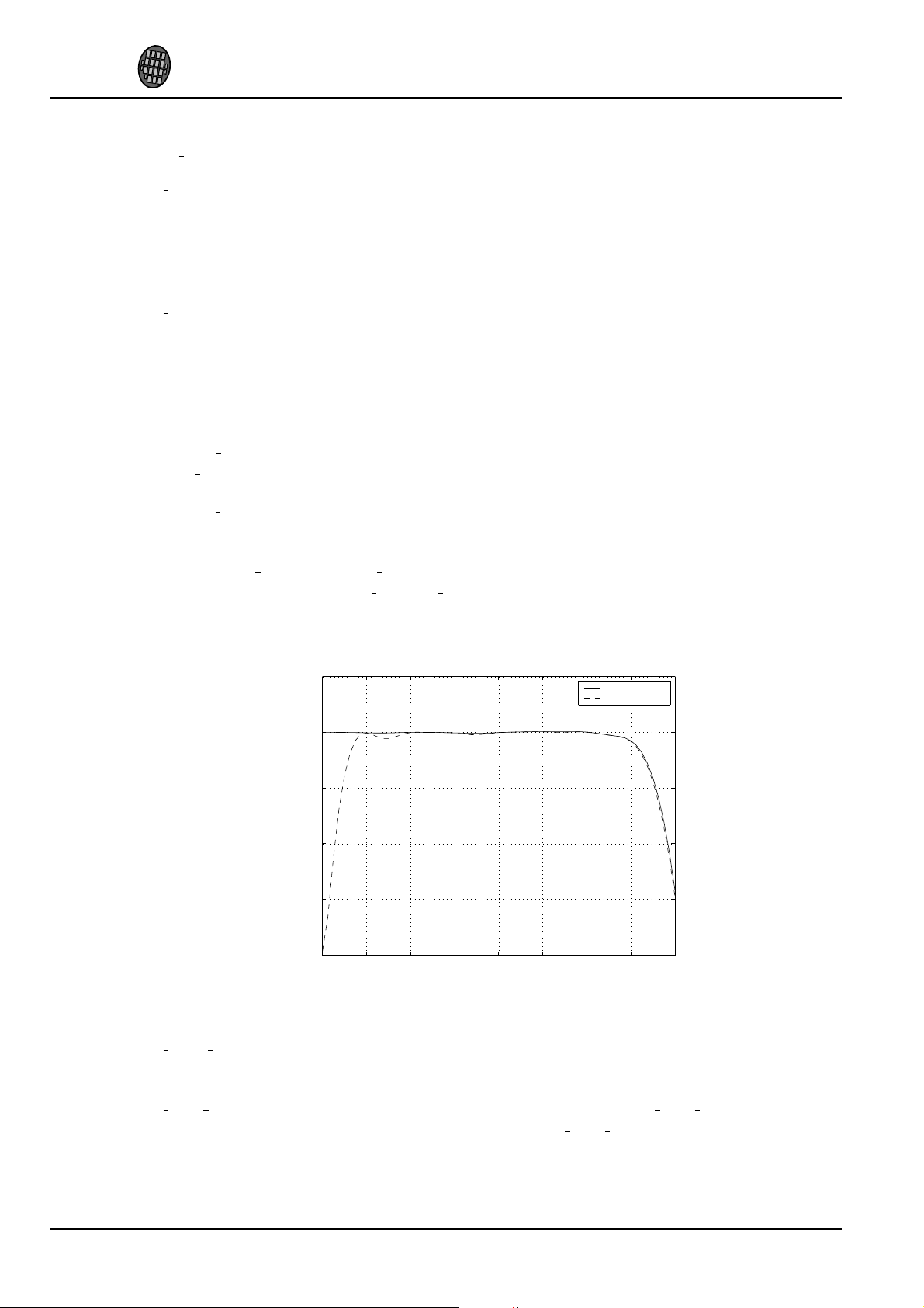
noise. The difference created to the ADPCM encoder frequency response is as shown in Figure 14.
Figure 14: ADPCM Frequency Responses with 8 kHz sample rate.
SM LINE IN is used to select the input for ADPCM recording. If ’0’, microphone input pins MICP and
MICN are used; if ’1’, LINEIN is used.
SM CLK RANGE activates a clock divider in the XTAL input. When SM CLK RANGE is set, from
the chip’s point of view e.g. 24 MHz becomes 12 MHz. SM CLK RANGE should be set as soon as
possible after a chip reset.
Version 0.91, 2007-02-12 36
Page 37
VLSI
Solution
y
VS1033C
VS1033c PRELIMINARY
8.7.2 SCI STATUS (RW)
SCI STATUS contains information on the current status of VS1033 and lets the user shutdown the chip
without audio glitches.
Name Bits Description
SS VER 6:4 Version
SS APDOWN2 3 Analog driver powerdown
SS APDOWN1 2 Analog internal powerdown
SS AVOL 1:0 Analog volume control
SS VER is 0 for VS1001, 1 for VS1011, 2 for VS1002, 3 for VS1003, and 5 for VS1033.
SS APDOWN2controlsanalog driverpowerdown. Normally thisbitis controlled by thesystemfirmware.
However, if the user wants to powerdown VS1033 with a minimum power-off transient, turn this bit to
1, then wait for at least a few milliseconds before activating reset.
8. FUNCTIONAL DESCRIPTION
SS APDOWN1 controls internal analog powerdown. This bit is meant to be used by the system firmware
only.
SS AVOL is the analog volume control: 0 = -0 dB, 1 = -6 dB, 3 = -12 dB. This register is meant to be
used automatically by the system firmware only. Use SCI VOL to control the analog powerdown.
8.7.3 SCI BASS (RW)
Name Bits Description
ST AMPLITUDE 15:12 Treble Control in 1.5 dB steps (-8..7, 0 = off)
ST FREQLIMIT 11:8 Lower limit frequency in 1000 Hz steps (1..15)
SB AMPLITUDE 7:4 Bass Enhancement in 1 dB steps (0..15, 0 = off)
SB FREQLIMIT 3:0 Lower limit frequency in 10 Hz steps (2..15)
The Bass Enhancer VSBE is a powerful bass boosting DSP algorithm, which tries to take the most out
of the users earphones without causing clipping.
VSBE is activated when SB AMPLITUDE is non-zero. SB AMPLITUDE should be set to the user’s
preferences, and SB FREQLIMIT to roughly 1.5 times the lowest frequency the user’s audio system can
reproduce. For example setting SCI BASS to 0x00f6 will have 15 dB enhancement below 60 Hz.
Note: Because VSBE tries to avoid clipping, it gives the best bass boost with dynamical music material,
or when the playback volume is not set to maximum. It also does not create bass: the source material
must have some bass to begin with.
Treble Control VSTC is activated when ST AMPLITUDE is non-zero. For example setting SCI BASS
to 0x7a00 will have 10.5 dB treble enhancement at and above 10 kHz.
Bass Enhancer uses about 2.1 MIPS and Treble Control 1.2 MIPS at 44100 Hz sample rate. Both can be
on simultaneously.
Version 0.91, 2007-02-12 37
Page 38
VLSI
Solution
y
VS1033C
VS1033c PRELIMINARY
8. FUNCTIONAL DESCRIPTION
8.7.4 SCI CLOCKF (RW)
The operation of SCI CLOCKF is different in VS1003 and VS1033 than in VS10x1 and VS1002. For
general applications with 12.288 MHz clock use 0x9000 for 3.0 × ..4.0×, or 0xa800 for 3.5 × ..4.0×.
SCI CLOCKF bits
Name Bits Description
SC MULT 15:13 Clock multiplier
SC ADD 12:11 Allowed multiplier addition
SC FREQ 10: 0 Clock frequency
SC MULT activates the built-in clock multiplier. This will multiply XTALI to create a higher CLKI.
The values are as follows:
SC MULT MASK CLKI
0 0x0000 XTALI
1 0x2000 XTALI×1.5
2 0x4000 XTALI×2.0
3 0x6000 XTALI×2.5
4 0x8000 XTALI×3.0
5 0xa000 XTALI×3.5
6 0xc000 XTALI×4.0
7 0xe000 XTALI×4.5
SC ADD tells, howmuchthe decoder firmware is allowedtoadd to the multiplier specified bySC MULT
if more cycles are temporarily needed to decode a WMA stream. The values are:
SC ADD MASK Multiplier addition
0 0x0000 No modification is allowed
1 0x0800 0.5×
2 0x1000 1.0×
3 0x1800 1.5×
SC FREQ is used to tell if the input clock XTALI is running at something else than 12.288 MHz. XTALI
is set in 4 kHz steps. The formula for calculating the correct value for this register is
XT ALI−8000000
4000
(XTALI is in Hz).
Note: The default value 0 is assumed to mean XTALI=12.288 MHz.
Note: because maximum sample rate is
XT ALI
256
, all sample rates are not available if XTALI < 12.288
MHz.
Note: Automatic clock change can only happen when decoding WMA files. Automatic clock change is
done one 0.5× at a time. This does not cause a drop to 1.0× clock and you can use the same SCI and
SDI clock throughout the WMA file.
Example: If SCI CLOCKF is 0x9BE8, SC MULT = 4, SC ADD = 3 and SC FREQ = 0x3E8 = 1000.
This means thatXTALI = 1000×4000+8000000 = 12 MHz. The clock multiplier issetto3.0×XTALI=
36 MHz, and the maximum allowed multiplier that the firmware may automatically choose to use is
(3.0 + 1.5)×XTALI = 54 MHz.
Version 0.91, 2007-02-12 38
Page 39

VLSI
Solution
y
VS1033C
VS1033c PRELIMINARY
8.7.5 SCI DECODE TIME (RW)
When decoding correct data, current decoded time is shown in this register in full seconds.
The user may change the value of this register. In that case the new value should be written twice.
SCI DECODE TIME is reset atevery softwareresetandalso when WAV (PCM or IMA ADPCM), AAC,
WMA, or MIDI decoding starts or ends.
8.7.6 SCI AUDATA (RW)
When decoding correct data, the current sample rate and number of channels can be found in bits 15:1
and 0 of SCI AUDATA, respectively. Bits 15:1 contain the sample rate divided by two, and bit 0 is 0 for
mono data and 1 for stereo. Writing to SCI AUDATA will change the sample rate directly.
Example: 44100 Hz stereo data reads as 0xAC45 (44101).
Example: 11025 Hz mono data reads as 0x2B10 (11024).
Example: Writing 0xAC80 sets sample rate to 44160Hz, stereo mode does not change.
8. FUNCTIONAL DESCRIPTION
To reduce the digital power consumption when in idle, you can write a low samplerate to SCI AUDATA.
8.7.7 SCI WRAM (RW)
SCI WRAM is used to upload application programs and data to instruction and data RAMs. The start
address must be initialized by writing to SCI WRAMADDR prior to the first write/read of SCI WRAM.
As 16 bits of data can be transferred with one SCI WRAM write/read, and the instruction word is 32 bits
long, twoconsecutive writes/reads areneededforeach instruction word. The byte orderisbig-endian(i.e.
most significant words first). After each full-word write/read, the internal pointer is autoincremented.
8.7.8 SCI WRAMADDR (W)
SCI WRAMADDR is used to set the program address for following SCI WRAM writes/reads. Address
offset of 0 is used for X, 0x4000 for Y, and 0x8000 for instruction memory. Peripheral registers can also
be accessed.
SM WRAMADDR Dest. addr. Bits/ Description
Start.. .End Start.. .End Word
0x1800.. .0x187F 0x1800...0x187F 16 X data RAM
0x5800.. .0x587F 0x1800...0x187F 16 Y data RAM
0x8030.. .0x84FF 0x0030...0x04FF 32 Instruction RAM
0xC000.. .0xFFFF 0xC000...0xFFFF 16 I/O
Only user areas in X, Y, and instruction memory are listed above. Other areas can be accessed, but should
not be written to unless otherwise specified.
Version 0.91, 2007-02-12 39
Page 40

VLSI
Solution
y
VS1033C
VS1033c PRELIMINARY
8. FUNCTIONAL DESCRIPTION
8.7.9 SCI HDAT0 and SCI HDAT1 (R)
For WAV files, SCI HDAT1 contains 0x7665 (“ve”). SCI HDAT0 contains the data rate in double word
increments for all supported RIFF WAVE formats: mono and stereo 8-bit or 16-bit PCM, mono and
stereo IMA ADPCM. To get the byte rate of the file, multiply the value by 4. To get the bit rate of the
file, multiply the value by 32. Note: usage of SCI HDAT0 with WAV files has changed from VS1003.
For AAC ADTS streams, SCI HDAT1 contains 0x4154 (“AT”). For AAC ADIF files, SCI HDAT1 contains 0x4144 (“AD”). For AAC .mp4 / .m4a files, SCI HDAT1 contains 0x4D34 (“M4”). SCI HDAT0
contains the average data rate in bytes per second. To get the bit rate of the file, multiply the value by 8.
For WMA files, SCI HDAT1 contains 0x574D(“WM”)andSCI HDAT0 contains the data rate measured
in bytes per second. To get the bit rate of the file, multiply the value by 8.
for MIDI files, SCI HDAT1 contains 0x4D54 (“MT”) and SCI HDAT0 contains the average data rate in
bytes per second. To get the bit rate of the file, multiply the value by 8. Note: usage of SCI HDAT0 with
MIDI has changed from VS1003.
For MP3 files, SCI HDAT1 is between 0xFFE0 and 0xFFFF. SCI HDAT1 / 0 contain the following:
Bit Function Value Explanation
HDAT1[15:5] syncword 2047 stream valid
HDAT1[4:3] ID 3 ISO 11172-3 MPG 1.0
2 ISO 13818-3 MPG 2.0 (1/2-rate)
1 MPG 2.5 (1/4-rate)
0 MPG 2.5 (1/4-rate)
HDAT1[2:1] layer 3 I
2 II
1 III
0 reserved
HDAT1[0] protect bit 1 No CRC
0 CRC protected
HDAT0[15:12] bitrate see bitrate table
HDAT0[11:10] sample rate 3 reserved
2 32/16/ 8 kHz
1 48/24/12 kHz
0 44/22/11 kHz
HDAT0[9] pad bit 1 additional slot
0 normal frame
HDAT0[8] private bit not defined
HDAT0[7:6] mode 3 mono
2 dual channel
1 joint stereo
0 stereo
HDAT0[5:4] extension see ISO 11172-3
HDAT0[3] copyright 1 copyrighted
0 free
HDAT0[2] original 1 original
0 copy
HDAT0[1:0] emphasis 3 CCITT J.17
2 reserved
1 50/15 microsec
0 none
Version 0.91, 2007-02-12 40
Page 41

VLSI
Solution
y
VS1033C
VS1033c PRELIMINARY
When read, SCI HDAT0 and SCI HDAT1 contain header information that is extracted from MP3 stream
currently being decoded. After reset both registers are cleared, indicating no data has been found yet.
The “sample rate” field in SCI HDAT0 is interpreted according to the following table:
“sample rate” ID=3 ID=2 ID=0,1
3 - - 2 32000 16000 8000
1 48000 24000 12000
0 44100 22050 11025
The “bitrate” field in HDAT0 is read according to the following table. Notice that for variable bitrate
stream the value changes constantly.
Layer I Layer II Layer III
“bitrate” ID=3 ID=0,1,2 ID=3 ID=0,1,2 ID=3 ID=0,1,2
kbit/s kbit/s kbit/s
15 forbidden forbidden forbidden forbidden forbidden forbidden
14 448 256 384 160 320 160
13 416 224 320 144 256 144
12 384 192 256 128 224 128
11 352 176 224 112 192 112
10 320 160 192 96 160 96
9 288 144 160 80 128 80
8 256 128 128 64 112 64
7 224 112 112 56 96 56
6 192 96 96 48 80 48
5 160 80 80 40 64 40
4 128 64 64 32 56 32
3 96 56 56 24 48 24
2 64 48 48 16 40 16
1 32 32 32 8 32 8
0 - - - - - -
8. FUNCTIONAL DESCRIPTION
8.7.10 SCI AIADDR (RW)
SCI AIADDR indicates the start address of the application code written earlier with SCI WRAMADDR
and SCI WRAM registers. If no application code is used, this register should not be initialized, or it
should be initialized to zero. For more details, see Application Notes for VS10XX.
Version 0.91, 2007-02-12 41
8.7.11 SCI VOL (RW)
SCI VOL is a volume control for the player hardware. The most significant byte of the volume register
controls the left channel volume, the low part controls the right channel volume. The channel volume
Page 42

VLSI
Solution
y
VS1033C
VS1033c PRELIMINARY
sets the attenuation from the maximum volume level in 0.5 dB steps. Thus, maximum volume is 0x0000
and total silence is 0xFEFE.
Note, that after hardware reset the volume is set to full volume. Resetting the software does not reset the
volume setting.
Setting SCI VOL to 0xFFFF will activate analog powerdown mode.
Example: for a volume of -2.0 dB for the left channel and -3.5dB for the right channel: (2.0/0.5) = 4,
3.5/0.5 = 7 → SCI VOL = 0x0407.
Example: SCI VOL = 0x2424 → both left and right volumes are 0x24 * -0.5 = -18.0 dB
8.7.12 SCI AICTRL[x] (RW)
8. FUNCTIONAL DESCRIPTION
SCI AICTRL[x] registers ( x=[0 .. 3] ) can be used to access the user’s application program.
Version 0.91, 2007-02-12 42
Page 43

VLSI
Solution
y
VS1033C
VS1033c PRELIMINARY
9. OPERATION
9 Operation
9.1 Clocking
VS1033 operates on a single, nominally 12.288 MHz fundamental frequency master clock. This clock
can begeneratedbyexternal circuitry (connectedtopinXTALI)orby the internal clock chrystal interface
(pins XTALI and XTALO).
VS1033 can also use 24..26 MHz clocks when SM CLK RANGE is set to 1. From the chip’s point of
view the input clock is then 12..13 MHz.
9.2 Hardware Reset
When the XRESET -signal is driven low, VS1033 is reset and all the control registers and internal states
are set to the initial values. XRESET-signal is asynchronous to any external clock. The reset mode
doubles as a full-powerdown mode, where both digital and analog parts of VS1033 are in minimum
power consumption stage, and where clocks are stopped. Also XTALO is grounded.
When XRESET is asseted, all output pins go to their default states. All input pins will go to highimpedance state (to input state), except SO, which is still controlled by the XCS.
After a hardware reset (or at power-up) DREQ will stay down for around 20000 clock cycles, which
means an approximate 1.6 ms delay if VS1033 is run at 12.288 MHz. After this the user should set
such basic software registers as SCI MODE, SCI BASS, SCI CLOCKF, and SCI VOL before starting
decoding. See section 8.7 for details.
If the input clock is 24..26 MHz, SM CLK RANGE should be set as soon as possible after a chip reset
without waiting for DREQ.
Internal clock can be multiplied with a PLL. Supported multipliers through the SCI CLOCKF register
are 1.0 × . . . 4.5× the input clock. Reset value for Internal Clock Multiplier is 1.0×. If typical values
are wanted, the Internal Clock Multiplier needs to be set to 3.0× after reset. Wait until DREQ rises, then
write value 0x9800 to SCI CLOCKF (register 3). See section 8.7.4 for details.
9.3 Software Reset
In some cases the decoder software hastobereset. This is done by activating bit 2 in SCI MODE register
(Chapter 8.7.1). Then wait for at least 2 µs, then look at DREQ. DREQ will stay down for at least 20000
clock cycles, which means an approximate 1.6 ms delay if VS1033 is run at 12.288 MHz. After DREQ
is up, you may continue playback as usual.
If you want to make sure VS1033 doesn’t cut the ending of low-bitrate data streams and you want to do
a software reset, it is recommended to feed 2048 zeros (honoring DREQ) to the SDI bus after the file and
before the reset. This is especially important for MIDI files.
If youwantto interrupt the playingofaWAV,AAC, WMA,orMIDIfile in the middle, setSM OUTOFWAV
Version 0.91, 2007-02-12 43
Page 44

VLSI
Solution
y
VS1033C
VS1033c PRELIMINARY
in themoderegister, and senddatahonouring DREQ (with athree-secondtimeout)until SM OUTOFWAV
is cleared (SCI HDAT1 will also be cleared) before continuing with a software reset. For WMA and
MIDI it is safest to continue sending the stream, send zeroes for WAV. MP3 can be interrupted without
SM OUTOFWAV by just sending zero bytes, because it is a stream format.
9. OPERATION
Version 0.91, 2007-02-12 44
Page 45

VLSI
Solution
y
VS1033C
VS1033c PRELIMINARY
9. OPERATION
9.4 ADPCM Recording
This chapter explains how to create RIFF/WAV file with IMA ADPCM format. This is a widely supported ADPCM format and many PC audio playback programs can play it. IMA ADPCM recording
gives roughly a compression ratio of 4:1 compared to linear, 16-bit audio. This makes it possible to
record 8 kHz audio at 32.44 kbit/s.
9.4.1 Activating ADPCM mode
IMA ADPCM recording mode is activated by setting bits SM RESET and SM ADPCM in SCI MODE.
Optionally a high-pass-filter can be enabled for 8kHzsamplerateby also setting SM ADPCM HP at the
same time. Line input is used instead of mic if SM LINE IN is set. Before activatingADPCMrecording,
user must write a clock divider value to SCI AICTRL0 and gain to SCI AICTRL1.
The differences of using SM ADPCM HP are presented in figure 14 (page 36). As a general rule, audio
will be fuller and closer to original if SM ADPCM HP is not used. However, speech may be more
intelligible with the high-pass filter active. Use the filter only with 8kHz sample rate.
Before activating ADPCM recording, user should write a clock divider value to SCI AICTRL0. The
F
sampling frequency is calculated from the following formula: f
s
=
c
, where Fcis the internal clock
256×d
(CLKI) and d is the divider value in SCI AICTRL0. The lowest valid value for d is 4. If SCI AICTRL0
contains 0, the default divider value 12 is used.
Examples:
F
= 2.0 × 12.288 MHz, d = 12. Now f
c
F
= 2.5 × 14.745 MHz, d = 18. Now f
c
F
= 2.5 × 13 MHz, d = 16. Now f
c
=
s
2.0×12288000
=
s
s
2.5×13000000
256×12
2.5×14745000
=
256×18
256×16
= 8000 Hz.
= 8000 Hz.
= 7935 Hz.
Also, before activating ADPCM mode, the user has to set linear recording gain control to register
SCI AICTRL1. 1024 is equal to digital gain 1, 512 is equal to digital gain 0.5 and so on. If the user
wants to use automatic gain control (AGC), SCI AICTRL1 should be set to 0. Typical speech applications usually are better off using AGC, as this takes care of relatively uniform speech loudness in
recordings.
Since VS1033c SCI AICTRL2 controls the maximum AGC gain. If SCI AICTRL2 is zero, the maximum gain is 65535 (64×), i.e. whole range is used. This is compatible with previous operation.
9.4.2 Reading IMA ADPCM Data
After IMA ADPCM recording has been activated, registers SCI HDAT0 and SCI HDAT1 have new
functions.
The IMA ADPCM sample buffer is 1024 16-bit words. The fill status of the buffer can be read from
Version 0.91, 2007-02-12 45
SCI HDAT1. If SCI HDAT1 is greater than 0, you can read as many 16-bit words from SCI HDAT0. If
the data is not read fast enough, the buffer overflows and returns to empty state.
Note: if SCI HDAT1 ≥ 896, it may be better to wait for the buffer to overflow and clear before reading
samples. That way you may avoid buffer aliasing.
Page 46

VLSI
Solution
y
VS1033C
VS1033c PRELIMINARY
9. OPERATION
Each IMA ADPCM block is 128 words, i.e. 256 bytes. If you wish to interrupt reading data and possibly
continue later, please stop at a 128-word boundary. This way whole blocks are skipped and the encoded
stream stays valid.
9.4.3 Adding a RIFF Header
To make your IMA ADPCM file a RIFF / WAV file, you have to add a header before the actual data.
Note that 2- and 4-byte values are little-endian (lowest byte first) in this format:
File Offset Field Name Size Bytes Description
0 ChunkID 4 "RIFF"
4 ChunkSize 4 F0 F1 F2 F3 File size - 8
8 Format 4 "WAVE"
12 SubChunk1ID 4 "fmt "
16 SubChunk1Size 4 0x14 0x0 0x0 0x0 20
20 AudioFormat 2 0x11 0x0 0x11 for IMA ADPCM
22 NumOfChannels 2 0x1 0x0 Mono sound
24 SampleRate 4 R0 R1 R2 R3 0x1f40 for 8 kHz
28 ByteRate 4 B0 B1 B2 B3 0xfd7 for 8 kHz
32 BlockAlign 2 0x0 0x1 0x100
34 BitsPerSample 2 0x4 0x0 4-bit ADPCM
36 ByteExtraData 2 0x2 0x0 2
38 ExtraData 2 0xf9 0x1 Samples per block (505)
40 SubChunk2ID 4 "fact"
44 SubChunk2Size 4 0x4 0x0 0x0 0x0 4
48 NumOfSamples 4 S0 S1 S2 S3
52 SubChunk3ID 4 "data"
56 SubChunk3Size 4 D0 D1 D2 D3 Data size (File Size-60)
60 Block1 256 First ADPCM block
316 .. . More ADPCM data blocks
If we have n audio blocks, the values in the table are as follows:
F = n × 256 + 52
R = F
B =
(see Chapter 9.4.1 to see how to calculate Fs)
s
Fs×256
505
S = n × 505. D = n × 256
If you know beforehand how much you are going to record, you may fill in the complete header before
any actual data. However, if you don’t know how much you are going to record, you have to fill in the
header size datas F , S and D after finishing recording.
The 128 words (256 bytes) of an ADPCM block are read from SCI HDAT0 and written into file as
follows. The high 8 bits of SCI HDAT0 should be written as the first byte to a file, then the low 8 bits.
Note that this is contrary to the default operation of some 16-bit microcontrollers, and you may have to
take extra care to do this right.
A way to see if you have written the file in the right way is to check bytes 2 and 3 (the first byte counts
as byte 0) of each 256-byte block. Byte 3 should always be zero.
Version 0.91, 2007-02-12 46
Page 47

VLSI
Solution
y
VS1033C
VS1033c PRELIMINARY
9. OPERATION
9.4.4 Playing ADPCM Data
In order to play back your IMA ADPCM recordings, you have to have a file with a header as described
in Chapter 9.4.3. If this is the case, all you need to do is to provide the ADPCM file through SDI as you
would with any audio file.
9.4.5 Sample Rate Considerations
VS10xx chips that support IMA ADPCM playback are capable of playing back ADPCM files with
any sample rate. However, some other programs may expect IMA ADPCM files to have some exact
sample rates, like 8000 or 11025Hz. Also, some programs or systems do not support sample rates below
8000Hz.
However, if you don’t have an appropriate clock, you may not be able to get an exact 8kHz sample rate.
If you have a 12 MHz clock, the closest sample rate you can get with 2.0 × 12 MHz and d = 12 is
f
= 7812.5Hz. Because the frequency error is only 2.4%, it may be best to set fs= 8000Hz to the
s
header if the same file is also to be played back with an PC. This causes the sample to be played back a
little faster (one minute is played in 59 seconds).
Note, however, that unless absolutely necessary, sample rates should not be tweaked in the way described
here.
If you want better quality with the expense of increased data rate, you can use higher sample rates, for
example 16 kHz.
9.4.6 Example Code
The following code initializes IMA ADPCM encoding on VS1003b/VS1023 and shows how to read the
data.
const unsigned char header[] = {
0x52, 0x49, 0x46, 0x46, 0x1c, 0x10, 0x00, 0x00,
0x57, 0x41, 0x56, 0x45, 0x66, 0x6d, 0x74, 0x20, /*|RIFF....WAVEfmt |*/
0x14, 0x00, 0x00, 0x00, 0x11, 0x00, 0x01, 0x00,
0x40, 0x1f, 0x00, 0x00, 0x75, 0x12, 0x00, 0x00, /*|........@......|*/
0x00, 0x01, 0x04, 0x00, 0x02, 0x00, 0xf9, 0x01,
0x66, 0x61, 0x63, 0x74, 0x04, 0x00, 0x00, 0x00, /*|.......fact....|*/
0x5c, 0x1f, 0x00, 0x00, 0x64, 0x61, 0x74, 0x61,
0xe8, 0x0f, 0x00, 0x00
};
unsigned char db[512]; /* data buffer for saving to disk */
Version 0.91, 2007-02-12 47
Page 48

VLSI
Solution
y
VS1033c PRELIMINARY
void RecordAdpcm1003(void) { /* VS1003b/VS1033c */
u_int16 w = 0, idx = 0;
... /* Check and locate free space on disk */
SetMp3Vol(0x1414); /* Recording monitor volume */
WriteMp3SpiReg(SCI_BASS, 0); /* Bass/treble disabled */
WriteMp3SpiReg(SCI_CLOCKF, 0x4430); /* 2.0x 12.288MHz */
Wait(100);
WriteMp3SpiReg(SCI_AICTRL0, 12); /* Div -> 12=8kHz 8=12kHz 6=16kHz */
Wait(100);
WriteMp3SpiReg(SCI_AICTRL1, 0); /* Auto gain */
Wait(100);
if (line_in) {
WriteMp3SpiReg(SCI_MODE, 0x5804); /* Normal SW reset + other bits */
} else {
WriteMp3SpiReg(SCI_MODE, 0x1804); /* Normal SW reset + other bits */
}
for (idx=0; idx < sizeof(header); idx++) { /* Save header first */
db[idx] = header[idx];
}
/* Fix rate if needed */
/*db[24] = rate;*/
/*db[25] = rate>>8;*/
9. OPERATION
VS1033C
/* Record loop */
while (recording_on) {
do {
w = ReadMp3SpiReg(SCI_HDAT1);
} while (w < 256 || w >= 896); /* wait until 512 bytes available */
while (idx < 512) {
w = ReadMp3SpiReg(SCI_HDAT0);
db[idx++] = w>>8;
db[idx++] = w&0xFF;
}
idx = 0;
write_block(datasector++, db); /* Write output block to disk */
}
... /* Fix WAV header information */
... /* Then update FAT information */
ResetMP3(); /* Normal reset, restore default settings */
SetMp3Vol(vol);
}
Version 0.91, 2007-02-12 48
Page 49

VLSI
Solution
y
VS1033C
VS1033c PRELIMINARY
9. OPERATION
9.5 SPI Boot
If GPIO0 is set with a pull-up resistor to 1 at boot time, VS1033 tries to boot from external SPI memory.
SPI boot redefines the following pins:
Normal Mode SPI Boot Mode
GPIO0 xCS
GPIO1 CLK
DREQ MOSI
GPIO2 MISO
The memory has to be an SPI Bus Serial EEPROM with 16-bit addresses (i.e. at least 1 KiB). The serial
speed used by VS1033 is 245 kHz with the nominal 12.288 MHz clock. The first three bytes in the
memory have to be 0x50, 0x26, 0x48.
9.6 Play/Decode
This is the normal operation mode of VS1033. SDI data is decoded. Decoded samples are converted to
analog domain by the internal DAC. If no decodable data is found, SCI HDAT0 and SCI HDAT1 are set
to 0 and analog outputs are muted.
When there is no input for decoding, VS1033 goes into idle mode (lower power consumption than during
decoding) and actively monitors the serial data input for valid data.
All different formats can be played back-to-back without software reset in-between. Send at least 2052
zeros after each stream. However, using software reset between streams may still be a good idea, as it
guards againstbrokenfiles. In this case you shouldtwaitfor the completion of the decoding (SCI HDAT1
and SCI HDAT0 become zero) before issuing software reset.
9.7 Feeding PCM data
VS1033 can be used as a PCM decoder by sending a WAV file header. If the length sent in the WAV
header is 0 or 0xFFFFFFF, VS1033 will stay in PCM mode indefinitely (or until SM OUTOFWAV has
been set). 8-bit linear and 16-bit linear audio is supported in mono or stereo.
Version 0.91, 2007-02-12 49
Page 50

VLSI
Solution
y
VS1033C
VS1033c PRELIMINARY
9. OPERATION
9.8 Extra Parameters
The following structure is in X memory at address 0x1940 and can be used to change some extra parameters or get various information. The chip ID is also easily available.
#define PARAMETRIC_VERSION 0x0001
struct parametric {
u_int32 chipID; /*1940/41 Initialized at reset for your convenience */
u_int16 version; /*1942 - structure version */
u_int16 midiConfig; /*1943 */
u_int16 config1; /*1944 */
u_int16 config2; /*1945 configs are not cleared between files */
u_int32 jumpPoints[16]; /*1946..65 file byte offsets */
u_int16 latestJump; /*1966 index to lastly updated jumpPoint */
s_int16 seek1; /*1967 file data inserted/removed bytes -32768..32767*/
s_int16 seek2; /*1968 file data inserted/removed kB -32768..32767*/
s_int16 resync; /*1969 > 0 for automatic m4a, ADIF, WMA resyncs */
union {
struct {
u_int32 curPacketSize;
u_int32 packetSize;
} wma;
struct {
u_int16 sceFoundMask; /* SCE’s found since last clear */
u_int16 cpeFoundMask; /* CPE’s found since last clear */
u_int16 lfeFoundMask; /* LFE’s found since last clear */
u_int16 playSelect; /* 0 = first any, initialized at aac init */
s_int16 dynCompress; /* -8192=1.0, initialized at aac init */
s_int16 dynBoost; /* 8192=1.0, initialized at aac init */
} aac;
struct {
u_int32 bytesLeft;
} midi;
} i;
};
Notice that reading two-word variables through the SCI WRAMADDR and SCI WRAM interface is
not protected in any way. The variable can be updated between the read of the low and high parts. The
problem arises when both the low and high parts change values. To determine if the value is correct, you
should read the value twice and compare the results.
The following exampleshowswhathappenswhenbytesLeftisdecreasedfrom0x10000to0xffffand
the update happens between low and high part reads or after high part read.
Read Invalid
Address Value
0x196a 0x0000 change after this
0x196b 0x0000
0x196a 0xffff
0x196b 0x0000
Address Value
0x196a 0x0000
0x196b 0x0001 change after this
0x196a 0xffff
0x196b 0x0000
Read Valid
No Update
Address Value
0x196a 0x0000
0x196b 0x0001
0x196a 0x0000
0x196b 0x0001
You can see that in the invalid read the low part wraps from 0x0000 to 0xffffwhile the high part stays the
same. In this case the second read gives a valid answer, otherwise always use the value of the first read.
The second read is needed when it is possible that the low part wraps around, changing the high part, i.e.
when the low part is small. bytesLeft is only decreased by one at a time, so a reread is needed only
if the low part is 0.
Version 0.91, 2007-02-12 50
Page 51

VLSI
Solution
y
VS1033C
VS1033c PRELIMINARY
9.8.1 Common Parameters
Parameter Address Usage
chipID 0x1940/41 Fuse-programmed unique ID (copy)
version 0x1942 Structure version – 0x0001
jumpPoints[16] 0x1946-65 Packet offsets for WMA and AAC
latestJump 0x1966 Index to latest jumpPoint
seek1 0x1967 Seek amount in bytes
seek2 0x1968 Seek amount in kilobytes
resync 0x1969 Automatic resync selector
The fuse-programmed ID is read at startup and copied into the chipID field. The version field can
be used to determine the layout of the rest of the structure. The version number is changed when the
structure is changed.
jumpPoints contain 32-bit file offsets. Each valid (non-zero) entry indicates a start of a packet for
WMA or start of a raw data block for AAC (ADIF, .mp4 / .m4a). latestJump contains the index of
the entry that was updated last. If you only read entry pointed to by latestJump you do not need to
read the entry twice to ensure validity. Jump point information can be used to implement perfect fast
forward and rewind for WMA and AAC (ADIF, .mp4 / .m4a).
9. OPERATION
seek1 and seek2 fields are used when music data is skipped or inserted. Negative values mean that
data has been added (for example in rewind operation), positive values mean that data has been skipped.
Youcanuseeitherseek1,whichgives the seek amount in bytes, or seek2 whichgives the seek amount
in kilobytes, or you can use both. The field value is zeroed when the firmware has detected the seek.
resync field is usedtoforcearesynchronizationto the stream for WMA and AAC(ADIF, .mp4 / .m4a).
This field can be used to implement almost perfect fast forward and rewind for WMA and AAC (ADIF,
.mp4 / .m4a). The user should set this field before performing data seeks if they are not in packet or data
block boundaries. The field value tells how many tries are allowed before giving up. The value 32767
gives infinite tries, in which case the user must use SM OUTOFWAV or software reset to end decoding.
In every case remember to use seek1 and/or seek2 fields to indicate the skipped/inserted data.
Note: WMA, ADIF, and .mp4 / .m4a files begin with a metadata section, which must be fully processed
before any fast forward or rewindoperation. When the first jumpPoint appears it is safe to perform seeks.
You can also detect the start of decoding from SCI DECODE TIME.
9.8.2 WMA
Parameter Address Usage
curPacketSize 0x196a/6b The size of the packet being processed
packetSize 0x196c/6d The packet size in ASF header
The ASF header packet size is availableinpacketSize. With this information and a packet start offset
from jumpPoints you can parse the packet headers and skip packets in ASF files.
Version 0.91, 2007-02-12 51
Page 52
VLSI
Solution
y
VS1033C
VS1033c PRELIMINARY
9.8.3 AAC
Parameter Address Usage
sceFoundMask 0x196a Single channel elements found
cpeFoundMask 0x196b Channel pair elements found
lfeFoundMask 0x196c Low frequency elements found
playSelect 0x196d Play element selection
dynCompress 0x196e Compress coefficient for DRC, -8192=1.0
dynBoost 0x196f Boost coefficient for DRC, 8192=1.0
playSelect determines which element to decode if a stream has multiple elements. The value is
set to 0 each time AAC decoding starts, which causes the first element that appears in the stream to be
selected for decoding. Other values are: 0x01 - select first single channel element (SCE), 0x02 - select
first channel pair element (CPE), 0x03 - select first low frequency element (LFE), S ∗ 16 + 5 - select
SCE number S, P ∗ 16 + 6 - select CPE number P, L ∗ 16 + 7 - select LFE number L. When automatic
selection has been performed, playSelect reflects the selected element.
9. OPERATION
sceFoundMask, cpeFoundMask, and lfeFoundMask indicate which elements have been found
in an AACstream since the variables havelastbeencleared. The values can be usedtopresentanelement
selection menu with only the available elements.
dynCompress and dynBoost changethebehaviorof the dynamic range control (DRC) that is present
in some AAC streams. These are also initialized when AAC decoding starts.
SCI HDAT0 contains the average bitrate in bytes per second, is updated once per second and it can be
used to calculate an estimate of the remaining playtime.
9.8.4 Midi
Parameter Address Usage
midiConfig 0x1943 Miscellaneous configuration
bits [3:0] Reverb: 0 = auto (ON if clock >= 3.0×)
1 = off, 2 - 15 = room size
bits [6:4] Play speed: 0 = 1×, 1 = 2×, 2 = 4×, 3 = 8× .. 7 = 128×
bits [15:7] reserved
bytesLeft 0x196a/6b The number of bytes left in this track
midiConfig controls the reverb effect and play speed.
SCI HDAT0 contains the average bitrate in bytes per second, is updated once per second and it can be
used together with bytesLeft to calculate an estimate of the remaining playtime.
Version 0.91, 2007-02-12 52
Page 53

VLSI
Solution
y
VS1033C
VS1033c PRELIMINARY
9. OPERATION
9.9 Fast Forward / Rewind
9.9.1 MP3
MPEG1.0 and MPEG2.0 layer 3 defines a stream format suitable for random-access. When you want to
skip forward or backwards in the file, first send 2048 zeros, then continue sending the file from the new
location.
By sending zeros you make certain a partial frame does not cause loud artefacts in the sound. The normal
file type checking then finds a new MP3 header and continues decoding.
9.9.2 AAC - ADTS
MPEG2.0 Advanced Audio Coded (AAC) defines a stream format suitable for random-access (ADTS).
When you want to skip forward or backwards in the file, first send 2048 zeros, then continue sending the
file from the new location.
By sending zeros you make certain a partial frame does not cause loud artefacts in the sound. The normal
file type checking then finds a new ADTS header and continues decoding.
9.9.3 AAC - ADIF, MP4
MPEG4.0 Advanced Audio Codec (AAC) specifies a multimedia file format (.mp4 / .m4a) but does not
specify a stream format and MPEG2.0 AAC specifies a file format (ADIF) in addition to the streamable
ADTS format. ADIF and .mp4 / .m4a are not suitable for random-access and it is recommended that
they are converted to ADTS format for playback.
However, it is also possible to implement fast forward and rewind for ADIF and .mp4 / .m4a files. The
easiest way is to use the resync field (see section 9.8.1):
• Write 8192 to resync
– Write 0x1969 to SCI WRAMADDR, Write 0x2000 to SCI WRAM
• Send 2048 zeroes
• Make a seek X in the file (X > 0 for forward seek)
• Indicate the low part of the seek amount by writing to seek1
– Write 0x1967 to SCI WRAMADDR, Write (X − 2048)&1023 to SCI WRAM
• Indicate the high part of the seek amount by writing to seek2
– Write 0x1968 to SCI WRAMADDR, Write (X − 2048)/1024 to SCI WRAM
• Continue sending the file from the new location
Perfect fast forward and rewind can be implemented by using the jumpPoints table and making seeks
only on packet or data block boundaries.
Version 0.91, 2007-02-12 53
Page 54

VLSI
Solution
y
VS1033C
VS1033c PRELIMINARY
9.9.4 WMA
Windows Media Audio (WMA) is enclosed as data packets into Advanced Systems Format (ASF) files.
This file format is not suitable for random-access.
However, it is also possible to implement fast forward and rewind for WMA files. The easiest way is to
use the resync field (see Section 9.9.3), perfect fast forward and rewind can be implemented by using
the jumpPoints table and making seeks only on packet or data block boundaries.
9.9.5 Midi
Midi is not at all suitable for random-access. You can implement fast forward using the playSpeed
bits of the midiConfig field to select 1-128× play speed. SCI DECODE TIME also speeds up.
If necessary, rewind can be implemented by restarting the decoding of a MIDI file and fast forwarding
to the appropriate place. SCI DECODE TIME can be used to decide when the right place has been
reached. This is best suited for soundless rewind.
9. OPERATION
Version 0.91, 2007-02-12 54
Page 55

VLSI
Solution
y
VS1033C
VS1033c PRELIMINARY
9. OPERATION
9.10 SDI Tests
There are several test modes in VS1033, which allow the user to perform memory tests, SCI bus tests,
and several different sine wave tests.
All tests are started in a similar way: VS1033 is hardware reset, SM TESTS is set, and then a test
command is sent to the SDI bus. Each test is started by sending a 4-byte special command sequence,
followed by 4 zeros. The sequences are described below.
9.10.1 Sine Test
Sine test is initialized with the 8-byte sequence 0x53 0xEF 0x6E n 0 0 0 0, where n defines the sine test
to use. n is defined as follows:
n bits
Name Bits Description
F
Idx 7:5 Sample rate index
s
S 4:0 Sine skip speed
FsIdx F
s
0 44100 Hz
1 48000 Hz
2 32000 Hz
3 22050 Hz
4 24000 Hz
5 16000 Hz
6 11025 Hz
7 12000 Hz
The frequency of the sine to be output can now be calculated from F = F
S
×
128
.
s
Example: Sine test is activated with value 126, which is 0b01111110. Breaking n to its components,
F
Idx = 0b011 = 3 and thus Fs= 22050H z. S = 0b11110 = 30, and thus the final sine frequency
s
F = 22050H z ×
30
≈ 5168Hz.
128
To exit the sine test, send the sequence 0x45 0x78 0x69 0x74 0 0 0 0.
Note: Sine test signals go through the digital volume control, so it is possible to test channels separately.
Version 0.91, 2007-02-12 55
9.10.2 Pin Test
Pin test is activated with the 8-byte sequence 0x50 0xED 0x6E 0x54 0 0 0 0. This test is meant for chip
production testing only.
Page 56

VLSI
Solution
y
VS1033C
VS1033c PRELIMINARY
9.10.3 Memory Test
Memory test mode is initialized with the 8-byte sequence 0x4D 0xEA 0x6D 0x54 0 0 0 0. After this
sequence, wait for 500000 clock cycles. The result can be read from the SCI register SCI HDAT0, and
’one’ bits are interpreted as follows:
Bit(s) Mask Meaning
15 0x8000 Test finished
14:7 Unused
6 0x0040 Mux test succeeded
5 0x0020 Good I RAM
4 0x0010 Good Y RAM
3 0x0008 Good X RAM
2 0x0004 Good I ROM
1 0x0002 Good Y ROM
0 0x0001 Good X ROM
0x807f All ok
9. OPERATION
Memory tests overwrite the current contents of the RAM memories.
9.10.4 SCI Test
Sci test is initialized with the 8-byte sequence 0x53 0x70 0xEE n 0 0 0 0, where n − 48 is the register
number to test. The content of the given register is read and copied to SCI HDAT0. If the register to be
tested is HDAT0, the result is copied to SCI HDAT1.
Example: if n is 48, contents of SCI register 0 (SCI MODE) is copied to SCI HDAT0.
Version 0.91, 2007-02-12 56
Page 57
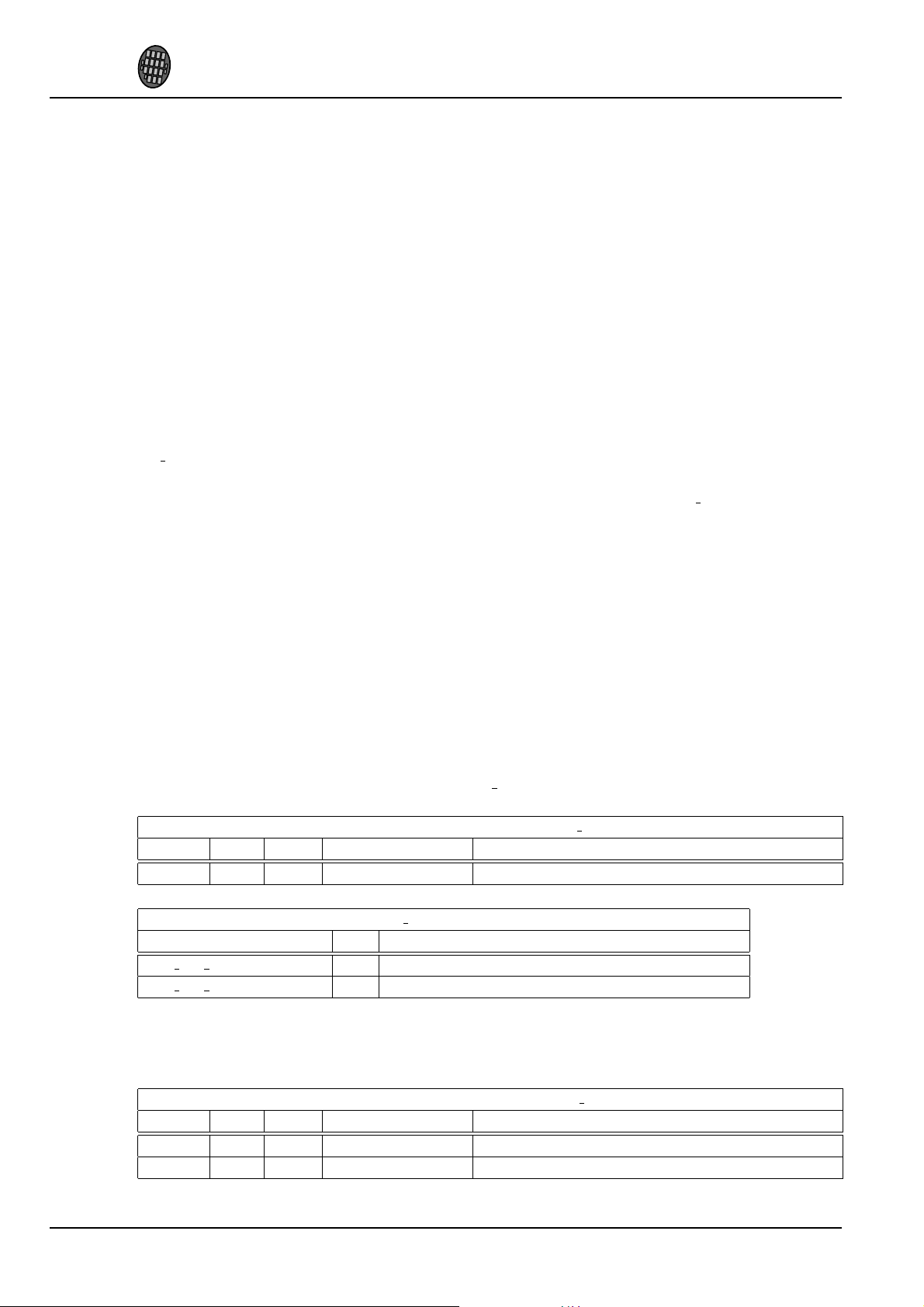
VLSI
Solution
y
VS1033C
VS1033c PRELIMINARY
10. VS1033 REGISTERS
10 VS1033 Registers
10.1 Who Needs to Read This Chapter
User software is required when a user wishes to add some own functionality like DSP effects to VS1033.
However, most users of VS1033 don’t need to worry about writing their own code, or about this chapter,
including those who only download software plug-ins from VLSI Solution’s Web site.
10.2 The Processor Core
VS DSP is a 16/32-bit DSP processor core that also had extensive all-purpose processor features. VLSI
Solution’s free VSKIT Software Package contains all the tools and documentation needed to write, simulate and debug Assembly Language or Extended ANSI C programs for the VS DSP processor core.
VLSI Solution also offers a full Integrated Development Environment VSIDE for full debug capabilities.
10.3 VS1033 Memory Map
VS1033’s Memory Map is shown in Figure 15.
10.4 SCI Registers
SCI registers described in Chapter 8.7 can be found here between 0xC000..0xC00F. In addition to these
registers, there is one in address 0xC010, called SCI CHANGE.
SCI registers, prefix SCI
Reg Type Reset Abbrev[bits] Description
0xC010 r 0 CHANGE[5:0] Last SCI access address
SCI CHANGE bits
Name Bits Description
SCI CH WRITE 4 1 if last access was a write cycle
SCI CH ADDR 3:0 SCI address of last access
10.5 Serial Data Registers
SDI registers, prefix SER
Reg Type Reset Abbrev[bits] Description
0xC011 r 0 DATA Last received 2 bytes, big-endian
0xC012 w 0 DREQ[0] DREQ pin control
Version 0.91, 2007-02-12 57
Page 58

VLSI
Solution
y
VS1033c PRELIMINARY
00000000
Instruction (32−bit) Y (16−bit)X (16−bit)
System Vectors
User
Instruction
RAM
X DATA
RAM
Y DATA
RAM
0030 0030
Y DATA
ROM
X DATA
ROM
4000 4000
Instruction
ROM
C000
C100 C100
C000
0500 0500
8000 8000
Stack Stack
1940
1880
18001800
1880
1940
2800
2000
2800
2000
FFFF FFFF
I/O
User User
VS1033C
10. VS1033 REGISTERS
10.6 DAC Registers
Figure 15: User’s Memory Map.
DAC registers, prefix DAC
Reg Type Reset Abbrev[bits] Description
0xC013 rw 0 FCTLL DAC frequency control, 16 LSbs
0xC014 rw 0 FCTLH DAC frequency control 4MSbs, PLL control
0xC015 rw 0 LEFT DAC left channel PCM value
0xC016 rw 0 RIGHT DAC right channel PCM value
Every fourth clock cycle, an internal 26-bit counter is added to by (DAC FCTLH & 15) × 65536 +
DAC FCTLL. Whenever this counter overflows, valuesfrom DAC LEFT and DAC RIGHT are read and
a DAC interrupt is generated.
Version 0.91, 2007-02-12 58
Page 59

VLSI
Solution
y
VS1033C
VS1033c PRELIMINARY
10. VS1033 REGISTERS
10.7 GPIO Registers
GPIO registers, prefix GPIO
Reg Type Reset Abbrev[bits] Description
0xC017 rw 0 DDR[7:0] Direction
0xC018 r 0 IDATA[7:0] Values read from the pins
0xC019 rw 0 ODATA[7:0] Values set to the pins
GPIO DIR is used to set the direction of the GPIO pins. 1 means output. GPIO ODATA remembers its
values even if a GPIO DIR bit is set to input.
GPIO registers don’t generate interrupts.
Note that in VS1033 the VSDSP registers can be read and written through the SCI WRAMADDR and
SCI WRAM registers. You can thus use the GPIO pins quite conveniently.
Version 0.91, 2007-02-12 59
Page 60

VLSI
Solution
y
VS1033c PRELIMINARY
10. VS1033 REGISTERS
10.8 Interrupt Registers
Interrupt registers, prefix INT
Reg Type Reset Abbrev[bits] Description
0xC01A rw 0 ENABLE[7:0] Interrupt enable
0xC01B w 0 GLOB DIS[-] Write to add to interrupt counter
0xC01C w 0 GLOB ENA[-] Write to subtract from interrupt counter
0xC01D rw 0 COUNTER[4:0] Interrupt counter
INT ENABLE controls the interrupts. The control bits are as follows:
INT ENABLE bits
Name Bits Description
INT EN TIM1 7 Enable Timer 1 interrupt
INT EN TIM0 6 Enable Timer 0 interrupt
INT EN RX 5 Enable UART RX interrupt
INT EN TX 4 Enable UART TX interrupt
INT EN MODU 3 Enable AD modulator interrupt
INT EN SDI 2 Enable Data interrupt
INT EN SCI 1 Enable SCI interrupt
INT EN DAC 0 Enable DAC interrupt
VS1033C
Note: It may take upto 6 clock cycles before changing INT ENABLE has any effect.
Writing any value to INT GLOB DIS adds one to the interrupt counter INT COUNTER and effectively
disables all interrupts. It may take upto 6 clock cycles before writing to this register has any effect.
Writing any value to INT GLOB ENA subtracts one from the interrupt counter (unless INT COUNTER
already was 0). If the interrupt counter becomes zero, interrupts selected with INT ENABLE are restored. An interrupt routine should always write to this register as the last thing it does, because interrupts automatically add one to the interrupt counter, but subtracting it back to its initial value is the
responsibility of the user. It may take upto 6 clock cycles before writing this register has any effect.
By reading INT COUNTER the user may check if the interrupt counter is correct or not. If the register
is not 0, interrupts are disabled.
Version 0.91, 2007-02-12 60
Page 61

VLSI
Solution
y
VS1033C
VS1033c PRELIMINARY
10. VS1033 REGISTERS
10.9 A/D Modulator Registers
Interrupt registers, prefix AD
Reg Type Reset Abbrev[bits] Description
0xC01E rw 0 DIV A/D Modulator divider
0xC01F rw 0 DATA A/D Modulator data
AD DIV bits
Name Bits Description
ADM POWERDOWN 15 1 in powerdown
ADM DIVIDER 14:0 Divider
ADM DIVIDER controls the AD converter’s sampling frequency. To gather one sample, 128 × n clock
cycles are used (n is value of AD DIV). The lowest usable value is 4, which gives a 48 kHz sample rate
when CLKI is 24.576 MHz. When ADM POWERDOWN is 1, the A/D converter is turned off.
AD DATA contains the latest decoded A/D value.
Version 0.91, 2007-02-12 61
Page 62

VLSI
Solution
y
VS1033C
VS1033c PRELIMINARY
10. VS1033 REGISTERS
10.10 Watchdog v1.0 2002-08-26
The watchdog consist of a watchdog counter and some logic. After reset, the watchdog is inactive.
The counter reload value can be set by writing to WDOG CONFIG. The watchdog is activated by writing 0x4ea9 to register WDOG RESET. Every time this is done, the watchdog counter is reset. Every
65536’th clock cycle the counter is decremented by one. If the counter underflows, it will activate vsdsp’s internal reset sequence.
Thus, after the first 0x4ea9 write to WDOG RESET, subsequent writes to the same register with the
same value must be made no less than every 65536×WDOG CONFIG clock cycles.
Once started, the watchdog cannot be turned off. Also, a write to WDOG CONFIG doesn’t change the
counter reload value.
After watchdoghasbeen activated,anyread/write operation from/to WDOG CONFIG or WDOG DUMMY
will invalidate the next write operation to WDOG RESET. This will prevent runaway loops from resetting the counter, even if they do happen to write the correct number. Writing a wrong value to
WDOG RESET will also invalidate the next write to WDOG RESET.
Reads from watchdog registers return undefined values.
10.10.1 Registers
Watchdog, prefix WDOG
Reg Type Reset Abbrev Description
0xC020 w 0 CONFIG Configuration
0xC021 w 0 RESET Clock configuration
0xC022 w 0 DUMMY[-] Dummy register
Version 0.91, 2007-02-12 62
Page 63

VLSI
Solution
y
VS1033C
Start
bit
D0
D1 D2 D3
D4
D5
D6 D7
Stop
bit
VS1033c PRELIMINARY
10. VS1033 REGISTERS
10.11 UART v1.1 2004-10-09
RS232 UART implements a serial interface using rs232 standard.
Figure 16: RS232 Serial Interface Protocol
When the line is idling, it stays in logic high state. When a byte is transmitted, the transmission begins
with a start bit (logic zero) and continues with data bits (LSB first) and ends up with a stop bit (logic
high). 10 bits are sent for each 8-bit byte frame.
10.11.1 Registers
UART registers, prefix UARTx
Reg Type Reset Abbrev Description
0xC028 r 0 STATUS[4:0] Status
0xC029 r/w 0 DATA[7:0] Data
0xC02A r/w 0 DATAH[15:8] Data High
0xC02B r/w 0 DIV Divider
10.11.2 Status UARTx STATUS
A read from the status register returns the transmitter and receiver states.
UARTx STATUS Bits
Name Bits Description
UART ST FRAMEERR 4 Framing error (stop bit was 0)
UART ST RXORUN 3 Receiver overrun
UART ST RXFULL 2 Receiver data register full
UART ST TXFULL 1 Transmitter data register full
UART ST TXRUNNING 0 Transmitter running
UART ST FRAMEERR is set if the stop bit of the received byte was 0.
UART ST RXORUN is set if a received byte overwrites unread data when it is transferred from the
receiver shift register to the data register, otherwise it is cleared.
UART ST RXFULL is set if there is unread data in the data register.
UART ST TXFULL is set if a write to the data register is not allowed (data register full).
UART ST TXRUNNING is set if the transmitter shift register is in operation.
Version 0.91, 2007-02-12 63
Page 64

VLSI
Solution
y
VS1033C
VS1033c PRELIMINARY
10. VS1033 REGISTERS
10.11.3 Data UARTx DATA
A read from UARTx DATA returns the received byte in bits 7:0, bits 15:8 are returned as ’0’. If there is
no more data to be read, the receiver data register full indicator will be cleared.
A receive interrupt will be generated when a byte is moved from the receivershift register to the receiver
data register.
A write to UARTx DATA sets a byte for transmission. The data is taken from bits 7:0, other bits in the
written value are ignored. If the transmitter is idle, the byte is immediately moved to the transmitter shift
register, a transmit interrupt request is generated, and transmission is started. If the transmitter is busy,
the UART ST TXFULL will be set and the byte remains in the transmitter data register until the previous
byte has been sent and transmission can proceed.
10.11.4 Data High UARTx DATAH
The same as UARTx DATA, except that bits 15:8 are used.
10.11.5 Divider UARTx DIV
UARTx DIV Bits
Name Bits Description
UART DIV D1 15:8 Divider 1 (0..255)
UART DIV D2 7:0 Divider 2 (6..255)
The divider is set to 0x0000 in reset. The ROM boot code must initialize it correctly depending on the
master clock frequency to get the correct bit speed. The second divider (D2) must be from 6 to 255.
f
The communication speed f =
m
(D1+1)×(D2)
, where fmis the master clock frequency, and f is the
TX/RX speed in bps.
Divider values for common communication speeds at 26 MHz master clock:
Example UARTSpeeds, f
= 26MHz
m
Comm. Speed [bps] UART DIV D1 UART DIV D2
4800 85 63
9600 42 63
14400 42 42
19200 51 26
28800 42 21
38400 25 26
57600 1 226
115200 0 226
Version 0.91, 2007-02-12 64
Page 65

VLSI
Solution
y
VS1033C
VS1033c PRELIMINARY
10.11.6 Interrupts and Operation
Transmitter operates as follows: After an 8-bit word is written to the transmit data register it will be
transmitted instantly if the transmitter is not busy transmitting the previous byte. When the transmission
begins a TX INTR interrupt will be sent. Status bit [1] informs the transmitter data register empty (or
full state) and bit [0] informs the transmitter (shift register) empty state. A new word must not be written
to transmitter data register if it is not empty (bit [1] = ’0’). The transmitter data register will be empty
as soon as it is shifted to transmitter and the transmission is begun. It is safe to write a new word to
transmitter data register every time a transmit interrupt is generated.
Receiver operates as follows: It samples the RX signal line and if it detects a high to low transition, a
start bit is found. After this it samples each 8 bit at the middle of the bit time (using a constant timer),
and fills the receiver (shift register) LSB first. Finally the data in the receiver is moved to the reveive
data register, the stop bit state is checked (logic high = ok, logic low = framing error) for status bit[4],
the RX INTR interrupt is sent, status bit[2] (receive data register full) is set, and status bit[2] old state is
copied to bit[3] (receive data overrun). After that the receiver returns to idle state to wait for a new start
bit. Status bit[2] is zeroed when the receiver data register is read.
10. VS1033 REGISTERS
RS232 communication speed is set using two clock dividers. The base clock is the processor master
clock. Bits 15-8 in these registers are for first divider and bits 7-0 for second divider. RX sample
frequency is the clock frequency that is input for the second divider.
Version 0.91, 2007-02-12 65
Page 66

VLSI
Solution
y
VS1033C
VS1033c PRELIMINARY
10. VS1033 REGISTERS
10.12 Timers v1.0 2002-04-23
There are two 32-bit timers that can be initialized and enabled independently of each other. If enabled,
a timer initializes to its start value, written by a processor, and starts decrementing every clock cycle.
When the value goes past zero, an interrupt is sent, and the timer initializes to the value in its start value
register, and continues downcounting. A timer stays in that loop as long as it is enabled.
A timer has a 32-bit timer register for down counting and a 32-bit TIMER1 LH register for holding the
timer start value written by the processor. Timers have also a 2-bit TIMER ENA register. Each timer is
enabled (1) or disabled (0) by a corresponding bit of the enable register.
10.12.1 Registers
Timer registers, prefix TIMER
Reg Type Reset Abbrev Description
0xC030 r/w 0 CONFIG[7:0] Timer configuration
0xC031 r/w 0 ENABLE[1:0] Timer enable
0xC034 r/w 0 T0L Timer0 startvalue - LSBs
0xC035 r/w 0 T0H Timer0 startvalue - MSBs
0xC036 r/w 0 T0CNTL Timer0 counter - LSBs
0xC037 r/w 0 T0CNTH Timer0 counter - MSBs
0xC038 r/w 0 T1L Timer1 startvalue - LSBs
0xC039 r/w 0 T1H Timer1 startvalue - MSBs
0xC03A r/w 0 T1CNTL Timer1 counter - LSBs
0xC03B r/w 0 T1CNTH Timer1 counter - MSBs
10.12.2 Configuration TIMER CONFIG
TIMER CONFIG Bits
Name Bits Description
TIMER CF CLKDIV 7:0 Master clock divider
TIMER CF CLKDIV is the master clock divider for all timer clocks. The generated internal clock
f
frequency f
m
=
i
, where fmis the master clock frequency and c is TIMER CF CLKDIV. Example:
c+1
Witha 12 MHz master clock, TIMER CF DIV=3 divides the master clock by 4, and the output/sampling
clock would thus be f
i
=
12MHz
3+1
= 3MHz.
Version 0.91, 2007-02-12 66
Page 67

VLSI
Solution
y
VS1033c PRELIMINARY
10.12.3 Configuration TIMER ENABLE
TIMER ENABLE Bits
Name Bits Description
TIMER EN T1 1 Enable timer 1
TIMER EN T0 0 Enable timer 0
10.12.4 Timer X Startvalue TIMER Tx[L/H]
VS1033C
10. VS1033 REGISTERS
The 32-bit start value TIMER Tx[L/H] sets the initial counter value when the timer is reset. The timer
f
interrupt frequency f
t
=
i
where fiis the master clock obtained with the clock divider (see Chap-
c+1
ter 10.12.2 and c is TIMER Tx[L/H].
Example: Witha 12 MHz master clock andwithTIMER CF CLKDIV=3, the master clock fi= 3MHz.
If TIMER TH=0, TIMER TL=99, then the timer interrupt frequency f
3MHz
=
t
99+1
= 30kHz.
10.12.5 Timer X Counter TIMER TxCNT[L/H]
TIMER TxCNT[L/H] contains the current counter values. By reading this register pair, the user may get
knowledge of how long it will take before the next timer interrupt. Also, by writing to this register, a
one-shot different length timer interrupt delay may be realized.
10.12.6 Interrupts
Each timer has its own interrupt, which is asserted when the timer counter underflows.
Version 0.91, 2007-02-12 67
Page 68
VLSI
Solution
y
VS1033c PRELIMINARY
MCLK
SDATA
SCLK
LROUT
MSB LSB MSB
Left Channel Word Right Channel Word
10.13 I2S DAC Interface
The I2S Interface makes it possible to attach an external DAC to the system.
10.13.1 Registers
I2S registers, prefix I2S
Reg Type Reset Abbrev Description
0xC040 r/w 0 CONFIG[3:0] I2S configuration
10.13.2 Configuration I2S CONFIG
I2S CONFIG Bits
Name Bits Description
I2S CF MCLK ENA 3 Enables the MCLK output (12.288 MHz)
I2S CF ENA 2 Enables I2S, otherwise pins are GPIO
I2S CF SRATE 1:0 I2S rate, ”10” = 192, ”01” = 96, ”00” = 48 kHz
VS1033C
10. VS1033 REGISTERS
I2S CF ENA enables the I2S interface. After reset the interface is disabled and the pins are used for
GPIO.
I2S CF MCLK ENA enables the MCLK output. The frequency is either directly the input clock (nominal 12.288 MHz), or half the input clock when mode register bit SM CLK RANGE is set to 1 (2426 MHz input clock).
I2S CF SRATE controls the output samplerate. When set to 48 kHz, SCLK is MCLK divided by 8,
when 96 kHz SCLK is MCLK divided by 4, and when 192 kHz SCLK is MCLK divided by 2.
Figure 17: I2S Interface, 192 kHz.
To enable I2S first write 0xc017 to SCI WRAMADDR and 0x33 to SCI WRAM, then write 0xc040 to
SCI WRAMADDR and 0x0c to SCI WRAM.
See application notes for more information.
Version 0.91, 2007-02-12 68
Page 69

VLSI
Solution
y
VS1033C
VS1033c PRELIMINARY
10. VS1033 REGISTERS
10.14 System Vector Tags
The System Vector Tags are tags that may be replaced by the user to take control over several decoder
functions.
10.14.1 AudioInt, 0x20
Normally contains the following VS DSP assembly code:
jmpi DAC_INT_ADDRESS,(i6)+1
The user may, at will, replace the first instruction with a jmpi command to gain control over the audio
interrupt.
10.14.2 SciInt, 0x21
Normally contains the following VS DSP assembly code:
jmpi SCI_INT_ADDRESS,(i6)+1
The user may, at will, replacetheinstructionwitha jmpi command to gaincontrolover the SCIinterrupt.
10.14.3 DataInt, 0x22
Normally contains the following VS DSP assembly code:
jmpi SDI_INT_ADDRESS,(i6)+1
The user may, atwill,replacetheinstruction with a jmpi commandtogain control over theSDIinterrupt.
10.14.4 ModuInt, 0x23
Normally contains the following VS DSP assembly code:
Version 0.91, 2007-02-12 69
jmpi MODU_INT_ADDRESS,(i6)+1
The user may, at will, replace the instruction with a jmpi command to gain control over the AD Modulator interrupt.
Page 70

VLSI
Solution
y
VS1033C
VS1033c PRELIMINARY
10.14.5 TxInt, 0x24
Normally contains the following VS DSP assembly code:
jmpi EMPTY_INT_ADDRESS,(i6)+1
The user may, at will, replace the instruction with a jmpi command to gain control over the UART TX
interrupt.
10.14.6 RxInt, 0x25
Normally contains the following VS DSP assembly code:
jmpi RX_INT_ADDRESS,(i6)+1
10. VS1033 REGISTERS
The user may, at will, replace the first instruction with a jmpi command to gain control over the UART
RX interrupt.
10.14.7 Timer0Int, 0x26
Normally contains the following VS DSP assembly code:
jmpi EMPTY_INT_ADDRESS,(i6)+1
The user may, at will, replace the first instruction with a jmpi command to gain control over the Timer
0 interrupt.
10.14.8 Timer1Int, 0x27
Normally contains the following VS DSP assembly code:
jmpi EMPTY_INT_ADDRESS,(i6)+1
The user may, at will, replace the first instruction with a jmpi command to gain control over the Timer
1 interrupt.
Version 0.91, 2007-02-12 70
Page 71

VLSI
Solution
y
VS1033C
VS1033c PRELIMINARY
10.14.9 UserCodec, 0x0
Normally contains the following VS DSP assembly code:
jr
nop
If the user wants to take control away from the standard decoder, the first instruction should be replaced
with an appropriate j command to user’s own code.
Unless the user is feeding MP3 or WMA data at the same time, the system activates the user program
in less than 1 ms. After this, the user should steal interrupt vectors from the system, and insert user
programs.
10. VS1033 REGISTERS
10.15 System Vector Functions
The System Vector Functions are pointers to some functions that the user may call to help implementing
his own applications.
10.15.1 WriteIRam(), 0x2
VS DSP C prototype:
void WriteIRam(register i0 u int16 *addr, register a1 u int16 msW, register a0 u int16 lsW);
This is the preferred way to write to the User Instruction RAM.
10.15.2 ReadIRam(), 0x4
VS DSP C prototype:
u int32 ReadIRam(register i0 u int16 *addr);
This is the preferred way to read from the User Instruction RAM.
A1 contains the MSBs and A0 the LSBs of the result.
10.15.3 DataBytes(), 0x6
VS DSP C prototype:
Version 0.91, 2007-02-12 71
Page 72

VLSI
Solution
y
VS1033C
VS1033c PRELIMINARY
u int16 DataBytes(void);
If the user has taken over the normal operation of the system by switching the pointer in UserCodec
to point to his own code, he may read data from the Data Interface through this and the following two
functions.
This function returns the number of data bytes that can be read.
10.15.4 GetDataByte(), 0x8
VS DSP C prototype:
u int16 GetDataByte(void);
Reads and returns one data byte from the Data Interface. This function will wait until there is enough
data in the input buffer. Audio interrupts must be enabled for this function to work.
10. VS1033 REGISTERS
10.15.5 GetDataWords(), 0xa
VS DSP C prototype:
void GetDataWords(register i0 y u int16 *d, register a0 u int16 n);
Read n data byte pairs and copy them in big-endian format (first byte to MSBs) to d. This function will
wait until there is enough data in the input buffer. Audio interrupts must be enabled for this function to
work.
Version 0.91, 2007-02-12 72
Page 73

VLSI
Solution
y
VS1033C
VS1033c PRELIMINARY
11. DOCUMENT VERSION CHANGES
11 Document Version Changes
This chapter describes the most important changes to this document.
11.1 Version 0.91 for VS1033c, 2007-02-12
• GBUF connection in Connection diagram changed (figure 3 in section 6).
GBUF must have 10Ω and 47 nF to ground.
• Mention of the 8 kHz Phone Application removed. Other features have replaced this code in
VS1033c.
11.2 Version 0.9 for VS1033c, 2006-08-15
• EarSpeaker documentation added.
11.3 Version 0.8 for VS1033b, 2006-05-19
• Mention of quiet power-off added to feature list.
11.4 Version 0.6 for VS1033a, 2006-01-05
• ADPCM recording section added (section 9.4)
11.5 Version 0.5, 2005-10-21
• More detailed info about fast forward / rewind.
Version 0.91, 2007-02-12 73
Page 74

VLSI
Solution
y
VS1033c PRELIMINARY
12 Contact Information
VLSI Solution Oy
Entrance G, 2nd floor
Hermiankatu 8
FIN-33720 Tampere
FINLAND
Fax: +358-3-3140-8288
Phone: +358-3-3140-8200
Email: sales@vlsi.fi
URL: http://www.vlsi.fi/
VS1033C
12. CONTACT INFORMATION
Version 0.91, 2007-02-12 74
 Loading...