

Page 1
Service Manual
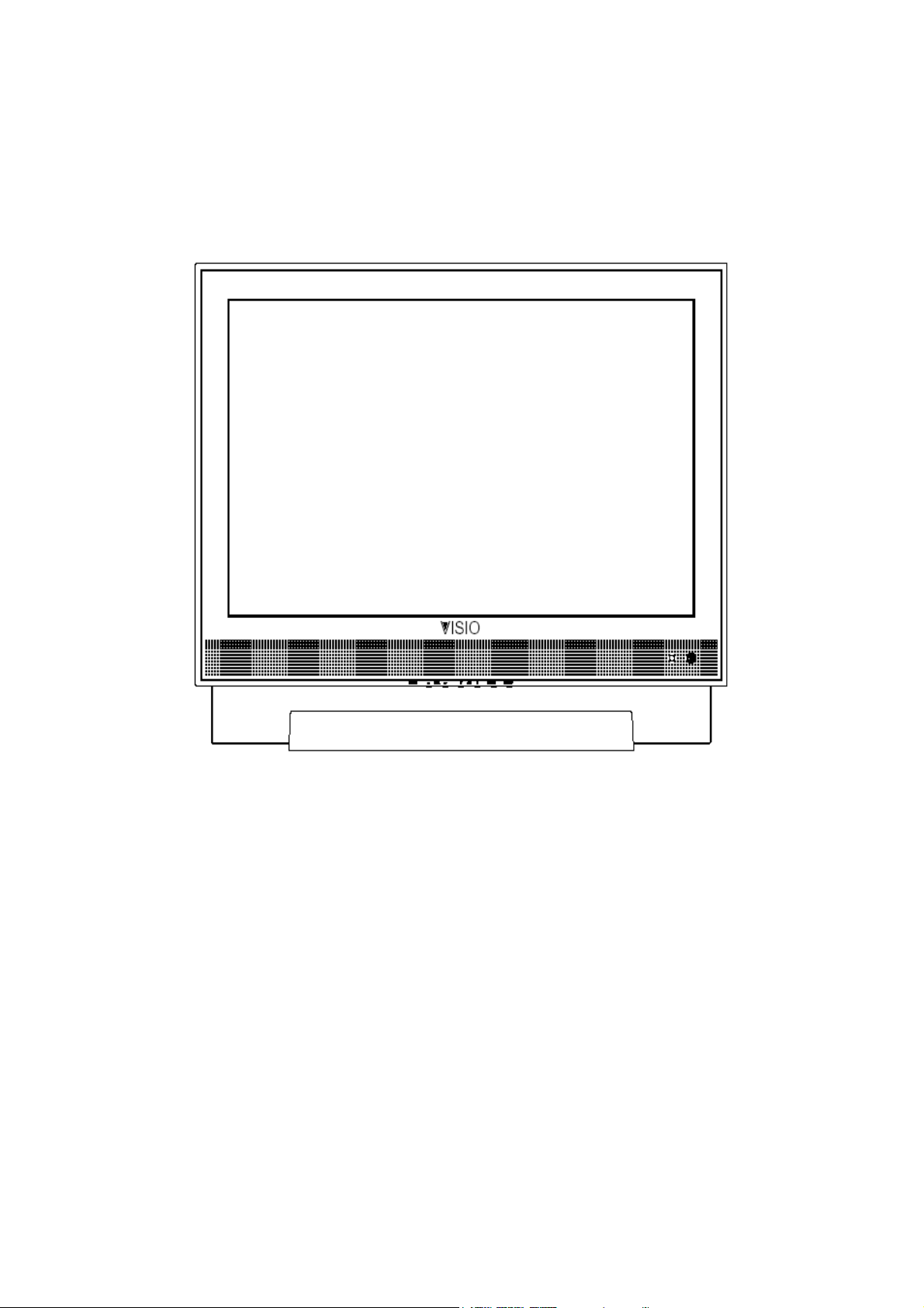
Model #: VIZIO L30WGU
V, Inc
320A Kalmus Drive Costa Mesa, CA 92626
TEL : +714-668-0588 FAX :+714-668-9099
Top Confidential
Page 2

Table of Contents
CONTENTS PAGE
Sections
1. Features 1-1
2. Specifications 2-1
3. On Screen Display 3-1
4. Factory Preset Timings
5. Pin Assignment
4-1
5-1
6. BLOCK DIAGRAM 6-1
7. Main Board I/O Connections 7-1
8. Theory of Circuit Operation 8-1
9. Waveforms 9-1
10. Trouble Shooting 10-1
11. Spare Parts List 11-1
12. Complete Parts List 12-1
Appendix
1. Main Board Circuit Diagram
2. Main Board PCB Layout
3. Assembly Explosion Drawing
Block Diagram
VIZIO L30WGU Service Manual
Page 3

VINC Service Manual
VIZIO L30WGU
COPYRIGHT © 2000 V, INC. ALL RIGHTS RESERVED.
IBM and IBM products are registered trademarks of International Business Machines
Corporation.
Macintosh and Power Macintosh are registered trademarks of Apple Computer, Inc.
VINC and VINC products are registered trademarks of V, Inc.
VESA, EDID, DPMS and DDC are registered trademarks of Video Electronics Standards
Association (VESA).
Energy Star is a registered trademark of the US Environmental Protection Agency (EPA).
No part of this document may be copied, reproduced or transmitted by any means for any
purpose without prior written permission from VINC.
FCC INFORMATION
This equipment has been tested and found to comply with the limits of a Class B digital device,
pursuant to part 15 of the FCC Rules. These limits are designed to provide reasonable
protection against harmful interference in a residential installation. This equipment generates,
uses and can radiate radio frequency energy, and if not installed and used in accordance with
the instructions, may cause harmful interference to radio communications. However, there is
no guarantee that the interference will not occur in a particular installation. If this equipment
does cause unacceptable interference to radio or television reception, which can be
determined by turning the equipment off and on, the user is encouraged to try to correct the
interference by one or more of the following measures -- reorient or relocate the receiving
antenna; increase the separation between equipment and receiver; or connect the into an
outlet on a circuit different from that to which the receiver is connected.
FCC WARNING
To assure continued FCC compliance, the user must use a grounded power supply cord and
the provided shielded video interface cable with bonded ferrite cores. Also, any unauthorized
changes or modifications to Amtrak products will void the user’s authority to operate this
device. Thus VINC Will not be held responsible for the product and its safety.
CE CERTIFICATION
This device complies with the requirements of the EEC directive 89/336/EEC with regard to
“Electromagnetic compatibility.”
SAFETY CAUTION
Use a power cable that is properly grounded. Always use the AC cords as follows – USA (UL);
Canada (CSA); Germany (VDE); Switzerland (SEV); Britain (BASEC/BS); Japan (Electric
Appliance Control Act); or an AC cord that meets the local safety standards.
VIZIO L30WGU Service Manual
Page 4

Chapter 1 Features
1. Built in TV channel selector for TV viewing
2. Simulatnueous display of PC and TV images
3. Connectable to PC’s analog RGB port and digital port
4. Connectable to digital port HDCP
4. Built in s-video, HDTV, composite video and TV out
5. Built in auto adjust function for automatic adjument of screen display
6. Smoothing function enables display of smooth texts and graphics even if image
withresolution lower than 1280x768 is magnified
7. Picture In Picture (PIP) funtion to show TV or VCR images
8. Power saving to reduce consumption power too less than 3W
9. On Screen Display: user can define display mode (ie color, brightness, contrast,
sharpness), sound setting, PIP, TV channel program, aspect and gamma or
reset to factory setting.
CONFIDENTIAL – DO NOT COPY
Page 1-1
File No. SG-0156
Page 5

Chapter 2 Specification
1. LCD CHARACTERISTICS
Type: WXGA TFT LCD
Size: 30 inch
Active Screen Size: 29.53 inches
Outline Dimension: 683.6(H) x 431.8(V) x 41.6(D)
Display Area: 643.20 (H) x 385.92(V)
Pixel Format: 1280 horiz. By 768 vert. Pixels RGB strip arrangement
Display Color: 16.7M colors
Luminance, White: 600 cd/m
2 (Typ)
Power Consumption: 6.6Watt (Typ.)
Weight 5000 g (Typ.)
Display Operating Mode: Transmissive mode, normally Black
Surface Treatment: Hard coating (2H), Anti-glare treatment of the front polarizer,
2. OPTICAL CHARACTERISTICS
2-1. Viewing Angle by Contrast Ratio °Ÿ 10
Left: 85°typ.
Right: 85°typ.
Top: 85°typ.
Bottom: 85°typ.
3. SIGNAL (Refer to the Timing Chart)
3-1. Sync Signal
(1) Type: TMDS
(2) Input Voltage Level: 90~240 Vac, 50/ 60 Hz
(3) Input Impedance: 50£[/ Signal line
3-2. Operating Frequency
RGB Signal: H: support to 30K~70KHz
V: support to 50~85Hz
Pixel Clock: support to 110MHz
DVI Signal: H: support to 30K~80KHz
V: support to 50~85Hz
Pixel Clock: support to 110MHz
CONFIDENTIAL – DO NOT COPY
Page 2-1
File No. SG-0156
Page 6

S-Video Video (Y): Analog 0.1Vp-p/75Ω
Video (C): Analog 0.286p-p/75Ω
Component signal: YCbCr
H: 15.734KHz V: 60Hz (NTSC-interlace)
H: 31KHz V: 60Hz (NTSC-progressive)
YPbPr
H: 15.734KHz V: 60Hz (NTSC-480i)
H: 31KHz V: 60Hz(NTSC-480p)
H: 45KHz V: 60Hz(NTSC-720p)
H: 33KHz V: 60Hz(NTSC-1080i)
Composite Video signal: H: 15.734KHz V: 60Hz (NTSC)
F-Type TV RF signal: H: 15.734KHz V: 60Hz (NTSC)
Audio Signal: Frequency Response: 250 Hz-20KHz
4.Input Connectors
a. RJ11 (For RS232 Controls)
b. 24-pin DVI (For DVI/HDCP input)
c. RCA x2 ((For DVI/HDCP input)
d. D-sub 15pin x 1 (For Analog RGB)
e.Mini Jack (L,R) x 1 (For PC analog Audio input)
f. YPbPr RCA x 3 (For HDTV input)
g. YCbCr RCA x 3 (For DVD input)
h. S-Video 4pin DIN x 1
i. RCA x3 (For CVBS A/V input#1)
j. RCA x 3(For CVBS A/V input#2)
k. F-terminal RF
l. CVBS RCA x 3 (For CVBS A/V output)
5. POWER SUPPLY
Consumption: 170W MAX
DPM Mode Not Active OFF: less than 3 W Low (20%)
Power OFF: to less than 3W
CONFIDENTIAL – DO NOT COPY
Page 2-2
File No. SG-0156
Page 7

6.Speaker
Output 8Ω/5W (max) X2
7. ENVIRONMENT
Operating
a. Temperature: 5~35℃
b. Relative humidity: 10~90%
c. Altitude: 0~10,000ft
Non-operating
a. Temperature: -20~50℃
b. Relative humidity: 10~90%
c. Altitude: 0~40,0000ft
8. DIMENSIONS (with TILT/SWIVEL)
GATEWAY VERSION
a. Height: 601.1mm
b. Width: 740.0mm
c. Depth: 198.0mm
Wynn version
a. Height: 522.0mm
b. Width: 740.0mm
c. Depth: 100.5mm
9. WEIGHT (with TILT/SWIVEL)
GATEWAY version
a. Net: 19.1kgs
b. Gross: 25.8kgs
Wynn version
a. Net: 14.1kgs
b. Gross: 20.8kgs
CONFIDENTIAL – DO NOT COPY
Page 2-3
File No. SG-0156
Page 8

Chapter 3 On Screen Display
Main unit button
Power
Source
MENU
PROG ▲
PROG ▼
Sound +
Sound -
Auto
OSD Adjustment
1. PC Analog
A. Picture:
a. Brightness
b. Contrast
c. Auto picture
d. Manual picture:
e. Sharpness: 1~5
f. Color Temp (User, 9300k, 6500k, 5000k)
B. Audio:
a. Volume
1. V position
2. H size
3. H position
4. Fine tune
1. R (Red setting) (0~100)
2. G (Green setting) (0~100)
3. B (Blue setting) (0~100)
b. Treble
c. Bass
d. Balance
e. Spatial
CONFIDENTIAL – DO NOT COPY
Page 3-1
File No. SG-0156
Page 9

C. Setup:
a. Language (English, France, Spain)
b. Gamma (Linear, Vivid1, Vivid2, Vivid3)
c. Wide (Panoramic, Widescreen, Zoom, Standard)
d. PiP:
1. Switch (On/Off)
2. Style (Off, Small, Large)
3. Pos (Upper left, Upper center, Upper right
Middle left, Middle right, lower left, lower center, lower left)
4. Source (TV, DVD, AV2/S, AV1)
5. PiP TV Channel
e. OSD style (Translucent, Opaque)
f. IR Command Set (A, B, C)
2. PC digital
A. Picture:
a. Brightness
b. Contrast
c. Sharpness
d. Color Temp
B. Audio:
a. Volume
b. Treble
c. Bass
d. Balance
e. Spatial
C. Setup:
User, 5000k, 6500k, 9300k
R (Red setting)
G (Green setting)
B (Blue setting)
a. Language (English, France, Spain)
b. Gamma (Linear, Vivid1, Vivid2, Vivid3)
c. Wide (Panoramic, Widescreen, Zoom, Standard)
d. PiP:
CONFIDENTIAL – DO NOT COPY
Page 3-2
File No. SG-0156
Page 10

1. Switch (On/Off)
2. Style (Off, Small, Large)
3. Pos (Upper left, Upper center, Upper right
Middle left, Middle right, lower left, lower center, lower left)
4. Source (TV, DVD, AV2/S, AV1,)
5. PiP TV Channel
e. OSD style (Translucent, Opaque)
f . IR Command Set (A, B, C)
3.AV2/S, AV1, DVD, HDTV Mode
A. Video:
a. Brightness
b. Contrast
c. Color
d. Tint
e. Sharpness (1~5)
f. Color Temp (normal, Warm, Cool)
g. Noise Reduct
B. Audio:
a. Volume
b. Treble
c. Bass
d. Balance
e. Spatial
C. Setup:
a. Language (English, France, Spain)
b. Gamma (Linear, Vivid1, Vivid2, Vivid3)
c. Wide (Panoramic, Widescreen, Zoom, Standard)
d. PiP:
1. Switch (On/Off)
2. Style (Off, Small, Large)
3. Pos (Upper left, Upper center, Upper right
Middle left, Middle right, lower left, lower center, lower left)
4. Source (TV, DVD, AV2/S, AV1)
5. PiP TV Channel
e. OSD style (Translucent, Opaque)
f . IR Command Set (A, B, C)
CONFIDENTIAL – DO NOT COPY
Page 3-3
File No. SG-0156
Page 11

4. TV
A. Video:
a. Brightness
b. Contrast
c. Color
d. Tint
e. Sharpness
f. Color Temp (normal, Warm, Cool)
g. Noise Reduct
B. Audio:
a. Volume
b. Treble
c. Bass
d. Balance
e. Spatial
f. MTS (Mono, Stereo, SAP)
C. TV:
a. Source (Antenna, Cable)
b. Cable mode (auto, std, Hrc, irc)
c. Channel scan
d. CC Mode (CC1, CC2 Text1, Text2)
e. Parental Control
1. Change password (New password, Confirm password)
2. Setup TV Blocking
3. Setup Movie Blocking
4. Blocking Enable (On/Off)
5. Key Lockout (On, Off, All, All but power)
6. IR Lockout (On/Off)
7. Factory reset (Yes/No)
D. Setup:
a. Language (English, France, Spain)
b. Gamma (Vivid1, Vivid2, Vivid3 and liner)
c. Wide (Panoramic, Widescreen, Zoom and Standard)
d. PiP
1. Switch (On/Off)
2. Style (Off, Small, Large)
3. Pos (Upper left, Upper center, Upper right
CONFIDENTIAL – DO NOT COPY
Page 3-4
File No. SG-0156
Page 12

Middle left, Middle right, lower left, lower center, lower left)
4. Source (TV, DVD, AV2/S, AV1)
5. PiP TV Channel
e. OSD style (Translucent, Opaque)
f . IR Command Set (A, B, C)
CONFIDENTIAL – DO NOT COPY
Page 3-5
File No. SG-0156
Page 13
Chapter 4 Factory preset timings
This timing chart is already preset for the TFT LCD analog & digital display monitors.
Resolution Refresh rate
Horizontal
Frequency
640x480 60Hz 31.5kHz 59.94Hz N N 25.175
640x480 75Hz 37.5kHz 75.00Hz N N 31.500
800X600 60Hz 37.9kHz 60.317Hz P P 40.000
800x600 75Hz 46.9kHz 75.00Hz P P 49.500
800X600 85Hz 53.7kHz 85.06Hz P P 56.250
1024x768 60Hz 48.4kHz 60.01Hz N N 65.000
1024X768 75Hz 60.0kHz 75.03Hz P P 78.750
720x400 70Hz 31.46kHz 70.08Hz N P 28.320
1280x768 60Hz 47.98kHz 59.83Hz P N 81.000
1280x768 75Hz 60.15kHz 75.00Hz P N 102.977
Remark: P: positive N: negative
Vertical
Frequency
Horizontal
Polarity
Vertical
Polarity
Pixel
Rate
Native Resolution
Mode No Resolution
Refresh
Rate
(Hz) (K Hz) (Hz) (TTL) (TTL) (MHz)
9 1280x768 60 47.98 59.83 - + 81MHz
10 1280x768 75 60.15 75.00 - + 102.977MHz
Horizontal
Frequency
Vertical
Frequency
Vertical
Sync
Polarity
Horizontal
Sync
Polarity
Dot rate
CONFIDENTIAL – DO NOT COPY
File No. SG-0156
Page 4-1
Page 14
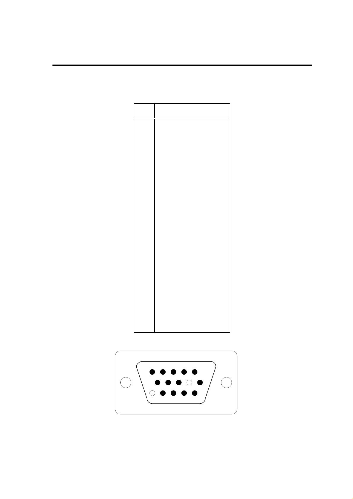
Chapter 5 Pin Assignment
The TFT LCD analog display monitors use a 15 Pin Mini D-Sub connector as
video input source.
Pin Description
1 Red
2 Green
3 Blue
4 Ground
5 Ground
6 R-Ground
7 G-Ground
8 B-Ground
9 +5V for DDC
10 Ground
11 No Connection
12 (SDA)
13 H-Sync (Composite Sync)
14 V-Sync
15 (SCL)
1
5
106
CONFIDENTIAL – DO NOT COPY
11
15
Page 5-1
File No. SG-0156
Page 15

The TFT LCD digital display monitors use a 24 Pin DVI_D connector as video
input source.
Pin Description
1 TMDS negative differential input, channel 2
2 TMDS positive differential input, channel 2
3 Logic Ground
4 Reserved. No connection
5 Reserved. No connection
6 DDC2B Clock
7 DDC2B Data
8 Reserved. No connection
9 TMDS negative differential input, channel 1
10 TMDS positive differential input, channel 1
11 Logic Ground
12 Reserved. No connection
13 Reserved. No connection
14 Power
15 Logic Ground
16 SENSE Pin, Pull High
17 TMDS negative differential input, channel 0
18 TMDS positive differential input, channel 0
19 Logic Ground
20 Reserved. No connection
21 Reserved. No connection
22 Logic Ground
23 TMDS positive differential input, reference clock
24 TMDS negative differential input, reference clock
CONFIDENTIAL – DO NOT COPY
Page 5-2
File No. SG-0145
Page 16

Four-Pin mini DIN S-Video Connector
Signal Level Video (Y) : Analog 0.1Vp-p/75Ω
Video (C) : Analog 0.286p-p/75
Sync (H+V) : 0.3V below Video (Y)
Frequency H: 15.734Khz V: 60HZ (NTSC)
Video Output Connector
Signal Level Video (Y+C) : Analog 0.7Vp-p/75Ω
Sync (H+V): 0.3V below Video (Y+C)
RGB Signal
a. Sync Type TTL (Separate / Composite) or Sync. On Green
b. Sync polarity Positive or Negative
c. Video Amplitude RGB: 0.7 Vp-p
d. Frequency H: support to 30k~70kHZ
V: support to 50~85MHZ
Audio Signal:
a. Signal Level 1Vrms
b. Frequency Response 250HZ – 20kHZ
CONFIDENTIAL – DO NOT COPY
Page 5-3
File No. SG-0145
Page 17

Component Signal
Ycbcr
a. Frequency H: 15.734kHZ V: 60HZ (NTSC-interlace)
H: 31kHZ V: 60HZ (NTSC-progressive)
b. Signal level Y: 1Vp-p Cb: ±0.350Vp-p Cr: ±0.350Vp-p
c. Impedance 75Ω
Ypbpr
a. Frequency H: 15.764kHZ V: 60HZ (NTSC-480i)
H: 31kHZ V: 60HZ (NTSC-480p)
H: 45kHZ V: 60HZ(NTSC-720p)
H: 33kHZ V: 60HZ(NTSC-1080i)
b. Signal level Y: 1Vp-p pb±0.350Vp-p pr: ±0.350Vp-p
c. Impedance 75Ω
CONFIDENTIAL – DO NOT COPY
Page 5-4
File No. SG-0145
Page 18
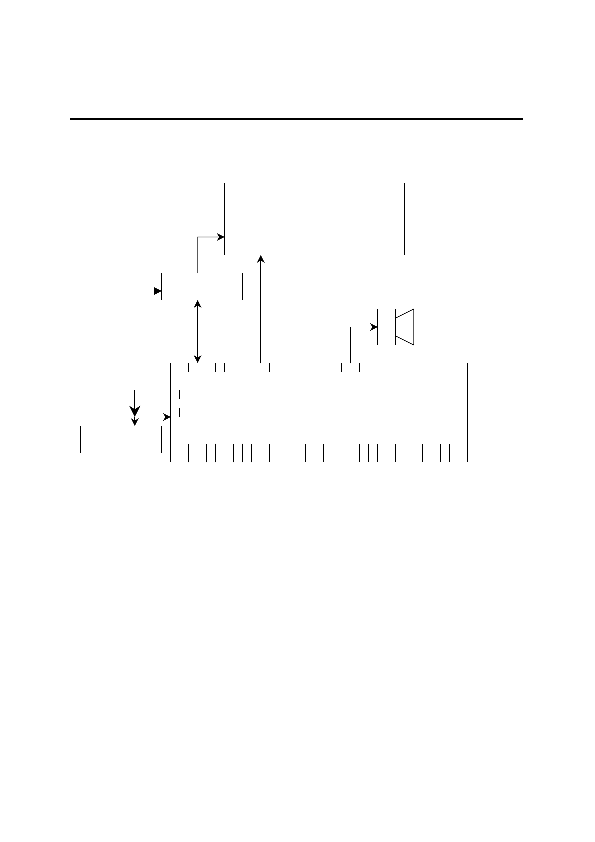
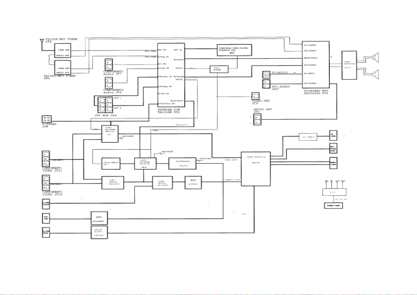
Chapter 6 Block Diagram
System Block Diagram
30” WXGA panel
Digital
AC IN Video bus
Power Board
DC 12V Speakers
□□□□□
W6 W5 JT2
W3 Main Board
W4
W9 W1 JT3 JT11 JT10 JT8 JT5
Keypad/IR
Board DVI D-Sub Audio YPbPr YCbCr S-Video AV1/AV2 RF
The monitor’s system block diagram is powered by power board that transforms AC source of
100V~240V AC +/- 10% @ 50/60 HZ into DC 12V & 24Vsource. The DC source supplies three
important parts of the system block diagram. They are the main board, and 30” WXGA panel unit.
The main board receives different types of video signal. Afterward, the main board process the signals
control the various functions of the monitor and outputs control signal, video signal and power to the
30” WXGA panel to be displayed.
The inverter first processes the power send to the panel. The function of the inverter is to step up the
voltage supplied by the main board to the power that is needed to light up the lamps in the panel.
Simultaneously, the digital video signals are processed in the panel and the outcome determines the
brightness, pixel on/off and the color displayed on the panel.
CONFIDENTIAL – DO NOT COPY
File No. SG-0156
Page 6-1
Page 19
CONFIDENTIAL – DO NOT COPY
Page 6-2
File No. SG-0145
Page 20

The function of the Main board is to receive different types of video and audio signal in to
compatible digital video and audio format.
The FQ1236-MK3 tuner processes the TV antenna and the cable into analog signal.
The audio signal exiting from FQ1236-MK3 is further processed by MSP3440G. The purpose
is to process the input IF signal into AF signal and control TV sound signal features like
volume, bass, treble and balance. The processing procedure conforms to standard
recommend for Broadcast Television System Committee (BTSC).
The analog video signals of S-video, YPbPr, TV and A/V signals travel directly to video
decoder. At the decoder, all signals are translated from analog signals into compatible digital
signal which will be ultimately be processed by theVP3230 & SAA7118.
After the video signal has been converted into digital signals, the digital video signal is
de-interlaced by FLI3210. The de-interlace processor automatically determines and
de-interlace the incoming video content – static or motion and applies different algorithm to
each of the content type. An external SDRAM is used to help store the video fields and
motion video data processed in FLI3210. More over, the internal memory controller in
FLI3210 controls the external SDRAM. What’s more, FLI3210 offer programmable functions
like video enhancement and PIP (picture in picture). PIP functions by activating the primary
and secondary port simultaneously. In short, FLI3210 output (display port) digital signals up
to 74 Mpixel/sec to the PW166B generate the vertical and horizontal timing signals for
display device.
All functions are controllable by the main board. Plus, all functions in the IC boards are
programmable using I2C Bus.
CONFIDENTIAL – DO NOT COPY
Page 6-3
File No. SG-0145
Page 21
Chapter 7 Main Board I/o Connections
W3 CONNECTION (TOP→BOTTOM) "OSD CONTROL
Pin Description
1 “Auto”
2 “Left”
3 “Right”
4 “Down”
5 “Gnd”
6 “Up”
7 “Menu”
8 “Source”
W4 CONNECTION (TOP→BOTTOM)
Pin Description
1 “Power”
2 “U17”
3 “V50”
4 “Gnd”
5 “Vpcon”
W6 CONNECTION (TOP→BOTTOM)
Pin Description
1 “V120dc”
2 “V120dc”
3 “V120dc”
4 “Gnd”
5 “Gnd”
6 “Gnd”
7 “Bk_Light”
8 “Pwm_p”
CONFIDENTIAL – DO NOT COPY
Page 7-1
File No. SG-0156
Page 22

Chapter 8 Theory of Circuit Operation
The operation of D-SUB 15pin route
The D-SUB 15pin is input analog signal into the video switch M61323fp. Then, the signal is process
to the A/D converter (ADC9883) and output to the pw166B; the pw166B generates the vertical and
horizontal timing signals for display device.
The operation of DVI & HDCP CON route
The DVI & HDCP CON is input digital signal the signal is process to the sil169. Then transfer to the
pw166B, the pw166B generates the vertical and horizontal timing signals for display device.
The operation of HDTV & DVD route
HDTV & DVD signal is transfer to video switch M61323fp, the M61323fp can to determine signal
witch one signal is to the VP3230 (decoder) and witch one is to ADC9883. When signal transfer for
the VP3230 (decoder) and output to FLI2310 (de-interlace) then transfer the pw166B generates the
vertical and horizontal timing signals for display device. When signal to the ADC9883 then output to
pw166B generates the vertical and horizontal timing signals for display device. The pip mode is
signal to saa7118 (decoder) then transfer to the pw166B generates the vertical and horizontal timing
signals for display device.
The operation of S-Video route
The S-Video signal is input to TA1218N (switch) then transfer signal to VP3230 (decoder) and output
to FLI2310 (de-interlace) then use graphic port transfer signal to pw166B generates the vertical and
horizontal timing signals for display device. The pip mode is signal to saa7118 (decoder) then
transfer to the pw166B generates the vertical and horizontal timing signals for display device.
The operation of Video 1,2 route
Video 1,2 signal input to TA1218N (switch) and transfer signal to VP3230 (decoder) and output to
FLI2310 (de-interlace), then transfer to the pw166B generates the vertical and horizontal timing
signals for display device. The pip mode is transfer to saa7118 (decoder) then transfer to the
pw166B generates the vertical and horizontal timing signals for display device.
The operation of TV route
TV signal is processes to the tuner and output to TA1218N (switch) then transfer to VP3230
(decoder) and output toFLI2310 (de-interlace) then transfer to pw166B generates the vertical and
horizontal timing signals for display device. The pip mode is signal to saa7118 (decoder) then
transfer to the pw166B generates the vertical and horizontal timing signals for display device.
CONFIDENTIAL – DO NOT COPY
File No. SG-0156
Page 8-1
Page 23
The operation of keypad
There are 8 keys to control and select the function of SHD-3010 and also have two LED to indicate
the status of operation. They are “power, Source, MENU, ▼▲, + -, Auto” keys and LED.
1. The power key through POW and GND to control PW166B, PW166B will receive a low signal to
turn on or off system while press the power key.
2. The other seven keys are on high state because the pull up resistor but will transit to low state
dependent on which key pressed, and the state will be reader by PW166B through D0 to D6 to act
corresponding function.
3. The LED is constructed with two separate LED which color is blue and Green. The PW166B direct
control the LED’s when PW166B (VPCON) is low the LED is Green (Close power) when PW166B
(VPCON) is high the LED is Orange (Open power).
The operation of Analog port
The analog port are consisted with 15 pins mini D-Sub connector which receiving video signal from
host device, EEPROM which compliance with DDC1/DDC2B protocol, H-sync and V-sync detecting
circuit which regenerate synchronous signal for PW166B detecting, video signal matching circuit and
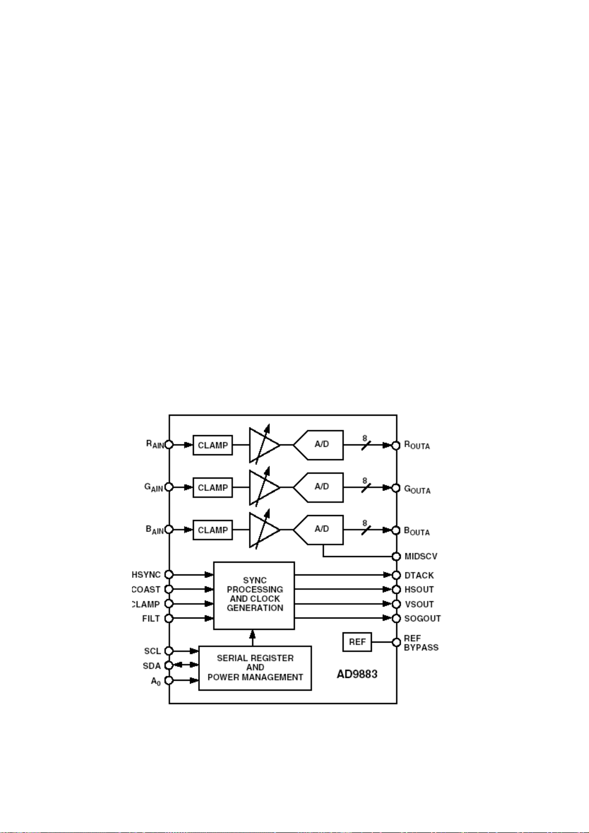
AD9883A which capturing RGB graphics signal and digitize each pixel.
The pin assignment of 15 pins connector are as follows:
Pin No. Pin Name Description
1 GRAI Red signal
2 GGAI Green signal
3 GBAI Blue signal
4 GND Ground
5 GND Ground
6 GND R-Ground
7 GND G-Ground
8 GND B-Ground
9 +5V For DDC
10 GND Ground
11 X No connection
12 RGSA SDA
13 GHSI H-Sync
14 RVSI V-Sync
15 RGSL SCL
CONFIDENTIAL – DO NOT COPY
Page 8-2
File No. SG-0156
Page 24
RGB graphics signal of host device transmits to the analog port through pin 1 to 3. The video signal
should be coupled to RIN, GIN, BIN and SOGIN of AD9883A through C78, C75, C74 and C76. The
EDID data is stored in EEPROM (24LC21) which compliance with DDC1/DDC2B protocol that
performs a plug and play function. When in DDC1 protocol the host device access the EDID data
through RVSI (pin14) and RGSA (pin12) while RGSL (pin15) is held high. But in DDC2B protocol the
host device access EDID data through RGSA (pin12) and RGSL (pin15). The SCL, SDA should be
pull up through R28 R27 and are voltage limitation through D9, D8, and D5, which will limit to 5 volts.
The PW166B let PORTA3 (ADCEN) to low state that will let FST3125 (U8C) to output GHS signal
which are derived from AD9883A pin65 SOGOUT. When PW166B detects exact GHS and GVS
timing it will configure the registers of AD9883A to satisfy the operation through SCL and SDA of IIC
bus. Oppositely while PW166B let PORTB3 (DVI_ON) to high state it means that the analog port is
disable, and should be in digital interface mode. While PW166B let PORTA6 (INSEL) PORTB4
(COMP_SEL) to High state it means that the YPbPr is disable, and DVD is enable. AD9883A is 8-bit
140 Msps monolithic analog interface for capturing RGB graphics signals from personal computers
and workstations. It includes +1.25V reference, PLL to generate a pixel clock from Hsync, and
programmable gain, offset, and clamp circuits.
The function block of AD9883A is as follows:
CONFIDENTIAL – DO NOT COPY
Page 8-3
File No. SG-0156
Page 25
If user changes to analog mode or analog port is resignaled from host device then PW166B will let
PORTA6 (INSEL) to Low state that enables H-Sync, V-Sync, from AD9883A. The PW166B will
changes the power mode PLL divide ratio, clock phase VCO range and charge pump current etc.
that depends on the timing of GHS and GVS. The action should be fulfilled through SDA and SCL of
IIC bus to change the data of control registers of AD9883A. The PLL derives a master clock from an
incoming H-Sync signal. The master clock frequency is then divided by an integer value, and the
divider’s output is phase-locked to H-Sync. The PLL characteristics are determined by the loop filter
design, which controlled by PLL charge pump current (CURRENT) and VCO range setting
(VCORNGE).
The value of VCO range and charge pump current is as follows:
PV1 PV0
Pixel Clock
Range (MHz)
0 0 12–36 150
KVCO Gain
(MHz/V)
Mode
Inputs
Power-
Down1
Sync
Powered On or
Detect2
Comments
0 1 36–72 150
0 0 72–110 150
Ip2 Ip1 Ip0 Current (µA)
0 0 0 50
0 0 1 100
0 1 0 150
0 1 1 250
1 0 0 350
1 0 1 500
1 1 0 750
1 1 1 1500
Full-Power 1 1 Everything
Serial Bus, Sync
Seek Mode 1 0
Power-Down 0 X
Activity Detect, SOG,
Band gap Reference
Serial Bus, Sync
Activity Detect, SOG,
Band gap Reference
If we adjust contrast or brightness of analog port then the input gain or input offset should be
modified through IIC bus.
The power of AD9883A is supplied 3-3V. We can management the power of AD9883A through the
register of itself. The H-Sync input is used as a reference to generate the pixel-sampling clock. A
5-bit value (PHASE) adjust the sampling phase in 32 steps across one pixel time, so it generate a
stable timing relationship between HSOUT and DATACK to digitize the captured analog RGB data.
The output data is aligned to the leading edge of HSOUT. If the signal of sync on green is detected
by SOGIN then the SOGOUT will produce a digital composite sync.
CONFIDENTIAL – DO NOT COPY
File No. SG-0156
Page 8-4
Page 26
DVI_D Interface
The SiI169 Receiver uses Panel Link Digital technology to support HDTV and high-resolution digital
displays for DTV and PC applications. It features High-bandwidth Digital Content Protection
(HDCP) for secure delivery of high-definition video in consumer electronics products.
The SiI 169 is a DVI 1.0 compliant digital-output receiver with built-in High-bandwidth Digital Content
Protection (HDCP). It provides a simple, cost effective solution for DTVs implementing DVI-HDCP.
Pre-programmed HDCP keys simplify manufacturing while providing the highest level of security.
There is no need to use encrypted keys, program EPROM’s, or cure epoxy coating.
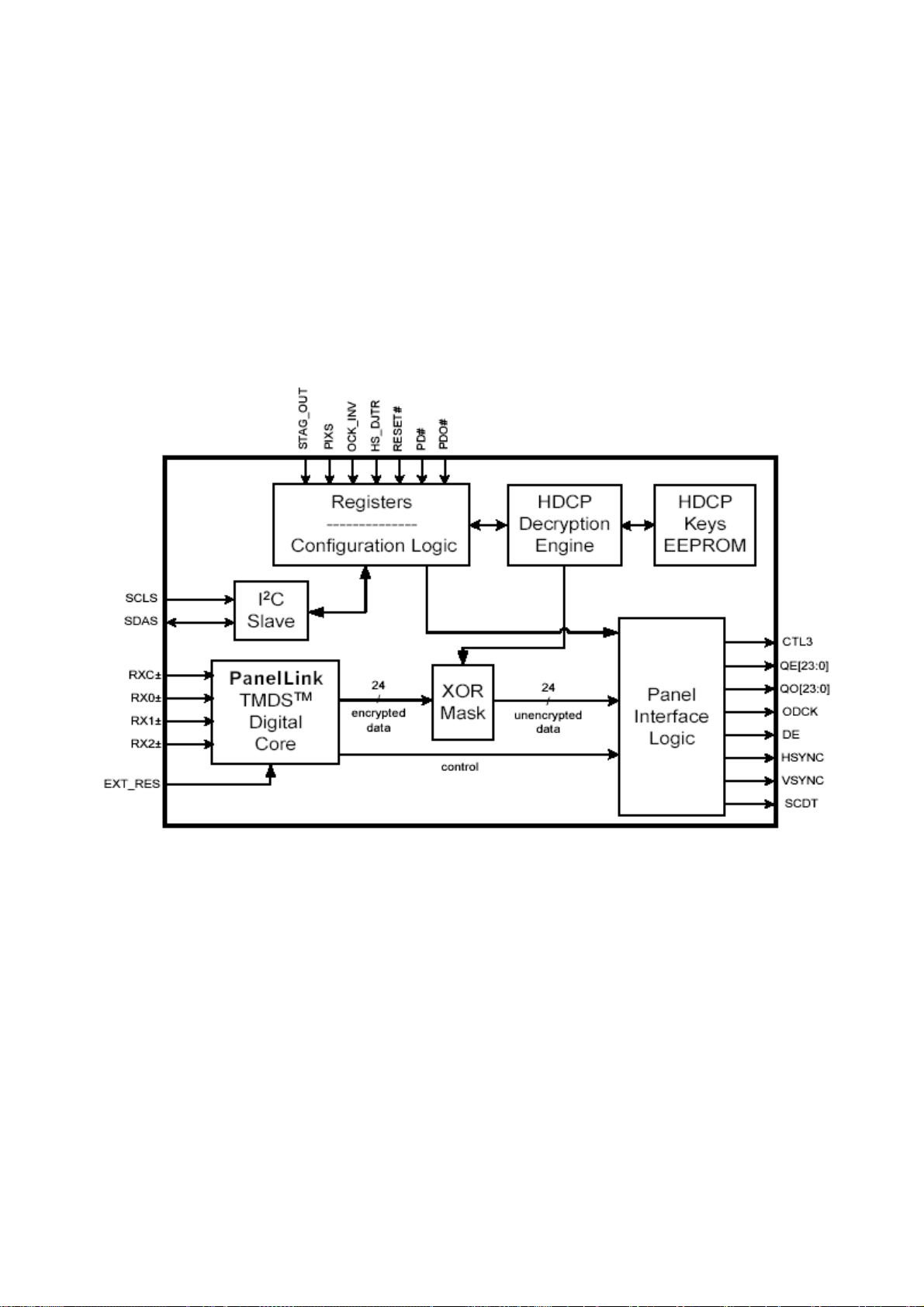
the functional blocks of the chip .
Panel Link TMDS Core
The Panel Link TMDS core accepts as inputs the three TMDS differential data lines and the
differential clock. The core senses the signals on the link and properly decodes them providing
accurate pixel data. The core outputs the necessary sync signals (HSYNC, VSYNC), clock (ODCK),
and a display enable (DE) signal that drives high when video pixel data is present. The SCDT signal
is output when there is active video on the DVI link and the PLL has locked on to the video. SCDT
can be used to trigger external circuitry, indicating that an active video signal is present; or used to
place the device outputs in power down when no signal is present (by tying SCDT to PDO#). A
resistor tied to the EXT_RES pin is used for impedance matching.
CONFIDENTIAL – DO NOT COPY
File No. SG-0156
Page 8-5
Page 27

HDCP Keys EEPROM
The SiI 169 comes pre-programmed with a production set of HDCP keys in its internal EEPROM. In
this way the keys are provided the highest level of protection as required by the HDCP specification.
Silicon Image manages all aspects of the key purchasing and programming. There is no need for the
customer to purchase HDCP keys from the licensing authority. For security reasons, the keys cannot
be read out of the device.
Samples of the SiI 169 are available with the B1 public keys as listed in the back of the HDCP
specification. These are marked with a -PUB part number as noted in the Ordering Information
section. Make sure to request either “Public” or “Production” keys when requesting samples. Before
receiving samples of the SiI 169 with production keys a customer must have signed the HDCP
license agreement.
HDCP Operation
The SiI 169 supports High-bandwidth Digital Content Protection (HDCP) by decrypting the pixel data
stream received from an HDCP transmitter in the video host system. HDCP provides a secure
method of delivering high definition content between a host (such as a set-top box, DVD player, or
D-VHS player) and display (such as an HDTV, projector, or A/V receiver).
The authentication process involves exchanging calculated values based on the keys and KSV. A
software driver running on the host controls the exchange of these values between the host
transmitter (SiI 170B) and the receiver (SiI 169) in the display device. The KSV and two other values,
An and Ri, are exchanged over the DDC channel (I2C bus) of DVI. The receiver is a slave on this
I2C bus. Figure 14 shows a typical HDCP system configuration.
CONFIDENTIAL – DO NOT COPY
Page 8-6
File No. SG-0156
Page 28

The operation of PW66B
The PW166B is highly integrated “System on a chip“ that interfaces computer graphics and video
inputs in virtually any format to a fixed frequency flat panel display. An embedded DRAM frame
buffer and memory controller perform from rate conversion. Computer images from VGA to UXGA
resolution input to the chip can be resized to fit on the target display device. The on chip
microprocessor incorporates with frame buffer, resizing circuitry and peripheral circuit should
supports the features that is frame rate conversion, image scaling, automatic image optimization,
picture in picture, on screen display and user adjustment.
The internal block diagram of PW166B is as follows:
CONFIDENTIAL – DO NOT COPY
Page 8-7
File No. SG-0156
Page 29

The interface of Pw166B is composed by three parts that is microprocessor interface, graphics port
and display port.
Microprocessor interface
When power is supplied and power key is pressed then the reset circuit lets RESET to high state that
will reset the PW166B to initial state. After that the RESET will transits to low state and the PW166B
start to work that microprocessor executes the programs and configures the internal registers. The
PW166B uses two internal PLLs to generate the memory and display clocks, both MCLK and DCLK
are generated from a reference clock input to pin XTALIN according to the following formulas.
FVCOM = XTALIN * (MPLLM+1) / (MPLLN+1)
FVCOD = XTALIN * (DPLLM+1) / (DPLLN+1) Where:
MCLK = FVCOM / 2 ^ MPLLP 250MHz < FVCOM < 550 MHz
DCLK = FVCOD / 2 ^ DPLLP 250MHz < FVCOD < 550 MHz
Valid values for registers MPLLM [7:0] and DPLLM [7:0] are between 0x27 and 0xFF. MPLLN [5:0]
and DPLLN [5:0] are valid from 0x00 to 0x3F. MPLLP [2:0] and DPLLP [2:0] are valid from 0x00 to
0x07. For lower power modes, do not slow the internal PLLs. Instead, use the power control bits
described in Power Saving Modes configured as follows:
CONFIDENTIAL – DO NOT COPY
File No. SG-0156
Page 8-8
Page 30

The GPIO block incorporates two 8-bit general-purpose I/O ports. Each bit in each port is individually
controllable as either input or output.
The three ports are configured as follows:
Pin name Function Type Description
PORTA0 SDA Input / Output I2C SDA
PORTA1 SCL Input / Output I2C SCL
PORTA2 VPCON Output Control LED (Green/Blue) and Main board Power on/off
PORTA3 ADCEN Output AD9883 SOGOUT Enable
PORTA4 PDPON Output Panel power on/off
PORTA5 1231_SCL Input / Output I2C SCL
PORTA6 INSEL Output Select Input signal
PORTA7 PWM Output
PORTB0 15K_DET Input Detect 480i / 480P
PORTB1 DE_MARVSN Output Enable or disable Marco vision
Panel Bright control
PORTB2 MUTE Output Audio mute on/off
PORTB3 DVI_ON Output DVI to Sil169 Enable
PORTB4 COMP_SEL Output YPbPr and DVD switch
PORTB5 1231_En Output GFBK out on/off
PORTB6 So X Not use
PORTB7 1231_SDA Input / Output I2C SCL
CONFIDENTIAL – DO NOT COPY
Page 8-9
File No. SG-0156
Page 31

Graphics port
The graphics port (Gport) is an input interface for high speed RGB data (up to UXGA). It accepts
incoming data at one or two pixels per clock. The GPort can input data at rates up to 236
MPixels/second. It also has sync separator circuitry; timing signals for PLL control, and clock
buffering and conditioning circuitry. The graphics port has three input sources that is from analog
port digital and de-interlace. The data cannot exist simultaneously to avoid interference with each
other and that is controlled through INSEL COMP_SEL, INSEL and DVI_ON.
The block diagram of graphics port is as follows:
The sync decoder detects and processes the horizontal sync (GHS), vertical sync (GVS), sync on
green (GPENSOUT), and field (GFIELD) inputs used for timing. There are several bits to indicate the
status of the inputs. For horizontal sync, HSOK=1 indicates that the horizontal line rate is faster than
10KHz. For vertical sync, VSOK=1 indicates that the vertical field or frame rate is faster than
10Hz .For sync on green, SOGACT=1 indicates that transitions on GPENSOUT are occurring faster
than 10Hz. The PLL control block generates the timing signals required for an external PLL.
GCOAST is an output used to tell the PLL to coast during vertical blanking. This is used to keep the
PLL from making spurious change due to extra or missing HSYNC pulses. Output GREF is a polarity
corrected delayed version of the active horizontal sync signal. GREF is delayed from the input
HSYNC by an amount specified by register PHASE (7:0). Changing PHASE will change the set up
/hold time relationship between the sample clock and the data coming into the external ADC.
CONFIDENTIAL – DO NOT COPY
File No. SG-0156
Page 8-10
Page 32

Output GHSFOUT is the field output signal used to tell an external ADC whether even or odd pixels
are being captured during half sample mode.
When EXTFCE=1 the external flow control is enabled, each new line is marked by an edge on the
GLAVIN input (pin GFBK), but while EXTFCE=0 the GFBKIN input (pin GFBK) is used as the input
HSYNC signal for pixel counters.
Display port
The display port processes and prepares the data for display. The output data is sent out on pins
DRE (7:0), DGE (7:0), DBE (7:0), RRO (7:0), RGO (7:0) and RBO (7:0) that is controlled by display
timing generator.
The block diagram of display port is as follows:
The on screen display data can be merged into the data, as the data is output to the display here.
The on screen display data can also be added as the data is input to the video port, or as data is
input to the graphics port.
The gain function is applied to every pixel .It has the same form as the overlay functions. Specially,
the pixels are processed as follows:
Output red pixel = ((input red pixel) * RCONT (7:0) / 128) + RBRITE (7:0)
Output green pixel = ((input green pixel) * GCONT (7:0) / 128) + GBRITE (7:0)
Output blue pixel = ((input blue pixel) * BCONT (7:0) / 128) + GBRITE (7:0)
CONFIDENTIAL – DO NOT COPY
File No. SG-0156
Page 8-11
Page 33

Where:
CONT should be set to 0x80 for normal operation.
The registers xCONT (7:0) are unsigned values between 0 and 255.
The registers xBRITE (7:0) are signed values between –128 and +127, where 0x00 = 0.
The color look up table replaces each input pixel with a new value based on register tables stored in
the PW166B. This function is used to compensate the inherent gammas of the display device and
the data source. It uses piece-wise linear function to get the output value.
The color space expander allows up to all of the 10 bits per pixel coming from the color look up table
to be used to create as many gray shades as possible on the display device. The color space
expansion is performed using Frame Rate Modulation (FRM) and Dithering. Dithering is performed
before FRM.
The de-multiplexer registers the display pixels before they output to the display. The pixels can also
be set to zero here, or set to default value. The de-multiplexer can support one pixel per clock or two
pixels per clock mode. On one pixel mode the data is sent out on pins DRE97:0), DGE (7:0) and
DBE (7:0) every DCLK. But two pixels mode the data is sent out that even pixels on pins DRE (7:0),
DGE (7:0), and DBE (7:0) and odd pixels on pins RRO (7:0), RGO (7:0), and RBO (7:0).
The PW166B generates the vertical and horizontal timing signals for the display device, and internal
timing signals for the display port portion of the PW166B. The DHS and VHS output signals can be
active high or low, depending on the HSPOL and VSPOL bits. Similarly, DENPOL controls the
polarity of the DENR, DENG and DENB outputs. The DDEN bit enables the DHS, DVS, DENR,
DENG and DENB outputs. The horizontal counter starts with the leading edge of horizontal sync. All
horizontal timing is referred to this edge.
Video Port
The Video Port (VPort) is an input interface for video data. It accepts incoming data in YUV and RGB
formats, and supports picture-in-picture when both the VPort and the GPort are enabled
simultaneously. The VPort can input data at rates up to 75 MPixels/second. Setting bit CAPEN to 0
can disable the Video Port. The block diagram is as follows:
CONFIDENTIAL – DO NOT COPY
Page 8-12
File No. SG-0156
Page 34

The operation of FLI2310
The FLI2310 is a highly integrated digital video format converter for LCD-TV applications using
patented de-interlacing and post processing algorithms from Faroudja Laboratories, coupled with
highly flexible scaling, a wide variety of aspect ratio conversions, and other special video enhancing
features to produce the highest quality image.
The internal block diagram of FLI2310 is as follows:
CONFIDENTIAL – DO NOT COPY
Page 8-13
File No. SG-0156
Page 35

Input Processor
Two input digital data ports are available, each with separate sync and clock signal inputs. Port 1 is a
24-bit data port that accepts the following input formats
24-bit RGB data
24-bit 4:4:4 Y Cr Cb data
24-bit 4:4:4Y Pr Pb data
16-bit 4:2:2 Y Cr/Cb data
16-bit 4:2:2 Y Pr/Pb data
8-bit Y/Cr/Cb data
8-bit Y/Pr/Pb data
8-bit Y/Cr/Cb data with embedded sync, ITU-R BT656 (D1) format
Port 1 has two sets of control inputs – H Sync or Ref, V Sync or Ref, Odd/Even Field identification
and Data clock inputs. Either of the two sets of control input signals can be selected for Port 1 data.
Port 2 in the SHD-3010 we not use.
The data is sampled at the rising edge of the input data clock. The H and V timing control inputs can
be either Sync type signal or Reference (Ref) type signal. Ref signals change logic state between
active video region and inactive blanking region. The polarity of the input H and V control signals is
also programmable. An Odd/Even Field identifier signal input is provided, but this is not required
when the control inputs are syncs as it is generated within the chip in this case. The polarity of the
external Odd/Even Field identifier is also programmable.
For SHD-3010 we use ITU-R BT656 the ITU-R BT656 signals with embedded timing, the Ref signals
are constructed from EAV (End of Active Video) and SAV (Start of Active Video) blocks.
CONFIDENTIAL – DO NOT COPY
Page 8-14
File No. SG-0156
Page 36

SDRAM
The SDRAM types used with the FLI2310 should be organized as 32-bit wide SDRAM (i.e. one 2M x
32-bit) controller, up to 166 MHz operations, for external SDRAM
The built-in SDRAM interface (SDI) controls the access to the SDRAM for the de-interlace and the
frame rate converter. Multiple read channels are used for the de-interlace. An arbitrator controls the
write and read operations based on the status of the FIFOs present at each read and write channel,
ensuring that underflow of FIFOs do not occur. Adequate depth of the FIFOs ensures that no
overflow occurs. 4MB of SDRAM memory is required for full functionality of the chip. The SDI
supports use of one 2M x 32 SDRAM. The SDI supports SDRAM operation speeds up to 166MHz.
The SDRAM speed grade required is application-dependent. To enable all the possible format
conversions, usage of a 166 MHz SDRAM is advised.
SDRAM Interface Block Diagram
Pin name Function Type Description
CLK 23SDCLK Input SDRAM clock.
MCLKFB VIDMFB Input SDRAM clock feedback
/RAS 23SDRAS Output SDRAM row address strobe
/CAS 23SDCAS Output SDRAM column address strobe
/WE 23SDWEN Output SDRAM write enable
SDRAM Compatible Devices
CONFIDENTIAL – DO NOT COPY
Page 8-15
File No. SG-0156
Page 37

Noise Reducer
A motion adaptive frame based recursive noise reduction is performed on both chroma and luma
data. The external SDRAM frame memory is used for this purpose. An innovative noise meter
measures the amount of noise in the picture. The noise measurement is done within the active video
region, and not in the blanking region. This eliminates the possibility of wrong noise measurement
due to the clamping normally done during blanking period by analog to digital converters.
The degree of sensitivity to motion is programmable. Depending on the degree of noise present and
motion sensitivity defined, the recursive filter values are selected. Facial features may be adversely
affected if the noise reduction done on such areas uses the recursive filter levels optimized for the
overall picture. To prevent this and to provide a more natural picture, flesh tones are identified and
during the presence of flesh tones, the noise reduction algorithm is modified. Noise reduction is done
only on standard definition PAL and NTSC inputs.
Microprocessor Interface
A standard 2-wire, serial interface enables convenient register control. All the blocks are fully
programmable. The device address of the chip is programmed with the hardware settings of the
DEV_ADDR 1 and DEV_ADDR 0 pins, preventing conflict with the other devices connected to the
bus. The slave address can be set to any of the following values:
The operation of VPC3230D
The VPC3230D is a high-quality, single-chip video front-end, which is targeted for 4:3 and 16:9,
50/60 and 100/120 HZ TV sets. It can be combined with other members of the Digit3000 IC family
And/or it can be used with 3
rd
-part products.
CONFIDENTIAL – DO NOT COPY
Page 8-16
File No. SG-0156
Page 38

Input port
This chip has five analog input port and mainly carries out analog- to-digital conversion
for the following digital video processing. These input port are clamped to the sync back porch and
are amplified by a variable gain amplifier. One input is for connection of S-VHS carrier-chrominance
signal. Four inputs are for composite video or S-VHS luma signal.
VPC 32xxD provides two analog RGB/YCrCb input ports, one with Fast Blank capability and one
without. It is strongly recommended to use analogue 5 MHz anti-alias low-pass filters on each input,
including FB. While all signals need to be capacitively coupled by 220 nF clamping capacitors, the
Fast Blank input requires DC coupling.
input ports are configured as follows:
Pin name Symbol Type Description
Cin 71 Input Sivd-C2
Vin1 72 Input Svid-Y2
Vin2 73 input All
Vin3 74 Input All
Vin4 75 input Y-COMP
FB1IN 79 Input CC-FSW
B1/CB1IN 1 Input CC-B
G1/Y1IN 2 Input CC-G
R1/CR1IN 3 Input CC-R
B2/CB2IN 4 Input B-COMP
G2/Y2IN 5 Input Y-COMP
B2/CB2IN 6 Input R-COMP
CONFIDENTIAL – DO NOT COPY
Page 8-17
File No. SG-0156
Page 39

Color decoder
The standard luma/chroma separation and multi-standard color demodulation is carried out.
The color demodulation uses an asynchronous clock, thus allowing a unified architecture for all color
standards. The color decoder also provides several special modes, wide band chroma format, which
is intended for S- VHS wide bandwidth chroma. Also, filter settings are available for processing a
PAL+ helper signal.
A block diagram of the color decoder as follows
Output port & ITU-R 656 Output Format
This interface uses an YcrCb 4:2:2 data stream at a line-locked clock of 13.5 MHz. Luminance and
chrominance information is multiplexed to 27 MHz in the following order:
Cb1, Y1, Cr1, Y2,
Timing reference codes are inserted into the data stream at the beginning and the end of each video
line:
—A ‘Start of active video’-Header (SAV) is inserted before the first active video sample
—A ‘End of active video’-code (EAV) is inserted after the last active video sample.
For activation of this output format, the following selections must be assured:
– 13.5 MHz line locked clock
– Double-clock mode enabled
– ITU-R656-mode enabled
– Binary offset for Cr/Cb data
CONFIDENTIAL – DO NOT COPY
Page 8-18
File No. SG-0156
Page 40

All data and sync pins operate at TTL compliant levels and can be tristated via I2C registers.
Additionally, the data outputs can be tristated via the YCOE output enable pin immediately. This
function allows the digital insertion of a 2nd digital video source To minimize crosstalk data and clock
pins automatically adopt the output driver strength depending on their specific external load (max.
50pF). Sync and FIFO control pins have to be adjusted manually via an I2C register.
output ports are configured as follows:
Pin name Symbol Type Description
Y0 40 Output VID_Y0
Y1 39 Output VID_Y1
Y2 38 Output VID_Y2
Y3 37 Output VID_Y3
Y4 34 Output VID_Y4
Y5 33 Output VID_Y5
Y6 32 Output VID_Y6
Y7 31 Output VID_Y7
C0 50 Output VID_UV0
C1 49 Output VID_UV1
C2 48 Output VID_UV2
C3 47 Output VID_UV3
C4 44 Output VID_UV4
C5 43 Output VID_UV5
C6 42 Output VID_UV6
C7 41 Output VID_UV7
The operation of SAA7118
The SAA7118 is a video capture device for applications at the image port of VGA controllers.
SAA7118 also provides a means for capturing the serially coded data in the vertical blanking interval
(VBI-data). Two principal functions are available:
1. To capture raw video samples, after interpolation to the required output data rate, via the
scaler.
2. A versatile data slicer (data recovery) unit.
The SAA7118 also incorporates field-locked audio clock generation. The function ensures that
there is always the same number of audio samples associated with a field, or a set of fields. This
prevents the loss of synchronization between video and audio during capture or playback. The
function block diagram as follows:
CONFIDENTIAL – DO NOT COPY
Page 8-19
File No. SG-0156
Page 41

Analog input processing
The SAA7118 offers sixteen analog signal inputs, four analog main channels with source switch,
clamp circuit, analog amplifier, anti alias filter and video 9-bit CMOS ADC.
The analog input ports are configured as follows:
Pin name Symbol Type Description
K2 AI13 Input Pip mode Input
L3 AI14 Input S-Video Y2
G4 AI21 Input Y_CMP1 Input
G3 AI22 Input Y_CMP2 Input
J3 AI24 Input S-Video C2
E3 AI31 Input B_CMP1 Input
F2 AI32 Input B_CMP2 Input
F3 AI33 Input Tv2 _CVBS Input
B1 AI41 Input R_CMP1 Input
D2 AI42 Input R_CMP2 Input
E1 AI44 Input CVBS_PIP Input
N4 CE Input RST_Video
CONFIDENTIAL – DO NOT COPY
Page 8-20
File No. SG-0156
Page 42

The function Analog input process diagram as follows:
Chrominance and luminance path
Chrominance path
The 9-bit CVBS or chrominance input signal is fed to the input of a quadrate demodulator,
Where it is multiplied by two time multiplexed sub carrier signals from the sub carrier generation
block (0°and 90° phase relationship to the demodulator axis). The frequency is dependent on the
chosen color standard.
The chrominance low-pass 1 characteristic also influences the grade of cross-luminance reduction
during horizontal color transient (large chrominance bandwidth means strong suppressing of
cross-luminance). If the Y-comb filter is disable by YCOMB=0 the filter influences directly the width of
the chrominance notch within the luminance path (a large chrominance bandwidth means wide
chrominance notch resulting in a lower luminance bandwidth).
CONFIDENTIAL – DO NOT COPY
Page 8-21
File No. SG-0156
Page 43

Luminance path
The rejection of the chrominance components with the 9-bit CVBS or Y input signal is achieved by
subtracting the demodulated chrominance signal from the CVBS input.
The comb filtered C
components are interpolated (up sampled) by the low pass 3 block
B-CR
It’s characteristic is controlled by LUBW (sub address 09H, bit4) to modify the width of the
chrominance ‘notch’ without influencing the width of the chrominance ‘notch’ without influencing the
chrominance path.
The function Chrominance and Luminance diagram as follows:
CONFIDENTIAL – DO NOT COPY
Page 8-22
File No. SG-0156
Page 44

Decoder output formatter
The output interface block of the decoder part contains the ITU656 formatter for the expansion
port data output XPD7 to XPD0 and the control circuit for the signals needed for the internal paths to
the scaler and data slicer part. It also controls the selection pf scaler and data slicer part. It also
controls the selection of the reference signals for the RT port and the expansion port.
The generation of decoder data type control signals SET_RAW and SET_VBI is also done
within this block. These signals are decoded from the requested data type for the scaler input and/or
the data slicer, selectable by the control registers LCR2 to LCR24
Data formats at decoder output
Data type number Data type Decoder output data format
0 Teletext EuroWST, CCST Raw
1 European closed caption Raw
2 Video Programming service Raw
3 Wide screen signal bits Raw
4 US teletext (WST) Raw
5 US closed caption Raw
6 Video component signal, VBI region Y-CB-CR 4:2:2
7 CVBS data Raw
8 Teletext Raw
9 VITC/EBU time codes (Europe) Raw
10 VITC/SMPTE time code (USA) Raw
11 Reserved Raw
12 US NABTS Raw
13 MOJI(Japanese) Raw
14 Japanese format switch(L20/22) Raw`
15 Video component signal, active video region Y-CB-CR 4:2:2
The operation of TA1218F
The TA1218N/F is an audio/video switching IC for TV sets. Conforming to I2C bus standards, it
allows you to perform various switching operations through the bus lines by using a microcomputer.
Thanks to its 2-channel outputs, the TA1218N/F can also be used for the PIP systems. Furthermore,
since the presence of a signal on its sync signal output pin can be determined by a microcomputer, it
is possible to check each input/output channel (self-diagnosis). This IC has the same pin
assignments as the TA1219AN (SDIP36), a 1-channel output version of the TA1218N/F.
CONFIDENTIAL – DO NOT COPY
File No. SG-0156
Page 8-23
Page 45

TA1218F block diagram
Operation of power board description
Figure 1 shows a schematic of the double forward converter construction and boost converter
construction..
Figure 2 shows a schematic of the fly back converter structure.
Fly back converter topology is shown in Fig 2.Referring it Fig 2 , the topology works as follows.
During their power MosFet on times , they store energy in their power transformer while load current
is supplied from an output filter capacitor . When the power MosFet turns off, the energy stored in the
power transformer is transferred to the output as load current and to the filter capacitor to replenish
the charge it lost when it alone was delivering load current.
CONFIDENTIAL – DO NOT COPY
File No. SG-0156
Page 8-24
Page 46

When AC voltage through D1 diode into the B point. The B point voltage is AC voltage * √2 (Vb) .
The Vb around resistors R56 and R59 of figure 2 into the pin3 of U5 (SG6841) via pin7 to charge
C50. When across the voltage of C50 reaches 16Vdc, the U5 start operating.
Once U5 operation, the Pin8 of the U5 will yield a square waveform of 50KHz frequency to switching
Q10 (Power MosFET) result in power transformer T3 (PQ2625) stored energy during Q10 on time
and delivered energy during Q10 off time. When Q10 turned off will yield biased voltage due to
biased winding. The biased voltage provides a steady voltage to charge C50 capacitor after via
rectifier diode D14, in order to make U5 (SG6841) continue operation. Once power transformer T3
start delivering energy to secondary, the secondary will yield a DC voltage to output after via rectifier
diode D11 and π-type filter of capacitor C46 and inductor L4 and capacitor C47. The V (K-A) of the
U7 from high voltage slowly decreases to closely steady voltage when output slowly increases.
Simultaneously, the slightly current follows Pin(1-2) of the photocopier U6 and Pin(3-4) of the linear
regulator U7 after output voltage is sensed by sampling resistors R66 and R70 and compared to a
reference voltage Vref (〜2.5Vdc) in the reference point (Pin1) of the U7. Due to Pin2 of the U5 vary
versus current amplitude that follow Pin (1-2) of the U6. The Pin2 of the U5 is fed to a
pulse-width-modulator (PWM) to control duty-cycle with comparator to Pin6 of the U5 so that make
output voltage steady.
PFC converter topology is shown in Fig 1.Referring it Fig 1, the topology works as follows. When Q1
turns on off the polarity across L1 reverse, and the dot end (A point of L1) rises to a voltage (B point)
higher than the input voltage (Vin). Energy stored in L1 during Ton is transferred via D2 to the load
and C4 during the Q1 off time.
Another, the steady biased voltage also to charge capacitors C22 and C19 as across them voltage
reaches 13Vdc, the IC1 (CM6800-1) continue operation when Pin C of the CN1 and CN3 is a high
signal (+5V). Once IC1 operation, the Pin12 of the IC1 will yield a square waveform of about 69KHz
frequency to switching Q1 (Power MosFet) and cause L1 start storage energy during Q1 on time and
deliver energy during Q1 off time. It can be shown that the output-input voltage relation of such a
boost converter is given by
Vin
Vo( B point) = ( Eq 1.1)
1 Ton / T
CONFIDENTIAL – DO NOT COPY
Page 8-25
File No. SG-0156
Page 47

Now throughout the half sinusoids of Vin, the Q1 on time, denoted by Ton, is width-modulated in
accordance with Eq. 1.1 to yield a constant DC voltage Vo( B point ) is about 380Vdc somewhat
higher than the peak of input voltage sine wave. The on time throughout the sinusoidal half periods is
controlled by a PFC control chip(IC1) which senses Vo (B point) via R3 and R14 resistor , compares
it to an internal reference in a DC voltage error amplifier ( Pin15 of IC1) , and in a negative feedback
loop (Pin 3 of the IC1) sets Ton to keep Vo constant at the selected value.
When Vo reaches 380Vdc, the FB point (Pin 15 of IC1) is closely 2.5Vdc. It will drive PWM section of
the IC1.
The double-ended forward converter works as follows. In Fig 1, Q3 and Q4 are in series with the top
and bottom of the transformer primary. Both of this power Mosfet close are turned on simultaneously
and turned off simultaneously. When they are on, all primary and secondary dot ends (Pin2 of the T1)
are positive and power is delivered to the loads. When they turn off, current stored in the T1
magnetizing inductance reverses polarity of all windings. The dot end of Np tries to go far negative
but is caught at ground by diode D7. The no-dot end of Np tries to go far positive but is caught at Vdc
by diode D4. Thus the emitter of Q3 can never be more than Vdc below its collector, and the collector
of Q4 can never be more than Vdc above its emitter. Now the pin11 point of the IC1 will yield a
square waveform of 69KHz frequency to switching Q3 and Q4 and cause T1 start storage energy
during Q3 and Q4 on time and deliver energy during Q3 and Q4 off time. When Q3 and Q4 is turned
on , the dot end of the primary power winding Np and secondary go positive with respect to no dot
end. Current and power flows into the dot end of Np. Rectifier diode D3 are forward-biased and
current power flows output of the dot end of secondary to the LC filters (L2, C8, C9, L3.C10) and the
load. Diode D3 act like the freewheeling diode at Q3 and Q4 turn off. Duty-cycle is controlled by Pin6
with compared to pin8. Pin6 voltage is selected by U3 and U2.
OVP function is controlled by ZD2 and ZD8 to sense output (+12V and +24V). When output voltage
is over the clamp voltage of ZD2 and ZD8, ZD2 and ZD8 is turned on to driving Q2 result in Q2 turn
on cause U8 have large current flows in to the base of the Q12 result in Pin5 of the U1 and Pin 2 and
Pin7of the U5 immediately down to zero to default power supply.
Power saving function is controlled by Pin C of CN1 and CN3 . When Pin C is low signal , Q5 is
turned off result in U4 keep off stage cause Q7 not turn on result in across on C22 voltage not
delivered to the Pin 13 of the IC1 to closed IC1 .
CONFIDENTIAL – DO NOT COPY
Page 8-26
File No. SG-0156
Page 48

Keep L,N,SG trace for 3mm at least.
F1
C6
C13
0.0022UF/250V
R39 47
R40 75K
R48
13K
2R5 OHM 6A
R8 1M(1/2W)
10D/471K
VZ1
+
C37
C29
1uF
50V
0.1uF
5A/250V(Time-Lag)
CN2
5P 3.96
L
1
0.0022UF/250V
2
3
SG
4
5
N
3
1
2
U1-PIN5(2)
10
C28
0.47u
63V
D1
PS206
1 2
D2
Q1
B,C
C2
C12
C32
0.1u
100V
LF2
ET24C
C18
220pF
1KV/Y5P
D8
1N4002
D9
1N4002
R35
13K
1
2
3
4
5
6
7
8 9
R49
C40
470PF
(NPO)
U1
CM6800-1
R46
47K
NC
C24
NC
0.0022UF/250V
C7
C14
0.0022UF/250V
R19
0.3R
2W
1 2
1 2
220pF(NPO)
C25
2n2/100V
C41
1000P
50V
10D/471K
-+
4
VZ2
R26
0.3R
2W
16
15
14
13
12
11
10
ZD6
1 2
BD1
GBU6J
2
R4
412K
1
1/4W
C16
3
R15
0.68uF
400V
412K
MKP
1/4W
R34
60.4K
R421
R43
1
ZD7
C38
1uF
1 2
50V
HZ22-2
HZ22-2
NT1
LF1
ET24C
C11
NC
0.47uF/275Vac
C30
C31
1000P
470PF
(NPO)
L1
short
A D
R5
475K
1/4W
12
R9
22R
D5
R16
1/4W
1N4148
475K
1/4W
D21
SB140
12
C19
100uF
25V
9
4 8
1
6
3
7
10
2
C
R33
3K3
ZD4
HZ20-2
1 2
+
+
C34
C33
0.1uF
0.01u
C39
1uF
50V
8ETH06
22N50A
500V/22A
1 2
23
R2
R6
1
200R
200R
2W
2W
C15
220pF
1KV/Y5P
C18
R18
220pF
10K
1KV/Y5P
1/4W
Q6 2SA673P
R17
10K
Q7
2SC1213
ZD5
R29
10K
7B2
R51
1K
R37 182K
R44
1.3K
C35
R50
1000P
7K5
B (2)
C4
150uF
450V
C5
+
NC
30x30
R14
475k
1/4W
T2
EE-13
259
R20
4R7
1/4W
C20
0.47uF
63V
R10
+
C22
10k
10U/50V
R24
2
33K
1 3
+
C23
10u
50V
7
4
6
8
9
R47
620K
C36
0.01uF
C42
0.1uF
Q3
2SK3520
500V/9A
23
R12
R3
475K
10K
D4
1/4W
1/4W
1
PG108R
R11
22R
1/4W
C17
0.1uF
100V
7
R21
22R
1/4W
A (2)
1A/800V
ZD1
HZ22-2
2
4
D7
PG108R
6
23
Q4
2SK3520
1
500V/9A
R27
10k
1/4W
R22
1.2
1WS
7
R23
1.2
1WS
VDD(2)
43
43
T1
EER35C
1 2
C21
332/250V
U2
TLP621GR
U4
TLP621GR
13
14
10,11,12
1
2
1
2
C1
222P
500V
2 1
2SC1213
30CPQ100
TO247
ZD10
20-2
3
U3
TL431
R53
1K
Q5
C55
R1
222P
33
1WS
500V
D3
1 3
R52
10K
R45
10K
R38
39K
2
Q8
2SC1213
ZD3
6B1
C3
222P
500V
C53
222P
500V
R13
33
1WS
2
1 3
1,3 2,4
24V
R81
20K
2
Q9
2SC1213
1 3
R32
3.3K
1/4W
C26
NC
C27
333PF
12V
2
L2
81uH
Q13
2SC1213
1 3
R54
R30
NC
2.7K
R28
5.1K
+
C54
NC
C8
1000uF
35V
12.5Dx25
L3
6 x 25
1 2
+
C9
NC
+
C57
2.2uF
50V
CN4
NC
1
2
R57
NC
R27
3.6K
R7
NC
1/4W
R36
19.6K
1/4W
R41
2.26K
CN1 CN3
TO INVERTER(24V)
15
14
13
12
11
10
9
8
7
+
C10
6
470u
5
35V
4
10DX20
3
2
1
D (2)
C (2)
F (2)
1
GND
2
FB
3
VIN
4 5
RI RT
R69
33K
Fosc=50KHz
U5SG6841
8
GATE
7
VDD
6
SENSE
R78
NC
Secondary GND
Primary GND
Figure 1
P6KE150A
R55
0.22 2W
B(1)
D6
1N4148
R61
10
1/4W
R56
750K
1/4W
R59
750K
1/4W
12
C56
470P/50V
A(1)
VDD(1)
Q11
2SA1015
TO-92
U1-PIN5(1)
C(1)
D16
2SK3677
T0-220F
Heat Sink
R72
10K
1
3
12
C51
0.1uF
P=5mm
UF4006G
DO-41
Q10
R31
120
C43
0.1uF
R73
100K
2
D20
1N4148
1 2
P6KE150A
D17
D12
1
2
R76
100K
T3
PQ2625
4
4
11,12
7,8
U6
PC-621
U8
PC-621
R58
33 1WS
1
3 2
D11 FCH20A15
Heat Sink
1
23
12V
1
23
2
R80
1 3
1K
C49
222P/500V
R67
820
1/4W
R79
1K
1 2
R75
NC
Q2
2SC1213
1 2
C45
222P/500V
JP1
JP2
L4
1 2
5.8uH/5A
P=10mm
C46
+
1000u
25V
(KY)
12.5*20 12.5*20
R74
330
R25
330
+
C47
470u
25V
(KY)
TL431
TO-92
12B2 1/2W
R65
3.3K
1/4W
C48
223PF
U7
3
2 1
R66
R60
9.53K
NC
R68
10K
R70
2.49K
ZD8
ZD2
24-3
C44
1
2n2/1KV
P=5mm
2
3
R71
1K
1/4W
Q12
2SC1815
TO-92
D13
UF4003G
R63
3.3
1/4W
C50
10uF
50V
(KY)
5*11
4
5
D14
UF4003G
R64
4.7
1/4W
+
12
D15
1N4148
ZD9
24-2
1 2
23
R62
0.24
1WS
1 3
W2
TO MAIN BD(12V)
1
2
3
4
5
6
7
8
C (1)
D (1)
F (1)
CONFIDENTIAL – DO NOT COPY
R77
1K
Figure 2
Page 8-27
File No. SG-0156
Page 49

System Block Diagram
Vb
AC Input
EMI
filiter
Detect Iac/Vrms
Full bridge
rectifier
Inductor
store&
deliver
energy
PowerMosFe
t switching
Buck
capacitor
filter
FORWARD
PFC/PWM control
Feedback
control
Vb
Power MosFet
switching
Transformer
Transfer energy
Diode
Retifiler
Inductor
Store and
deliver
energy
24Vo
Power Mosfet
switching
Inductor/ capacitor
filter
12Vo
Transformer
store& deliver
energy
Diode
Capacitor
Inductor
Retifiler
filter
Bias voltage
Pin C OFF
FLYBACK
PWM control
Power saving
Forward PFC
PWM Control
12Vo OFF
24Vo
CONFIDENTIAL – DO NOT COPY
OVP Proction
fuction
All controllers`
Page 8-28
File No. SG-0156
Page 50

Chapter 9 Waveforms
PC Analog Mode 1024×768 75 HZ
CH1 H-sync (U1 pin7); CH2 V-sync (U1 pin8)
G-BUF (U1 pin4); CH2 V-sync (U1 pin8)
CONFIDENTIAL – DO NOT COPY
Page 9-1
File No. SG-0156
Page 51

CH1 HSYNC-SW (U6 pin30) ; CH2 VSYNC-SW (U6 pin31)
CH1 GCOST (U6 pin 29)
CH1 GBLKSPL (U6 pin 38)
CONFIDENTIAL – DO NOT COPY
Page 9-2
File No. SG-0156
Page 52

CH1 SCL (U6 pin56); CH2 SDA (U6 pin57)
CH1 GCLK (U6 pin67)
CH1 GFBK (U6 pin66); CH2 GVS (U6 pin64)
CONFIDENTIAL – DO NOT COPY
Page 9-3
File No. SG-0156
Page 53

CH1 GFBK (U6 pin66); CH2 GHS (U8 pin8)
CH1 B-SW (U6 pin43)
CH1 GBE (U6 pin19)
CONFIDENTIAL – DO NOT COPY
Page 9-4
File No. SG-0156
Page 54

CH1 (U11 pin P3)
CH1 RST_166(U11 pin E3)
CH1 ROMOEN (U11 pin M1)
CONFIDENTIAL – DO NOT COPY
Page 9-5
File No. SG-0156
Page 55

CH1 DCLK (U11 pin W12)
CH1 DVS (U11 pinV13); CH2 DHS (U11 pinU13)
CH1 BLANK (U11 pin Y15)
CONFIDENTIAL – DO NOT COPY
Page 9-6
File No. SG-0156
Page 56

CH1 DBE (U11 pin Y19)
CH1 A0 (U11 pin P1)
CH1 D0 (U11 pin F4)
CONFIDENTIAL – DO NOT COPY
Page 9-7
File No. SG-0156
Page 57

CH1 TXOUT0 (U21 pin 48)
PC DVI Mode 1024×768 75 HZ
CH1 RXB+(U33 pin81); CH2 RXR+(U33 pin90)
CH1 GHS (U33 pin48); CH2 GVS (U33 pin47)
CONFIDENTIAL – DO NOT COPY
Page 9-8
File No. SG-0156
Page 58

CH1 GFBK (U8 pin3); CH2 GPEN (U33 46)
CH1 GCLK (U33 pin46)
CH1 RP54(U33 pin37); CH2 RP59 (U33 17)
CONFIDENTIAL – DO NOT COPY
Page 9-9
File No. SG-0156
Page 59

CH1 DVS (U11 pinV13); CH2 DHS (U11 pinU13)
CH1 BLANK (U11 pinY15)
CH1 DCLK (U11 pin W12)
CONFIDENTIAL – DO NOT COPY
Page 9-10
File No. SG-0156
Page 60

CH1 DRE (U11 pin R19)
CH1 TXOUT1 (U21 pin 46)
HDTV YPbPr; DVD Mode 480i/480P 480i
CH1 Y_COMP1 (U3 pin 4)
CONFIDENTIAL – DO NOT COPY
Page 9-11
File No. SG-0156
Page 61

CH1 SYNC DET (U3 pin24)
CH1 XTAL1 (U10 pin 62)
CH1 SCL_V (U10 pin 13); CH2 SDA_V (U13 pin 14)
CONFIDENTIAL – DO NOT COPY
Page 9-12
File No. SG-0156
Page 62

CH1 VID_VS (U10 pin 57); CH2 VID_HS (U10 pin 56)
CH1 VID_DATA (U10 pin 53)
CH1 VID_CLK2 (U10 pin 28)
CONFIDENTIAL – DO NOT COPY
Page 9-13
File No. SG-0156
Page 63

CH1 VID Y7 (U10 pin 31); CH2 VID Y0 (U10 pin 40)
CH1 1231_SDA (U19 pin 46); CH2 1231_SCL (U19 pin 45)
CH1 Y4 (U19 pin 191)
CONFIDENTIAL – DO NOT COPY
Page 9-14
File No. SG-0156
Page 64

CH1 GVS (U19 pin 119); CH2 GHS (U19 pin 118)
CH1 GCLK (U19 pin 125)
CH1 23SDCLKI (U19 pin 114)
CONFIDENTIAL – DO NOT COPY
Page 9-15
File No. SG-0156
Page 65

CH1 23SDCS# (U19 pin 109)
CH1 23SDBA0 (U19 pin 108)
CH1 23SDBA1 (U19 pin 107)
CONFIDENTIAL – DO NOT COPY
Page 9-16
File No. SG-0156
Page 66

CH1 23SDCAS# (U19 pin 106)
CH1 23SDRAS# (U19 pin 105)
CH1 GFBK (U8 pin 6)
CONFIDENTIAL – DO NOT COPY
`
Page 9-17
File No. SG-0156
Page 67

CH1 GBE (U19 pin 155)
480P
CH1 Y_COMP1 (U3 pin 4)
CH1 SYNC DET (U3 pin 24)
CONFIDENTIAL – DO NOT COPY
Page 9-18
File No. SG-0156
Page 68

CH1 GFBK (U6 pin 66); CH2 GHS (U8 pin 8)
CH1 GCLK (U6 pin 67)
CH1 GRE (U6 pin 70)
CONFIDENTIAL – DO NOT COPY
Page 9-19
File No. SG-0156
Page 69

CH1 DVS (U11 pin V13); CH2 DHS (U11 pin U13)
CH1 BLANK (U11 pin Y15)
CH1 DCLK (U11 pin W12)
CONFIDENTIAL – DO NOT COPY
Page 9-20
File No. SG-0156
Page 70

CH1 DRE (U11 pin R19)
TV; AV1; AV2/S MODE
CH1 V1 (UT3 pin 38)
CH1 VID_VS (U10 pin 57); CH2 VID_HS (U10 pin 56)
CONFIDENTIAL – DO NOT COPY
Page 9-21
File No. SG-0156
Page 71

CH1 VID_DATA (U10 pin 53)
CH1 VID_CLK2 (U10 pin 27)
CH1 VID_Y7 (U10 pin 31)
CONFIDENTIAL – DO NOT COPY
Page 9-22
File No. SG-0156
Page 72

CH1 GVS (U19 pin 119); CH2 GHS (U19 pin 118)
CH1 DVS (U11 pin V13); CH2 DHS (U11 pin U13)
CH1 DRE (U11 pin R19)
CONFIDENTIAL – DO NOT COPY
Page 9-23
File No. SG-0156
Page 73

POWER ON/OFF
CH1 F1 12DCV/ON
CH1 F1 12DCV/OFF
CH1 F3 V50DC/ON
CONFIDENTIAL – DO NOT COPY
Page 9-24
File No. SG-0156
Page 74

CH1 F3 V50DC/OFF
CH1 F2 V33DC/ON
CH1 F2 V33DC/OFF
CONFIDENTIAL – DO NOT COPY
Page 9-25
File No. SG-0156
Page 75

CH1 LCD_VOL/ON
CH1 LCD_VOL/OFF
CH1 V33_V/ON
CONFIDENTIAL – DO NOT COPY
Page 9-26
File No. SG-0156
Page 76

CH1 V33_V/OFF
CH1 V50_V/ON
CH1 V50_V/OFF
CONFIDENTIAL – DO NOT COPY
Page 9-27
File No. SG-0156
Page 77

CH1 V120V/ON
CH1 V20V/OFF
CONFIDENTIAL – DO NOT COPY
Page 9-28
File No. SG-0156
Page 78

Chapter 10 Trouble shooting
g
MONITOR DISPLAY NOTHING (PC MODE DVI&ANALOG)
Start
LED is lighted
N0
1. Is Power board output
+12V?
2. Is w6 connector good?
3. Is DC-DC OK?
4. Is U11 working ok?
LED is lighting?
Yes
N0
N0
It is in power saving
1. Check video cable
2. Is the timing supported?
3. Check GHS and GVSI
4. Check U6 if analog (SOG)
5. Check U33 If di
ital
Yes
N0
Is backlight on?
1.Check w6
2.Is inverter ok?
Yes
Yes
N0
U11 no data out?
It means data to LVDS
1.Is w5 connected good?
2.Check w5 (V120_V)
3.Check U21 & U11
4.Is panel ok?
Yes
U11 no data in?
N0
It means data from U6 or U33
1.Is U11 working good?
2.Is U33&U6 working good?
1.Check U33 if digital
2.Check power of U33 if digital
3.Check w9 if digital
4.Check U6 if analog
5.Check power of U6 if analog
6.Check w1 if analog
END
CONFIDENTIAL – DO NOT COPY
Page 10-1
File No. SG-0145
Page 79

(TV, VIDEO1, 2, S-VIDEO) IS NOT DISPLAY CORRECTLY
Star t
N0
Input signal is good?
1.Check video
2.Check host’s setting
UT3 input is correct?
U10 input is correct?
U19 input is correct?
U11 input is correct?
LVDS input is correct?
Yes
Yes
Yes
Yes
Yes
N0
N0
N0
N0
N0
1.Check JT5 input if composite
2.Check tuner UT6 PIN12 if TV
mode
3.Check JT8 input if s-video
4.Check signal between UT3 and
JT5 & tuner & JT8
1.Check U10 input
2.Check U10 Power
1.Check U19 input
2.Check U19 power
3.Check UT3 Output
1.Check U11 input
2.Check U11 power
3.Check U10 Output
4.Check U10 Clock
1.Check U11 Output
2.U21 input
3.Check U11&U21power
4.Check U11 Output
Yes
1.Is W5 connected is good?
2.Is panel working ok?
END
CONFIDENTIAL – DO NOT COPY
Page 10-2
File No. SG-0145
Page 80

(DVD, HDTV) IS NOT DISPLAY CORRECTLY
Star t
N0
Input signal is good?
1.Check video
2.Check host’s setting
Yes
U3 input is correct?
Yes
U10 input is correct?
Yes
U19 input is correct?
Yes
U11 input is correct?
Yes
LVDS input is correct?
Yes
N0
N0
N0
N0
N0
1.Check signal between U3 and
JT11 & JT10
2.Check U3 & U1 Input/output
3.Check U3 & U1 Power
1.Check U10 input if 480i
2.Check U10 Power if 480i
3.Check U6 input if 480p
4. Check U6 Power if 480p
1.Check U19 input if 480i
2.Check U19 power if 480i
1.Check U11 input (i480i&480P)
2.Check U11 power (i480i&480P)
1.Check U11 Output
2.U21 input
3.Check U11&U21power
4.Check U11 Output
1.Is W5 connected is good?
2.Is panel working ok?
END
CONFIDENTIAL – DO NOT COPY
Page 10-3
File No. SG-0145
Page 81

TROUBLE OF DC-DC CONVERTER
Star t
W6 PIN1, 2,3 is 12V?
N0
The voltage is about + 12V
1.Check power board
2.Check power cable connection
W6 is good?
U23&U25 Voltage
U27 pin5 is +12V
U29 pin5 is +3.3V
U31 pin5 is +5V
U32 pin5 is +5V
Yes
Yes
Yes
Yes
Yes
N0
N0
N0
N0
N0
The voltage is about + 12V +5V
+3.3V while power plug on
1.W1&W4 to keypad connection is
good?
2.Check U23 is 12V -> 5V
The voltage is about +12V while
power switch on
1.Check U27 pin1 is +12V
2.Check U27 pin 2,4 is 0V
The voltage is about +3.3V while
power switch on
1.Check U29 pin1 is +3.3V
2.Check U29 pin 2,4 is 0V
The voltage is about +5V while
power switch on
1.Check U31 pin1 is +5V
2.Check U31 pin 2,4 is 0V
The voltage is about +5V while
power switch on
1.Check U32 pin1 is +12V
2.Check U32 pin 2,4 is 0V
->
END
CONFIDENTIAL – DO NOT COPY
Yes
Page 10-4
File No. SG-0145
Page 82

TROUBLE OF DDC READING
Star t
N0
Analog DDC OK?
Yes
N0
Digital DDC OK?
Yes
Support DDC1/2B
1.Analog cable ok?
2.Check signal (U2 to W1)
3.Check U2
4.Is compliant protocol?
Support DDC2B
1.Digital cable ok?
2.Voltage of VCCX ok?
3.Check signal (U34 to W9)
4.Check U34
5.Is compliant protocol?
END
CONFIDENTIAL – DO NOT COPY
Page 10-5
File No. SG-0145
Page 83

g
IMAGE QUALITY IS NOT GOOD (PC MODE)
Star t
Image size is ok?
Vertical stripe
Position shift?
Horizontal stripe?
Too dark or light?
YES
YES
NO
NO
NO
NO
YES
YES
YES
YES
It means image exceed or less
than display area
1.Is scaling in fill all
2.do auto tune function with full
screen Patten
3.Is the timing supported?
4.Check U33 if digital
5.Check U6 if analog
6.Check power of PVDD if analog
7.Check ripple (dc-ac)
1.Do auto tune function with full
screen Patten
2.Is the timing supported?
3.Adjust H-size if analog
4.Check U6 if analog
5.Check power of PVDD if
analog
6.Check ripple (DC-AC)
1.Do auto tune function with full
screen Patten
2.Is the timing supported?
3. Adjust H/V-position if analog
1.Do auto tune function with full
screen Patten
2.Is the timing supported?
3.Adiust phase if analog
4. Check power of PVDD if
analog
5.Check ripple (DC-AC)
1.Adiust contrast & brightness
2.Adjust gamma
3. Adjust user R, G, B
4.Check backlight (inverter)
5.Check signal between U1 &
U6 & W1 if analog.
6.Calibrate ADC with pattern
that32scalesof gray if analog
NO
Color unbalance?
NO
Colors interpolate?
NO
END
YES
YES
1.Adiust user R, G, B
2.Adiust color
temperature R, G, B
3.Check signal between
U6 and W1 if analog
4.Calibrate ADC with
Patten that 32 scales
of gray if analo
1.Check signal (U11 to
LVD S)
2.Check signal (U33 to
U11) if digital
3.Check signal (U33 to
W19) if digital
4.Check signal (U6 to
U11) if analog
5.Check signal (U6 to
W1) if analog
CONFIDENTIAL – DO NOT COPY
Page 10-6
File No. SG-0145
Page 84

IMAGE QUALITY IS NOT GOOD (S-VIDEO, TV, COMPOSITE VIDEO1, 2)
Star t
It means image exceed or less than
display area
1.Is scaling in fill all
Image size is ok?
2.Is the timing supported?
3.Check UT3
4.Check U10
5.Check ripple (dc-ac)
1.Adiust contrast & brightness
Too dark or light?
2.Adjust gamma
1.Adiust Color
Color unbalance?
2.Adiust color temperature R, G, B
1.Check signal (U11 to LVDS)
2.Check signal (U19 to U11)
Colors interpolate?
3.Check signal (U10 to U19)
4.Check signal (UT3 to W10)
END
CONFIDENTIAL – DO NOT COPY
Page 10-7
File No. SG-0145
Page 85

IMAGE QUALITY IS NOT GOOD (DVD, HDTV)
Start
It means image exceed or less than
display area
Image size is
1.Is scaling in fill all
2.Check U21&U1
3.Check U19&U11
4.Check ripple (dc-ac)
1.Adiust contrast & brightness
2.Adjust gamma
Too dark or
3. Adjust color temperature
1.Adiust Color
Color alance?
2.Adiust color temperature R, G, B
1.Check signal (U11 to LVDS)
2.Check signal (U19 to U11)
Colors rpolate?
3.Check signal (U10 to U19)
4.Check signal (UT3 to w10)
END
CONFIDENTIAL – DO NOT COPY
Page 10-8
File No. SG-0145
Page 86

Page 87

Page 88

 Loading...