

VITESSE VSC9670 Datasheet
www.vitesse.com
Product Brief
28 T1 Framing Device
TimeStream
Product
Family
Telecom Division
VSC9670
General Description
Designed for high-density communication solutions, the VSC9670 is the 28channel T1 Framer in Vitesse’
TimeStream™ product family. The
VSC9670 is a high-performance framer
device, with extended features for
highly integrated voice and data applications. The VSC9670 is capable of
terminating a single channelized DS3
interface or back-hauling 28 T1 lines.
Unique Scalable Time-sliced
Architecture
The VSC9670 uses a unique, patent
pending, scalable time-sliced state
machine architecture with internal context RAM to share logic for framing,
error and performance monitoring, fa-
cility data link (FDL), robbed-bit signaling, slip buffers and other functions. The
advantage of a shared state machine
and shared RAM architecture are
scalabilty and reduced gate count, resulting in a high density low power
design. The VSC9670 provides 3
methods for system connection:
Features:
• Integrates 28 independent T1
Framers in a single device
• Supports SF, ESF, pass-through
and Japanese J1 formats
• Encodes and decodes AMI and
B8ZS line coding
• Supports local, line, and per DS0
channel loopback
• High performance RX side robbed-
bit signaling FIFO interface to the
CPU
• Detects Loss of Frame (LOF),
Loss of Signal (LOS), Red, SF
Yellow and ESF Yellow and AIS
alarms
• Transmits Yellow and AIS alarms
• Programmable idle code substitu-
tion and data inversion
• Per DS1 channel jitter attenuators
(compliant with AT&T TR 62411)
• Detect and transmit in-band loop-
up and loop-down codes
• Provides line-quality statistics:
CRC-6, COFA, framing errors, and
BPVs
• Full and fractional T1 BERT in 64K
or 56K modes
• T erminates and generates ESF fa-
cility data link with a per-channel
128-byte FIFO interface to the
CPU
• Optional 2 frame slip buffers per
DS1 on transmit & receive side
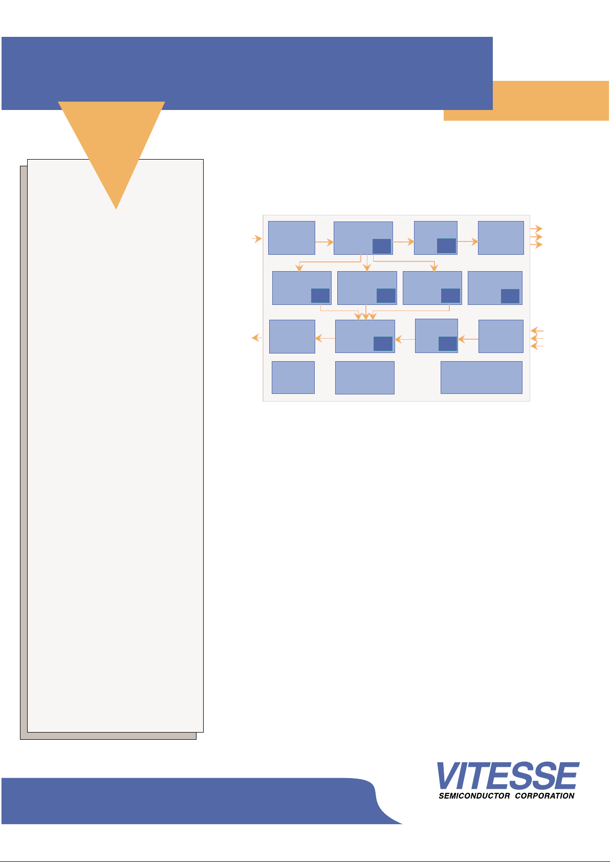
VSC9670 Block Diagram
1) A Clk/Data/Sync interface for
generic system connectivity , or
2) A 1.5/2/4/8 MHz interface to a
TDM backplane or standard timeslot-interchange, or
3) A V itesse open-architecture TDMe
interface connecting the VSC9670
to the VSC9680 HDLC/A TM
controllers.
TDMe Interface
TDMe Interface
Clock/Data/Sync
Clock/Data/Sync
Clock/Data
Clock/Data
TDM Bus
TDM Bus
RAM
RAM
RAM
RAM
RAM RAM
RAM
RAM
RX
Framer
SLIP Buffer
RX/TX
Facility
Data Link
RX/TX
Errors/
Counts
RX/TX
Robbed-bit
Signaling
TX
Framer
Intel/Motorola
CPU Interface
28 RX/TX
Jitter
Attenuators
Loop Back
Buffer
SLIP Buffer
TX Back End
(Serial
- to -
Parallel)
Scan
+
JTAG
TX Front End
(Parallel
- to -
Serial)
RX Front End
(Serial
- to -
Parallel)
RX Back End
(Parallel
- to -
Serial)
For more information on Vitesse Products visit the Vitesse web site
at www.vitesse.com or contact Vitesse Sales at (800) VITESSE or
sales@vitesse.com
© Copyright 2000 Vitesse Semiconductor Corporation
and the Vitesse logo
are all registered trademarks
of Vitesse Semiconductor Corp;oration
www.vitesse.com
Product Brief
TimeStream
Product
Family
28 T1 Framing Device
VSC9670
Transmit Section
System transmit data is converted to
an 8-bit wide data path, and a shared
state machine frames the data to
Superframe (SF) or Extended
Superframe (ESF) formats and calculates CRC-6 for ESF. Other shared
state machines perform alarm generation, facility data link handling, and
robbed-bit signaling. Data is then serialized and presented to the LIU or M13
multiplexer.
Receive Section
Each of the 28 received T1 bit streams
are converted to an 8-bit wide data
path, and a shared state machine performs framing, error and alarm detection, statistics, facility data link and
robbed-bit signaling functions. Slip buffers can be used to de-couple timing
between the line side and the system
side.
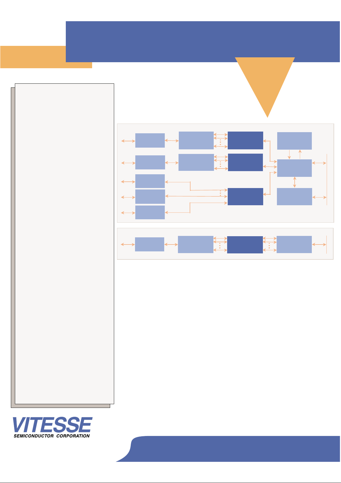
Application Diagrams
Features Continued:
• System-side signaling bus inter-
faces are available
• 2 separate indirect register banks
support ISR and User modes of
Driver operation
• IEEE 1 149.1 JTAG boundary scan
with T AP
• 456-pin EPBGA package; 3.3V
CMOS; 5V tolerant I/O
Applications:
• A TM & Frame Relay Switches
• Remote Access Concentrators
• SONET/SDH Add-Drop Mux
• Digital Access Cross Connects
• Routers with T1 interfaces
• Carrier-class IP Telephony
Switches
Standards:
• AT&T Publications TR-62411 -
Accunet T1.5 Service Description
and Interface Specification 12/90
• A T&T Publication TR-54106 - Re-
quirements for Interfacing Digital
Terminal Equipment to Services
Employing the Extended Super
Frame, 9/89
• AT&T Publication TR-43801 –
Channel Bank Requirements &
Objectives, 9/82
• ANSI T1.403-1995, Network-to-
customer Installation - DS1 Metallic Interface
• TR-303 Integrated Digital Loop
Carrier System Generic Requirements 1995
VSC9670
VSC9670
VSC9670
VSC9670
PACE
VSC9680 HLDC
M13
LIU
LIU
LIU
LIU
LIU
M13
SRAM
ATM SAR
TSI
(SC-4000
or equivalent)
LIU
M13
Channelized
T3 to TSI H.100
T3
T1
T1
T3
T3 plus multiple T1s for Frame Relay and ATM using VSC9670 and VSC9680
UTOPIA L2
T1
28 T1s
up to 28 T1s
28 T1s
PCI 32/64
33/66
MHZ
H.100
Channelized
Bus
28 Clk /Data/Sync
T3
45 MHZ
28 T1s
 Loading...