

VITESSE VSC880TY Datasheet
VITESSE
SEMICONDUCTOR CORPORATION
Data Sheet
VSC880
Features
• 16x16 Synchronous Serial Crosspoint Switch
• Serial Data Rates: 2.0Gb/s
• 32Gb/s Aggregate Data Bandwidth
• Parallel Switches Can Increase Data Bandwidth in
Multiples of 32Gb/s
• Designed in Conjunction with the VSC870
Backplane Transceiver
• Automatic Word and Cell Synchronization to the
Transceiver
• Two Modes of Operation: Distributed Control
Self-routing Packet Mode and Central Control
Cell Mode
• Multicast Supported in All Modes
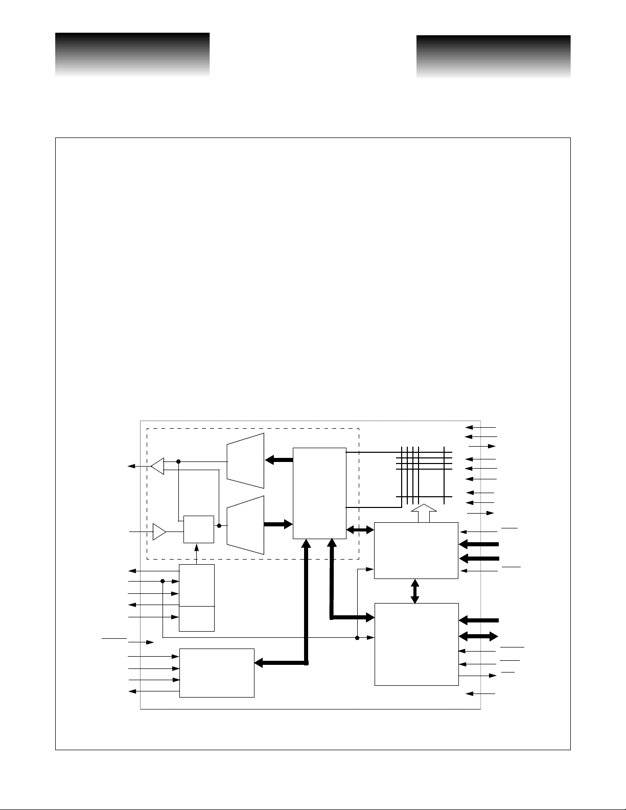
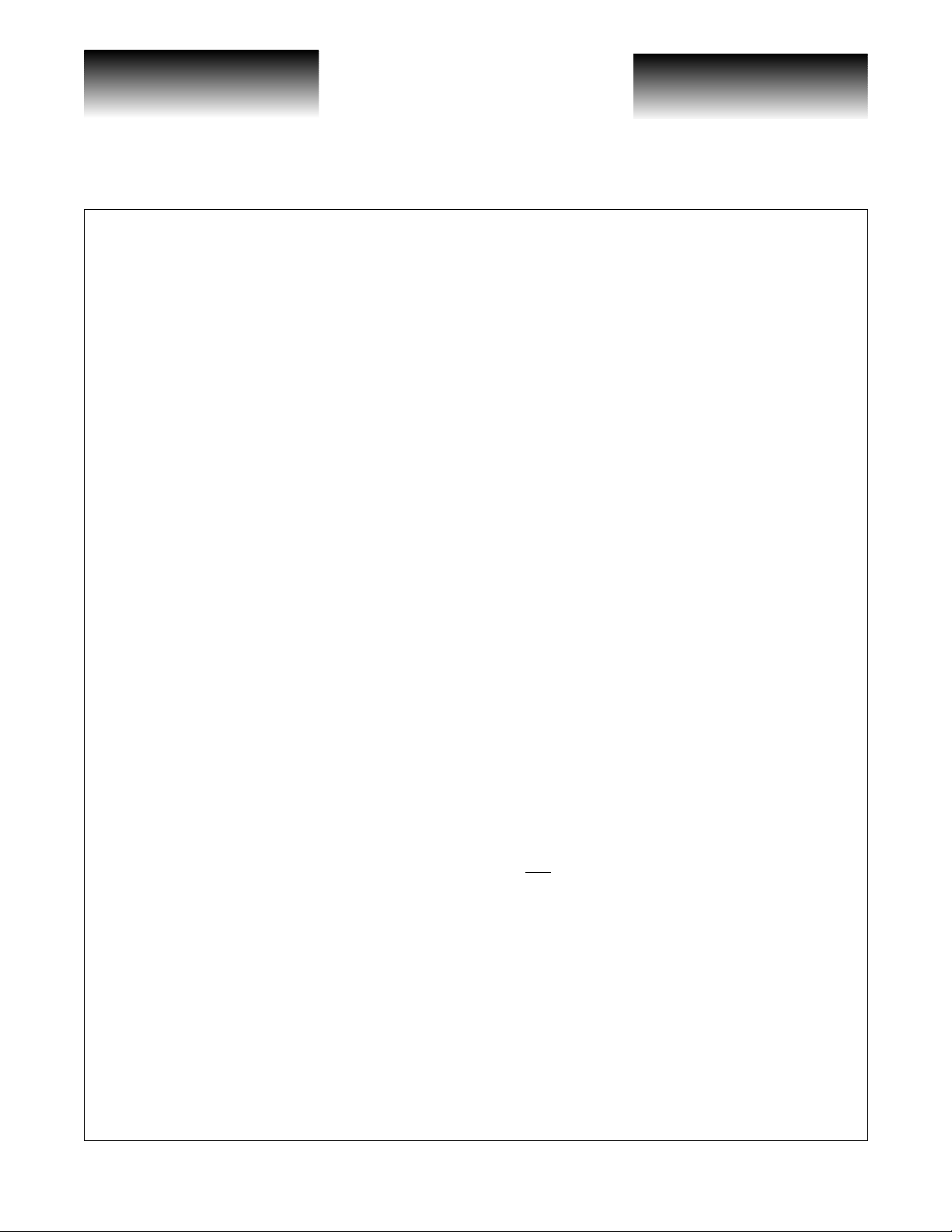
High Performance 16x16
Serial Crosspoint Switch
• Supports Variable Length Packets in Packet
Mode
• Built-in Flow Control Channel in Packet Mode
• Supports Cell Synchronization in Cell Mode
• Parallel CPU Interface and Parallel Switch
Configuration Interface
• Loopback, Built-in Self Test and Scan Functions
• 5V Tolerant TTL Inputs
• Dual 3.3V/2.5V or Dual 3.3V/2.0V Power
Supplies
• Serial Port Quadrants Can be Powered Down
• Available in 304 BGA Package
VSC880 Block Diagram
Serial Port (1 6x)
TXS+/TXS-
RXS+/RXS-
WCLK
REFCLK
TCLKEN
LOCKDET
CCLK
RESET
BSTLPBK
BSTEN
BSTRST
BSTPASS
DRU
CMU
Clock
Gen
BIST Logic
Parallel
to
Serial
Serial
to
Parallel
Port
Logic
Switch Matrix
Arbitration Logic
and Switch Control
Registers
Status and
Control Registers
VSCTE
VSCIPNC
VSCOPNC
MEN
FACLPBK
CMODE
TESTEN
SCANIN
SCANOUT
CEN
DATA[15:0]
FI[3:0]
WEN
ADDR[5:0]
CDATA[7:0]
CWEN
CSEL
INT
RESYNEN
G52191-0, Rev 4.2 Page 1
01/05/01
© VITESSE SEMICONDUCTOR CORPORATION • 741 Calle Plano • Camarillo, CA 93012
Tel: (800) VITESSE • FAX: (805) 987-5896 • Email: prodinfo@vitesse.com
Internet: www.vitesse.com
VITESSE
SEMICONDUCTOR CORPORATION
High Performance 16x16
Serial Crosspoint Switch
Data Sheet
VSC880
General Description
The VSC880 is a 16x16 serial crosspoint switch with serial data rates at 2.125Gb/s. The VSC880 has been
designed to operate with the VSC870 backplane transceiver to establish a synchronous high performance switching
system with an aggregate bandwidth of 32Gb/s. The switch chip transmits the master word clock (62.5Mb/s), and
master cell clock (if used) to all port cards through the serial data channels. The transceivers automatically perform
bit alignment, word alignment and cell alignment to the switch chip. The transceiver and switch chip have been
optimized for both self-routing and cell-based systems and include special commands for connection requests (selfrouting) and cell synchronous operation (cell based). In addition, a parallel CPU interface can be used to control
internal modes and read status information from the switch. A 20-bit interface can als o be used to pro gram the switch
matrix in 4 clock cycles. The switch chip runs of f of a 3.3V/2.5V or 3.3V/2.0V power supplies. The serial I/O buffers
contain on-chip termination resistors (see Application Note 34).
Pin Descriptions
Pin Name I/O
TXS[15:0]+/
TXS[15:0]-
RXS[15:0]+/
RXS[15:0]-
DATA[15:0] Configuration Data Input I
FI[3:0] Force IDLE Input I
CEN
WEN
ADDR[5:0] Data Address I
CSEL
CDATA[7:0] Status Data Output B
CWEN Control Write Enable I
Transmit Serial Outputs O
Receive Serial Inputs I
Configure Enable I
Wri te E nable I
Chip Select I
Freq
Type
2.125Gb/s
LVDS
2.125Gb/s
LVDS
62.5Mb/s
TTL
62.5Mb/s
TTL
62.5Mb/s
TTL
62.5Mb/s
TTL
62.5Mb/s
TTL
62.5Mb/s
TTL
62.5Mb/s
TTL
62.5Mb/s
TTL
Description
16 high speed serial di fferential transmit channels
16 high speed serial differential receive channels
Parallel input signals used to p rog ram t he switc h m atrix in 4
clock cycles when the signal CEN
Parallel input signals used to program force IDLE words at
the switch matrix output in 4 clock cycles when the signal
CEN
is LOW .
When CEN
can be used to program the switch matrix in 4 word clock
cycles timed to the WEN signal.
If CEN
for loading switch configuration data into DATA[15:0] and
FI[3:0].
The address to read and write data through parallel interface
CDATA[7:0].
This signal allows several switch chip s to sha re an 8 bi t d ata
bus connected to CDATA[7:0]. If CSEL
be read or written to CDATA[7:0]. If CSEL
outputs will be high impedance and the inputs disabled.
Bidirectional CPU interface for the status and control
registers. If CSEL
into this port. If CSEL
impedance and the inputs will be disabled.
This signal is set HIGH to read the internal status registers
through the parallel interface CDATA[7:0]. It is set LOW to
write into this interface.
is held LOW , the inputs DATA[15:0] and FI[3:0]
is LOW , this sign al provi des a syn chroniza tion pul se
is LOW, the data will be read or written
is HIGH, the outputs will be high
is LOW.
is LOW, data will
is HIGH, the
Page 2 G52191-0, Rev 4.2
© VITESSE SEMICONDUCTOR CORPORATION • 741 Ca l le Pl an o • Camarillo, CA 93012
Tel: (800) VITESSE • FAX: (805) 987-5896 • Email: prodinfo@vitesse.com
Internet: www.vitesse.com
01/05/01
VITESSE
SEMICONDUCTOR CORPORATION
Data Sheet
VSC880
Pin Name I/O
RESYNEN Resynch Enable I
INT
MEN Reserved I
FACLPBK Facility Loop Back I
CMODE Cell Mode I
TESTEN Scan Test Enable I
SCANIN Scan Data In I
SCANOUT Scan Data Out O
WCLK Word Clock O
REFCLK Reference Clock I
TCLKEN Test Clock Enable I
CCLK Cell Clock I
RESET
BSTLPBK
BSTEN Built-in Self Test Enable I
BSTRST Built-in Self Test Reset I
BSTPASS Built-in Self Test Pass O
Interrupt O
Reset I
Built-in Self Test Loop
Back
I
Freq
Type
<1MHz
TTL
<1MHz
TTL
<1MHz
TTL
<1MHz
TTL
<1MHz
TTL
<1MHz
TTL
62.5Mb/s
TTL
62.5Mb/s
TTL
62.5MHz
TTL
62.5MHz
TTL
<1MHz
TTL
62.5MHz
TTL
<1MHz
TTL
<1MHz
TTL
<1MHz
TTL
<1MHz
TTL
<1MHz
TTL
High Performance 16x16
Serial Crosspoint Switch
Description
If RESYNEN is HIGH, all links that have a link error
condition will be reinitia lized. This will o verride th e inter nal
control register settings.
is LOW, a receive error has occurred in one o f the
If INT
links that has it’s output enable (OE) bit set HIGH and
interrupt control register bit set HIGH.
This signal is reserved for future use and should be set LOW
during normal operation.
If this signal is set HIGH, all serial inputs are looped back to
their serial outputs. This will override the internal control
register setting.
CMODE is set HIGH for Cell Mode operation.
This signal is used in ATE testing to measure propagation
delay . It is a lso used i n AT E te sting o f the BIS T lo gic . S et to
logic LOW in normal operation.
The input signal for measuring propagation delay on the
ATE tester.
The output signal for measuring propagation delay on the
ATE tester. When TESTEN is set LOW, the longer delay
path is enabled.
This is the word clock output.
This is the reference clock and the source of the system wide
word clock period.
This input is set HIGH in test mode, so that the CMU is
bypassed and the REFCLK becomes the bit clock. This
signal is for ATE test only. Set LOW in normal operation.
This is the source of the system wide cell clock. It is
internally synchronized to the REFCLK. In Packet mode , set
this signal HIGH to enable external switch c onfigu ratio n for
BIST.
Global chip reset (active LOW)
When BSTLPBK is set HIGH and TESTEN is LOW, all
serial data output signals are looped back to their serial data
inputs. If BSTLPBK is set HIGH and TESTEN is HIGH,
only ports 0-7 are placed in lo opback.
When BSTEN is HIGH, at-speed built-in self testing is
enabled.
The BSTRST signal is set HIGH to reset the PRBS
generator and comparator.
The BSTPASS signal is HIGH if BTSEN is HIGH and the
PRBS comparator detects the correct pattern in built-in self
test mode.
G52191-0, Rev 4.2 Page 3
01/05/01
© VITESSE SEMICONDUCTOR CORPORATION • 741 Calle Plano • Camarillo, CA 93012
Tel: (800) VITESSE • FAX: (805) 987-5896 • Email: prodinfo@vitesse.com
Internet: www.vitesse.com
VITESSE
SEMICONDUCTOR CORPORATION
High Performance 16x16
Serial Crosspoint Switch
Pin Name I/O
LOCKDET CMU Lock Detect O
VSCTE NOR Chain Test Enable I
VSCIPNC NOR Chain Input I
VSCOPNC NOR Chain Output O
VDD1, VDD2,
VDD3, VDD4
VDDA CMU Power Supply P 3.3V Clean power supply for CMU
VSSA CMU Ground P 0V Clean ground for CMU
VMM Core Power Supply P 2 ~ 2.5V Core power supply
Serial Port Power
Supplies
Freq
Type
<1MHz
TTL
<1MHz
TTL
<1MHz
TTL
<1MHz
VECL
P3.3V
Data Sheet
VSC880
Description
This signal is LOW while the CMU is acquiring lock.
Used for ATE testing of the parametric NOR chain in the I/O
frame. Set to logic LOW during normal operation.
Used for ATE testing of the parametric NOR chain in the I/O
frame. Set to logic LOW during normal operation.
Used for ATE testing of the parametric NOR chain in the I/O
frame. Leave output open during normal operation.
VDD1 = Serial Port 0-3 power supply
VDD2 = Serial Port 4-7 power supply
VDD3 = Serial Port 8-11 power supply
VDD4 = Serial Port 12-15 power supply
Functional Description
The VSC880 switch can be used in conjunction with the VSC870 transceivers to support two modes of
operation: Packet Mode and Cell Mode. In Packet mod e, the ch ip s et pr ovides a sw itching sy stem to s upport v ariable
length, self-routing data packets. In Cell Mode, the chip set provides a cell synchronous switching system with a user
defined scheduler. In this mode, it can support only fixed length data packets (cells). Routing decisions are carried
out in the scheduler and crosspoint configuration is synchronized to a cell clock. The scheduler configures the switch
matrix using the parallel interface. To conserve power, each serial port quadrant can be powered down if not used.
The following section gives a detailed functional descrip tion of the operation of the switch chip. Most of the
discussion includes some of the transceiver operation (see the VSC870 data sheet). The two major operation modes
are described separately in the Packet Mode and the Cell Mode sections.
1.0 Common Features
1.1 Synchronization
1.1.1 Link Characteristic
The serial link is used to connect the switch chip to transceivers. These links operate at 2.125 Gb/s and are
initialized simultaneously at power up, or separately when a link error occurs. A link is first bit synchronized, then
word synchronized and, if CMODE is HIGH, cell synchronized. In Packet or Cell mode, the switch acts as the
master, generating the bit clock along with the word and cell boundary information. The transceivers act as slaves,
recovering the bit clock, word clock and cell clock. The transceiver also contains redundant serial inputs and outputs
which can be used with a redundant switch chip.
Page 4 G52191-0, Rev 4.2
© VITESSE SEMICONDUCTOR CORPORATION • 741 Ca l le Pl an o • Camarillo, CA 93012
Tel: (800) VITESSE • FAX: (805) 987-5896 • Email: prodinfo@vitesse.com
Internet: www.vitesse.com
01/05/01
VITESSE
SEMICONDUCTOR CORPORATION
Data Sheet
VSC880
High Performance 16x16
Serial Crosspoint Switch
1.1.2 Data Scrambling
To allow the VSC 870 CRU to recover the bit clock, a 15% edge transition density m ust be guaranteed on the
serial data links. All command words and connection request words contain this required density. In order to get this
density on data words, scrambling must be employed by the transceiver (see VSC870 data sheet).
1.1.3 Bit Synchronization
In Packet Mode and Cell Mode, th e switch acts as the sour ce of the bit clock. It multip lies the local 62.5MHz
reference clock by 34 to generate a 2.125GHz clock and uses this clock to serialize the 32-bit word and 2 overhead
bits. The transceiver receives and feeds this serial data stream to a digital CRU to recover the bit clock and
deserialize the data stream to a 32-bit word plus 2 overhead bits at 62.5MHz. The transceiver also uses this recovered
clock to serialize its transmit words th at are sent to the switch. In this way, the switch and all the transceivers are
frequency-locked to one clock source which is provided by the reference clock on the switch card. Because of this,
the switch chip needs to recover only the phase information on the serial receive channel using a data recovery unit
(DRU). The DRU is designed as a delay lock loop and remains phase-locked to the incoming data stream as long as
the temperature does not change by more than 20 °C after link initialization. If this temperature variation is exceeded,
a link error may occur causing the link to reinitialize. Because of this, system reset should be held until the system
reaches temperature stability before starting the link initializing process.
1.1.4 Word Synchronization
During power up or at reset, the transceiver can initiate the word synchronization process. First, the transceiver
sends reset patterns to the switch to request that the switch starts the initialization process. The switch, upon
receiving this request, will send out special ALIGN words. The transceiver receives this serial data stream and word
aligns to this ALIGN word by adjusting its own word boundary one bit at a time. Up on detecting the correct word
alignment, it starts the transmit word alignment process. In this process, the transceiver continuo usly sends ALIGN
words to the switch. The switch uses its own word clock (REFCLK) to detect this ALIGN word. If the transmitters
word is not aligned to the switch chip word clock when it arrives at the switch, the switch chip continues to send out
ALIGN words. After receiving 32 ALIGN words from the switch chip, the transceiver changes its transmit word
boundary by 1 bit position and repeats the p rocess (this limit s the distan ce from the transceiv er to the switch to less
than 180ns one way). If the switch detects the transceivers ALIGN word correctly, it sends IDLE words to the
transceiver to signal that the transmitter has now word synchronized with the switch. It also clears the internal
registers LERR, TERR, DERR and CERR and sets the signal INT
successfully initialized (see section 1.4).
HIGH if all the enabled serial channels are
1.1.5 Cell Synchronization
If CMODE is set HIGH, after the word synchronization process completes, the transceiver starts the cell
synchronization process. In this process, the transceiver detects the received cell clock (CCLK) sent from the switch
embedded in the alignment word. The switch delays the global cell clock to adjust out th e pipeline delay from the
transceiver to the switch. The switch ch ip does this by connecting each port to itself during link initialization. By
sending an ALIGN words to itself, the transceiver can adjus t the transmit clock until it is properly phase shifted
relative to the global cell clock. If cells are sent from the transceiver aligned to this transmit cell clock, they will
arrive at the switch aligned to the master cell clock which is originated at the switch. For this alignmen t process to
work, the minimum cell size is 8 words (32 bytes).
G52191-0, Rev 4.2 Page 5
01/05/01
© VITESSE SEMICONDUCTOR CORPORATION • 741 Calle Plano • Camarillo, CA 93012
Tel: (800) VITESSE • FAX: (805) 987-5896 • Email: prodinfo@vitesse.com
Internet: www.vitesse.com
VITESSE
SEMICONDUCTOR CORPORATION
High Performance 16x16
Serial Crosspoint Switch
Data Sheet
VSC880
1.1.6 Link Error Detection
There are four types of link errors that can be flagged on the receive serial links. Link errors are detected using
IDLE words. If a link error is detected, a bit in the LERR register is set HIGH for that particular channel (see section
1.4). After every 8 link errors, a bit in the TERR register is set HIGH. If the DRU goes out of range, a bit in the DERR
register is set HIGH. If the last word in the cell period is an IDLE word and it does not have b its B[1:0] set HIGH to
designate a cell clock, a bit in the CERR register will be set HIGH. If an error bit is set in any of these registers, the
signal can be programmed to go LOW and/or the link can be programmed to automatically start link
INT
initialization depending on the value loaded in to the I nterrupt Control R egister ( see section 1.4). These er ror reg ister
bits will be cleared if the link is reinitialized, or the registers are read. If the s ignal RESYNEN is set HIGH, link
initialization will begin immediately upon the detection of any of these errors. If the switch is used without IDLE
words, the user is responsible for detecting parity error conditions and restarting the link initialization process.
1.2 Data Encoding Format
To provide self-routing and cell synchronization, the transceiver and switch require special word formats.
Depending on the mode that the switch is u sed in, different word types are recognized by the switch. In both the
Packet and Cell Modes, the switch processes both data words and command words. They have the same format in
both modes and will be described in following section. The format for the connection request words and header
words are described later in the Packet Mode section.
1.2.1 Data Word Format on the Serial Data Lines
The data word format as seen at the serial output of the transceiver or switch chip is shown below. Two overh ead
bits are added by the transceiver or switch chip to designate a data word to the receiving switch chip or transceiver.
The serial data is transmitted with the MSB first.
33 32 31 30 29 28 27 26 25 24 23 22 21 20 19 18 17 16 15 14 13 12 11 10 09 08 07 06 05 04 03 02 01 00
B B
1 0
Where:
B[1:0]If Packet Mode, 01=Flow control channel,
D[31:0]32 bit data payload
D D D D
31 30 29 28
If Cell Mode, 01, 10, 11 = data
D D D D
27 26 25 24
10=Flow control channel ,
11=Acknowledge from switch chip or header word to switch chip
D D D D
23 22 21 20
D D D D
19 18 17 16
--------------- Da ta Payload ----------------
D D D D
15 14 13 12
D D D D
11 10 09 08
D D D D
07 06 05 04
D D D D
03 02 01 00
1.2.2 Command Word Format on the Serial Data Lines
The command word format as seen at the serial output of the transceiver or switch chip is shown below. Two
overhead bits are added by the trans ceiver or switch to designate a co mmand word (0 0) to the receiving switch chip or
transceiver. The serial data is transmitted with the MSB first. In Packet Mode, the IDLE word from the switch always
returns the current output connections for the port.
Page 6 G52191-0, Rev 4.2
© VITESSE SEMICONDUCTOR CORPORATION • 741 Ca l le Pl an o • Camarillo, CA 93012
Tel: (800) VITESSE • FAX: (805) 987-5896 • Email: prodinfo@vitesse.com
Internet: www.vitesse.com
01/05/01
VITESSE
SEMICONDUCTOR CORPORATION
Data Sheet
VSC880
33 32 31 30 29 28 27 26 25 24 23 22 21 20 19 18 17 16 15 14 13 12 11 10 09 08 07 06 05 04 03 02 01 00
0 0 1 B B
Where:
B[1:0]00=Undefined (during normal operation) or alignment word
01=Flow control channel,
10=Flow control channel,
11=Acknowledge (from switch chip only) or link initialization reset or cell clock in cell mode
C[4:0]Command type
D[15:0]Optional data payload
High Performance 16x16
Serial Crosspoint Switch
1 0
-- Command -- -- Data --
C C C C C
04 03 02 01 00
00XXX=Link Control (00000=ALIGN word, 00111=IDLE word)
01XX0=Command word for tr ansceiver (01000=set DLYEN/CCKIN value)
10XX0=Command word for switch
11XX0=Command word for receiving port card (TBD)
Default=1010101010101010
IDLE Word from switch=Current switch outputs this port is connected to
D[15] is for port 0, D[0] is for port 15
If C[4:0]=01000, D[3:0]=DLYEN/CCKIN value
D D D D
15 14 13 12
D D D D
11 10 09 08
D D D D
07 06 05 04
D D D D
03 02 01 00
1 0 1 0 1 0 1 0
1.2.3 IDLE Words
IDLE words are the default word used on t he ser ial channe l whe n none o f the other wo rd types are p resent. In
most cases, these words are automatically generated by the transceiver or switch chip. In Packet Mode, IDLE words
are inserted between pa ckets an d the ID LE wor d from th e switch always returns t he curre nt output c onnections for
the port that is receiving the ID LEs. Th ese connection bi ts will be in the s ame locat ion as in the C RQ word. In cell
mode, IDLEs will be transmitted from the s witch chip if the f orce IDLE (FI) bit i s set in the contro l registers. IDLE
words are also used to detect link error conditions. If the switch chip detects an IDLE word, it uses a bit mask to verify the proper bit pattern within the word.
1.3 Loopback
The VSC880 supports a loopback function at the serial interf aces which is used in built-in self -test mode. If th e
BSTLPBK signal is set HIGH and TESTEN is set LOW, the serial transmit data is looped back to the serial receive
side for all 16 channels. If the BSTLPB K signal is set HIGH and TESTEN is set HIGH, the serial transmit d ata is
looped back to the serial receive side for channels 0-7 only. If the FACLPBK signal is set HIGH, the serial receive
signal is looped back to the serial output for all 16 chann els. Each chan nel can also b e pro grammed to be loo ped b ack
separately from serial input to serial output b y using the control registers described below. The VSC880 does not
support simultaneous BIST and facilty loopback functions (either FACLPBK pin or LPBK[15:0] register).
1.4 Internal Register Definitions
The internal status and control registers are defined in the following table. The address signal ADDR[5:0] is used
along with CSEL
and HIGH to read from this port. If CSEL
and CWEN to read or write data through the CDATA[7:0] interface. CWEN is set LOW to write
is HIGH, the outputs become high impedance and the inputs become
G52191-0, Rev 4.2 Page 7
01/05/01
© VITESSE SEMICONDUCTOR CORPORATION • 741 Calle Plano • Camarillo, CA 93012
Tel: (800) VITESSE • FAX: (805) 987-5896 • Email: prodinfo@vitesse.com
Internet: www.vitesse.com
VITESSE
SEMICONDUCTOR CORPORATION
High Performance 16x16
Serial Crosspoint Switch
disabled. All data transfer timing is asynch ronous to REF CLK. The Interrupt Control Register is written by the user
to mask certain operations. If ICE is set HIGH, th e INT
register. If RCE is set HIGH, the link will automatically start link initiali zation if any error bit is set in the CERR
register. The corresponding pins can be used for the DERR, TERR and LERR registers. If the INT
the Interrupt Status Register can be read to determine which of the four registers received an error.
The CDEL[3:0] bits are used to program a value for the cell clock delay (see section 3.0). The switch matrix
status information can be read from the CN and FI registers. A serial link can be forced to reinitialize by writing a
HIGH into the RSY register. A serial output can be logically disabled by writing a HIGH into the OE register. A serial
input can be forced to loop back dir ectly to a serial ou tput b y wr iting a HI GH into th e LPBK re gister. All registers are
cleared upon RESET. Also, the LERR, TERR, DERR and CERR registers are cleared on reading.
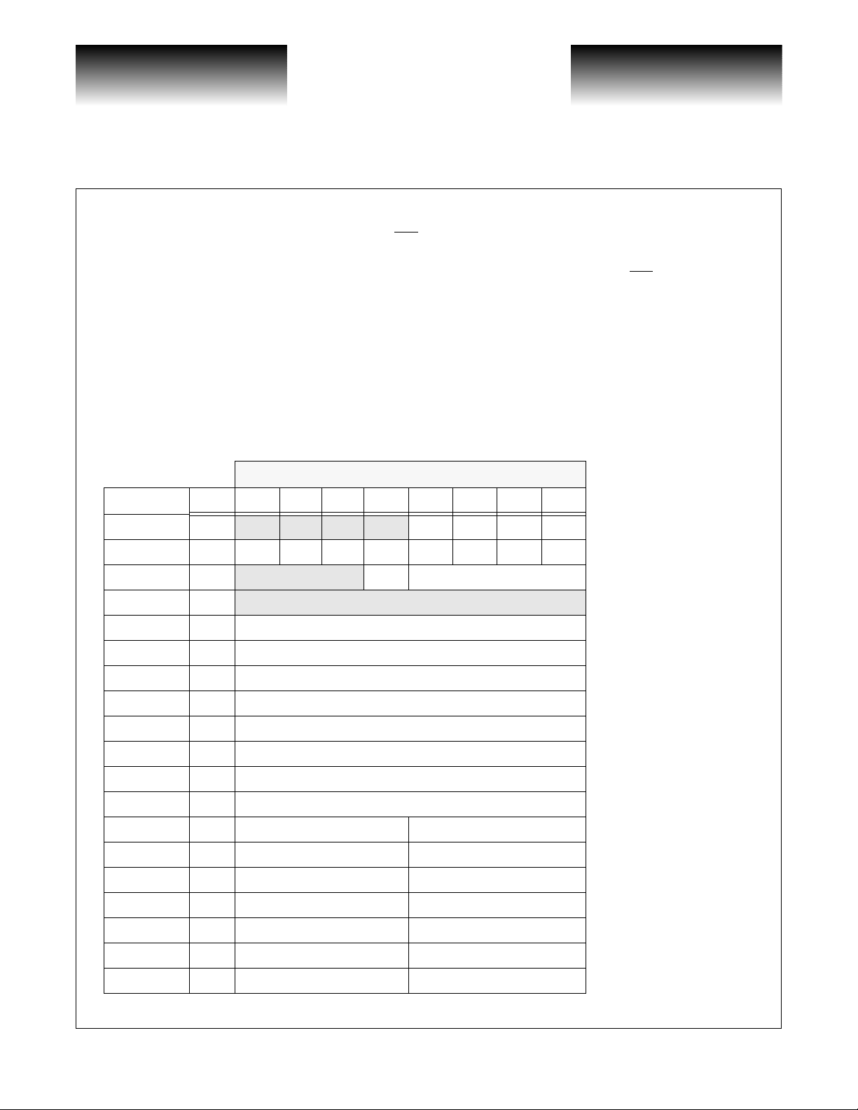
Figure 1: Status and Control Register Definition
CDATA[7:0] Bit Position
ADDR[5:0]R/W76543210
X 0 0 0 0 0 R CE DE TE LE Interrupt Status Register
output pin will go LOW i f any error bit is set in the C ERR
Data Sheet
VSC880
signal goes LOW,
X 0 0 0 0 1 R/W RCE RDE RTE RLE ICE IDE ITE ILE Interrupt Control Register
X 0 0 0 1 0 R/W BIST CDEL[3:0] BIST and Count Register
X 0 0 0 1 1
X 0 0 1 0 0 R CERR[7:0] CCLK error register LSB
X 0 0 1 0 1 R CERR[15:8] CCLK error register MSB
X 0 0 1 1 0 R DERR[7:0] DRU error register LSB
X 0 0 1 1 1 R DERR[15:8] DRU error register MSB
X 0 1 0 0 0 R TERR[7:0] Error threshold register LSB
X 0 1 0 0 1 R TERR[15:8] Error threshold register MSB
X 0 1 0 1 0 R LERR[7:0] Link error register LSB
X 0 1 0 1 1 R LERR[15:8] Link error register MSB
0 0 1 1 0 0 R/W C0[3:0] C8[3:0] Output0/Output8 Config
0 0 1 1 0 1 R/W C1[3:0] C9[3:0] Output1/Output9 Config
0 0 1 1 1 0 R/W C2[3:0] C10[3:0] Output2/Output10 Config
0 0 1 1 1 1 R/W C3[3:0] C11[3:0] Output3/Output11 Config
0 1 0 0 0 0 R/W C4[3:0] C12[3:0] Output4/Output12 Config
0 1 0 0 0 1 R/W C5[3:0] C13[3:0] Output5/Output13 Config
0 1 0 0 1 0 R/W C6[3:0] C14[3:0] Output6/Output14 Config
Page 8 G52191-0, Rev 4.2
© VITESSE SEMICONDUCTOR CORPORATION • 741 Ca l le Pl an o • Camarillo, CA 93012
Tel: (800) VITESSE • FAX: (805) 987-5896 • Email: prodinfo@vitesse.com
Internet: www.vitesse.com
01/05/01
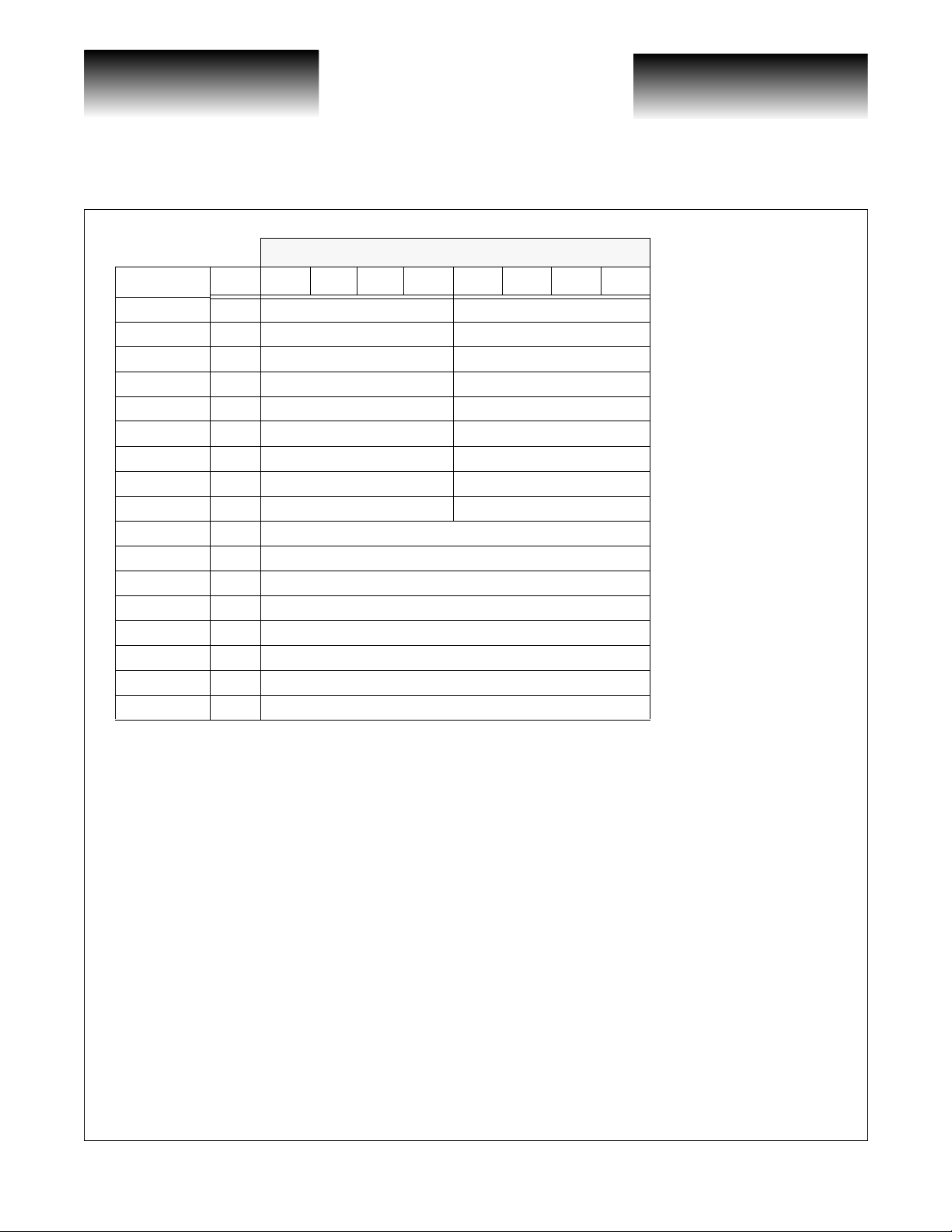
VITESSE
SEMICONDUCTOR CORPORATION
Data Sheet
VSC880
CDATA[7:0] Bit Position
ADDR[5:0]R/W76543210
0 1 0 0 1 1 R/W C7[3:0] C15[3:0] Output7/Output15 Config
1 0 1 1 0 0 R S0[3:0] S8[3:0] Output0/Output8 Status
1 0 1 1 0 1 R S1[3:0] S9[3:0] Output1/Output9 Status
1 0 1 1 1 0 R S2[3:0] S10[3:0] Output2/Output10 Status
1 0 1 1 1 1 R S3[3:0] S11[3:0] Output3/Output11 Status
1 1 0 0 0 0 R S4[3:0] S12[3:0] Output4/Output12 Status
1 1 0 0 0 1 R S5[3:0] S13[3:0] Output5/Output13 Status
1 1 0 0 1 0 R S6[3:0] S14[3:0] Output6/Output14 Status
1 1 0 0 1 1 R S7[3:0] S15[3:0] Output7/Output15 Status
X 1 0 1 0 0 R/W FI[7:0] Force IDLEs LSB
X 1 0 1 0 1 R/W FI[15:8] Force IDLEs MSB
X 1 0 1 1 0 R/W RSY[7:0] Resynch LSB
X 1 0 1 1 1 R/W RSY[15:8] Resynch MSB
X 1 1 0 0 0 R/W OE[7:0] Output Enable LSB
X 1 1 0 0 1 R/W OE[15:8] Output Enable MSB
X 1 1 0 1 0 R/W LPBK[7:0] Loopback LSB
X 1 1 0 1 1 R/W LPBK[15:8] Loopback MSB
High Performance 16x16
Serial Crosspoint Switch
Where:
CE Cell clock errorRCE Resynch on cell errorICE Interrupt on cell error
DE DRU error RDE Resynch on DRU errorIDE Interrupt on DRU error
TE Threshold errorRTE Resynch on thresh errorITE Interrupt on threshold error
LE Link error RLE Resynch on link errorILE Interrupt on link error
BIST Set this bit HIGH to test the BIST circuitry
CDEL[3:0] Cell clock delay
CERR[15:0]Cell clock error register, bit 0 is channel 0 etc, Cleared on read
DERR[15:0]DRU error register, bit 0 is channel 0 etc. Cleared on read
TERR[15:0]Threshold error register, bit 0 is channel 0 etc. Cleared on read
LERR[15:0]Link error register, bit 0 is channel 0 etc, Cleared on read
CN[3:0]Switch configuration data. N is the output port number, [3:0] is the input port connected. Default = 0xF.
SN[3:0]Output status data. N is the output port num ber, SN[3:2] = 00 for normal operation.
01 for out of synch
10 for word synch in progress
11 for cell synch in progress
SN[1] = Output busy in pac ke t mo de
SN[0] = Connection valid in packet mode
G52191-0, Rev 4.2 Page 9
01/05/01
© VITESSE SEMICONDUCTOR CORPORATION • 741 Calle Plano • Camarillo, CA 93012
Tel: (800) VITESSE • FAX: (805) 987-5896 • Email: prodinfo@vitesse.com
Internet: www.vitesse.com
 Loading...