

VITESSE
SEMICONDUCTOR CORPORATION
Data Sheet
VSC870
Features
• Performs 32-Bit Parallel to Serial and Serial to
Parallel Functions
• Serial Data Rates are 2.0Gb/s
• Designed in Conjunction with the VSC880 Serial
Crosspoint Switch
• Performs Bit Alignment, Word Alignment and
Cell Alignment
• Three Modes of Operation:
Distributed Control Packet Mode, Central
Control Cell Mode and Direct Mode
• Support for Multicast and Multiple Input Queues
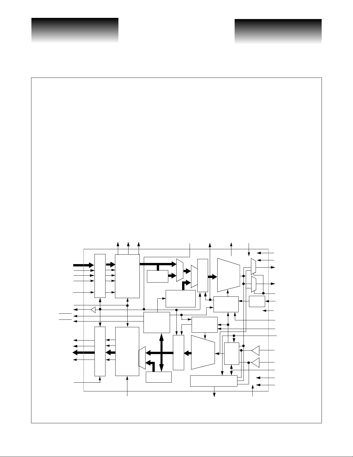
VSC870 Block Diagram
High Performance Serial
Backplane Transceiver
• Supports Priorities, Camp-on and
Retransmission Capability in Packet Mode
• Built-in Flow Control Channel in Packet Mode
• Supports Cell Synchronization in Cell Mode
• Interfaces Directly with Industry Standard
FIFOs
• Contains Redundant Serial I/Os and Internal
Loopback Mode
• 5V Tolerant TTL Inputs
• Single 3.3V Power Supply
• Available in 192 BGA Package
TXIN[31:0]
TXTYP[1:0]
TXEN
RTR
ABORT
BYPASS
WCLK
TXOK
RXOK
RXWA
RXTYP[1:0]
RXOUT[31:0]
ACK/RCLK
RXEN
RTM/TCLK
Register
Register
RFM
Transmit
Control
Receive
Control
CELLSYN
REN
SCRAM
Word/Cell
Aligner
DeSCRAM
WSIN
Alignment
Word Gen
Retiming
WSOUT
Retiming
TXCLK
Generator
RXCLK
Generator
Serial
to
Parallel
Signal Detect
ALIVE
OOS
Parallel
to
Serial
CRU
RESYNEN
CMU
LTIME
RESET
SCRAM
TXSA+/TXSA-
TXSB+/TXSB-
FACLPBK
REFCLK
DLYEN/CCKIN
MODE[1]
MODE[0]
LOOPBACK
RXSA+/RXSA-
RXSB+/RXSBRXSEL
TESTEN
VSCTE
G52190-0, Rev 4.1 Page 1
01/05/01
© VITESSE SEMICONDUCTOR CORPORATION • 741 Calle Plano • Camarillo, CA 93012
Tel: (800) VITESSE • FAX: (805) 987-5896 • Email: prodinfo@vitesse.com
Internet: www.vitesse.com

VITESSE
SEMICONDUCTOR CORPORATION
High Performance Serial
Backplane Transceiver
VSC870
General Description
The VSC870 serial backplane transceiver has been designed to op erate with the VSC880 se rial cro sspoint switch
to establish a synchronous high performance switching system. The VSC870 can also connect directly to another
transceiver to act as a high bandwidth backplane interconnect link. The transmitter converts a 32-bit parallel interface
operating at 62.5Mb/s to a 34-bit serial data stream operating a 2.125Gb/s. The receiver converts a 34-bit serial
interface operating at 2.125Gb/s to a 32-bit parallel interface operating at 62.5Mb/s. The transceiver performs
automatic bit alignment, word alignment and cell alignment to a connected switch chip or another transceiver. The
parallel interface has been designed with industry-standard FIFOs in mind to provide such features as automatic
packet retransmission, multicast with retransmission, camp-on and support for virtual output queues. These features
can also be bypassed to give the user direct control of the serial data stream. In addition, the transceiver and switch
chip can operate in a early arbitration mo de that greatly improves bandwidth utilization. The transceiver also contains
a built-in a flow control channel and redundant serial I/O buffers.
The transceiver and switch chip have been optimized to be used in both distributed-controlled packet-based
switching systems (Packet Mode), and centrally-controlled cell-based switching systems (Cell Mode). The
transceiver can also be directly connected to another transceiver (Direct Mode) for backplane interconnect
applications. The transceiver runs off a 3.3V power supply. The serial I/O buffers contain on-chip termination
resistors (See Figure 19).
Data Sheet
Page 2 G52190-0, Rev 4.1
© VITESSE SEMICONDUCTOR CORPORATION • 741 Ca l le Pl an o • Camarillo, CA 93012
Tel: (800) VITESSE • FAX: (805) 987-5896 • Email: prodinfo@vitesse.com
Internet: www.vitesse.com
01/05/01
VITESSE
SEMICONDUCTOR CORPORATION
Data Sheet
VSC870
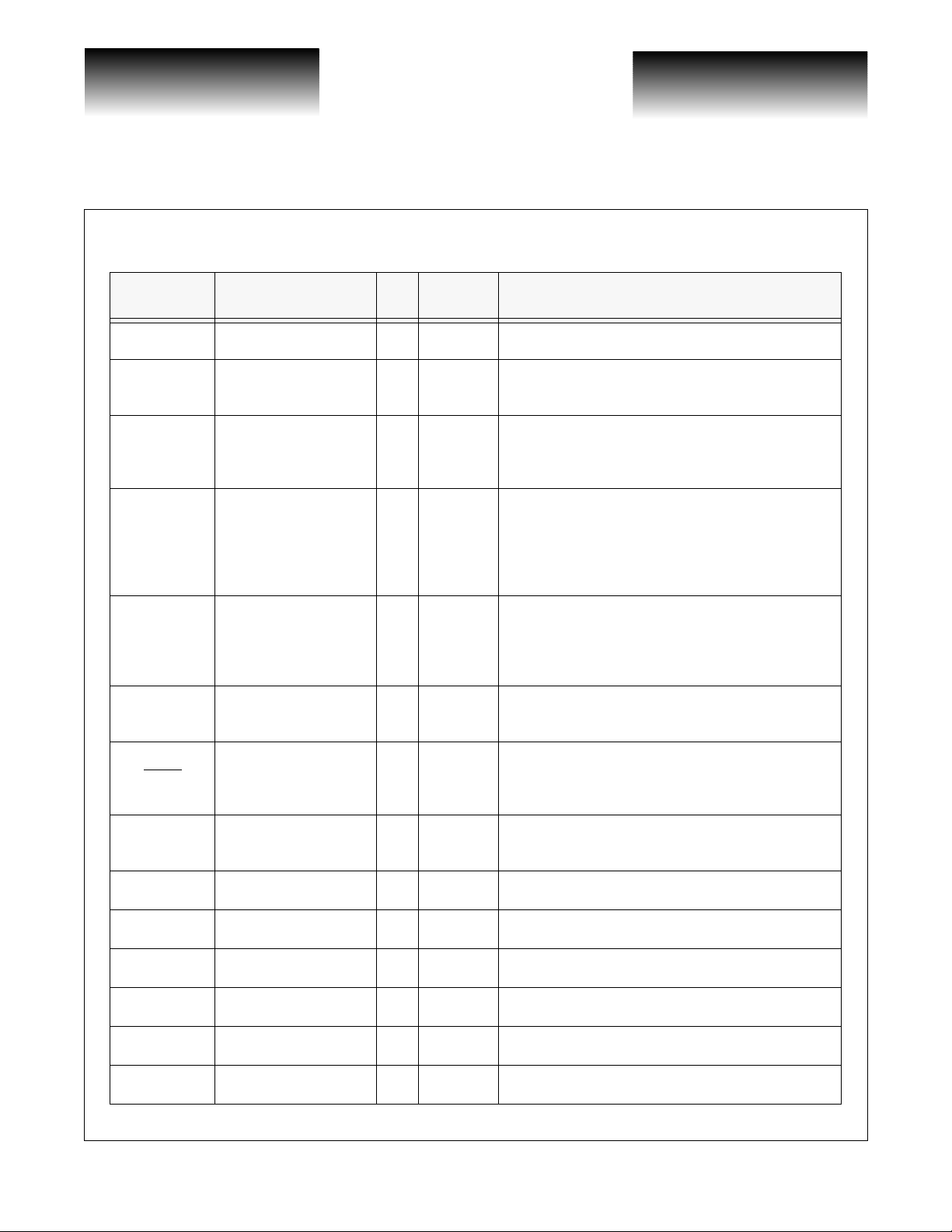
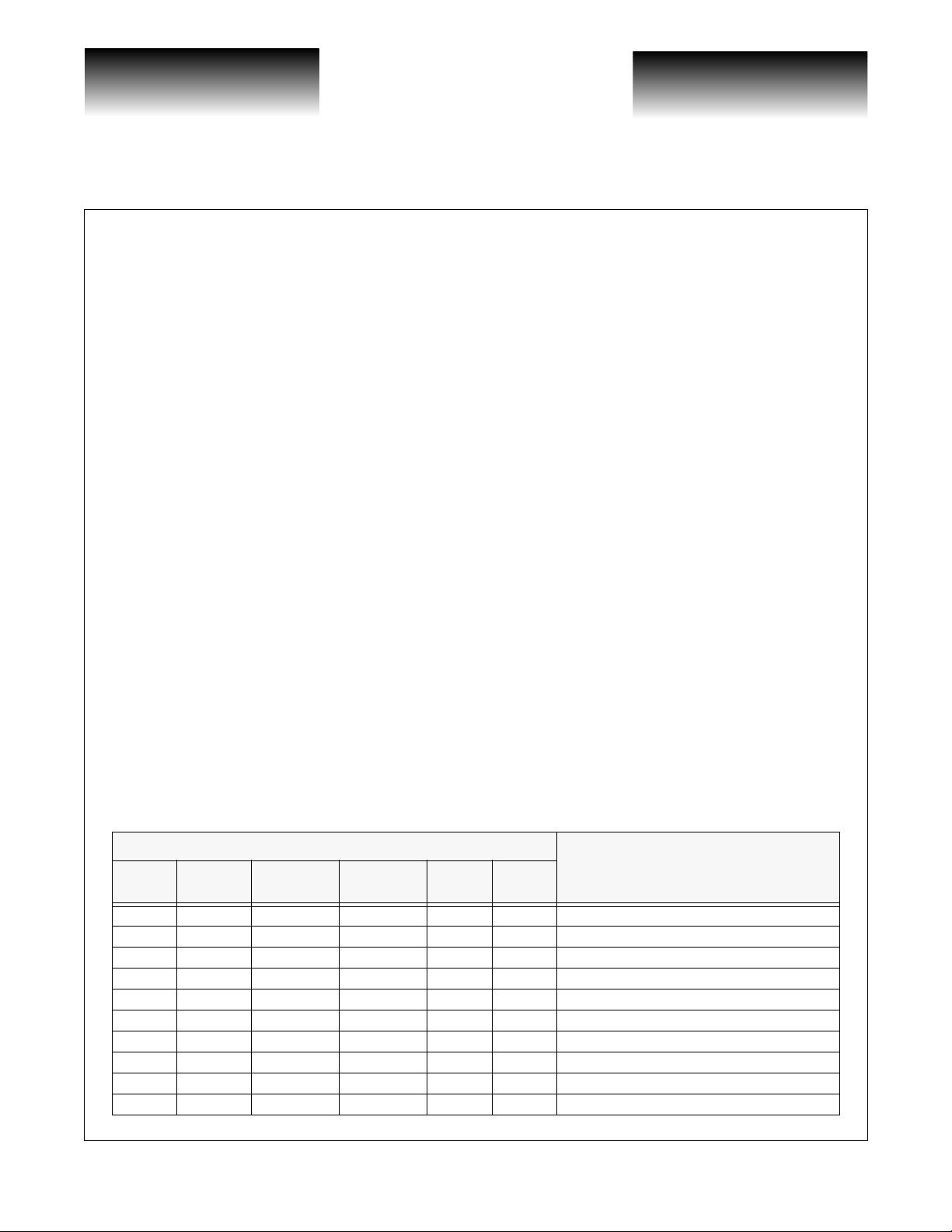
Package Pin Descriptions
Symbol Name I/O
TXIN[31:0] Transmit Parallel Data In I
TXTYP[1:0] Transmit Word Type I
TXEN Transmit Enable I
RTR Ready To Receive I
RTM/TCLK
RFM Read From Mark O
TXOK
REN Read Enable O
MODE[1:0] Mode Control I
TXSA+/
TXSA-
TXSB+/
TXSB-
LOOPBACK Loop Back I
RXSA+/
RXSA-
RXSB+/
RXSB-
Retransmit Mode/
Transmit Cell Clock
Transmit signal OK O
Transmit Serial Output A O
Transmit Serial Output B O
Receive Serial Input A I
Receive Serial Input B I
O
Freq
Type
62.5Mb/s
TTL
62.5Mb/s
TTL
62.5Mb/s
TTL
62.5Mb/s
TTL
62.5Mb/s
TTL
62.5Mb/s
TTL
<1MHz
TTL
62.5Mb/s
TTL
<1MHz
TTL
2.125Gb/s
LVDS
2.125Gb/s
LVDS
<1MHz
TTL
2.125Gb/s
LVDS
2.125Gb/s
LVDS
High Performance Serial
Backplane Transceiver
Description
32-bit parallel data input for the transmit side.
If BYPASS is LOW, these signals designate the transmit
word type. If BYPASS is HIGH, these signals directly
control the overhead bits sent on the serial channel.
When TXEN is HIGH, TXIN[31:0], TXTYP[1:0] are
loaded in to the transcei ver on the next WCLK. When
TXEN is LOW, the transceiver ignores TXIN[31:0] and
TXTYP[1:0] and sends IDLE words at the serial output.
When RTR is HIGH, the receiving sid e memory system is
ready to receive dat a. If LOW, it sends a back pressure
(flow control) signal to the source port card telling it to
stop sending data. In Cell Mode, set RTR LOW to cell
synchronize to the external ce ll cl ock. If RTR is HIGH,
cell clock is recovered from the bit stream.
In Packet Mode, when BYPASS is LOW, RTM/TCLK is
set HIGH at the beginning of each data tr ansmission and
set LOW when the data packet has been successfully sent
to all outputs. In Cell Mode, a HIGH pulse represents the
transmit cell clock.
When BYPASS is LOW, RFM is set HIGH whenever a
retransmission of data is required due to contention for
destination ports.
This signal is LOW if MODE[1] is HIGH and the
transceiver is word aligned on the transmit side. After
initialization it will go HIGH for one word clock if there
is a cell clock error.
When REN is HIGH, the transceiver is ready to read data
at TXIN[31:0] and TXTYP[1:0]. This signal can be
forced low by the received flow control signal.
These mode control pins are used to configure link
synchronization . S ee Section 1.5.
High speed serial differential tran smit channel A
High speed serial differential tran smit channel B
When LOOPBACK is HIGH, the CRU and signal
detector select the serial data output channel as an input.
High speed serial differential receive ch annel A
High speed serial differential receive ch annel B
G52190-0, Rev 4.1 Page 3
01/05/01
© VITESSE SEMICONDUCTOR CORPORATION • 741 Calle Plano • Camarillo, CA 93012
Tel: (800) VITESSE • FAX: (805) 987-5896 • Email: prodinfo@vitesse.com
Internet: www.vitesse.com
VITESSE
SEMICONDUCTOR CORPORATION
High Performance Serial
Backplane Transceiver
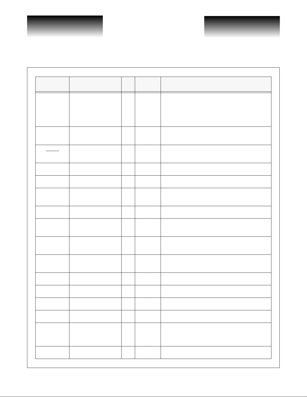
Symbol Name I/O
RXSEL Receive Input Select I
ALIVE Redundant Input Alive O
RXOK
RXEN Receive Enable I
RXOUT[31:0]
RXTYP[1:0] Receive Word Type O
RXWA Receive Word Available O
ACK/RCLK
ABORT
WSIN Word Synch In I
WSOUT Word Synch Out O
RESYNEN Resync Enable I
OOS Out Of Sync O
SCRAM S cr a m ble Enable I
BYPASS Bypass Mode I
CELLSYN
Receive Signal OK O
Receive Parallel Data
Out
Acknowledge /
Receive Cell Clock
Connection Request
Abort
Cell Synchronization
Enable
O
O
I
I
Freq
Type
<1MHz
TTL
<1MHz
TTL
<1MHz
TTL
62.5Mb/s
TTL
62.5Mb/s
TTL
62.5Mb/s
TTL
62.5Mb/s
TTL
62.5Mb/s
TTL
62.5Mb/s
TTL
62.5MHz
TTL
62.5MHz
TTL
<1MHz
TTL
<1MHz
TTL
<1MHz
TTL
<1MHz
TTL
<1MHz
TTL
Data Sheet
VSC870
Description
When RXSEL is LOW and LOOPBACK is LOW, RXSA
is selected as the input to the CRU and RXSB is selected
as the input to the Signal Detector. When RXSEL is
HIGH and LOOPBACK is LOW, RXSB is selected as the
input to the CRU and RXSA is selected as the inpu t to the
Signal Detector.
This output is high if at least one edge transition is
detected every word clock period on the redundant input
serial lin e.
This signal goes LOW if the VSC870 is word aligned on
the receive side. After initialization, it goe s HIGH if there
is error in the IDLE words.
When RXEN is LOW, the RXOUT[31:0] and
RXTYP[1:0] outputs become high impedance.
32-bit parallel data output for the receive side.
If BYPASS is LOW, these signals tell the received word
type. If BYPASS is HIGH, these signals reflect the
overhead bits received on th e serial channel.
When RXWA is LOW, RXTYP[1:0] and RXOUT[31:0]
is an IDLE word.
In Packet Mode, t he ACK signal will be set high if a
Connection Request on the transmit side is granted. In
Cell mode, a high pulse represents the receive cell cloc k.
When BYPASS is LOW and ABORT is HIGH, the
connection request and data transmission process is
aborted.
The WSIN sign al provides the word clock input and mus t
be driven by a signal frequency locked to the WSOUT
signal either from itself or another transceiver.
The WSOUT signal is the internally generated word clock
and is synchronized to the transmit word clock.
If RESYNEN is HIGH and the transceiver detects a link
error, it will start the Link Initialization process.
If OOS is HIGH, the transceiver is in the link
initialization process. It is LOW during normal operation.
If SCRAM is HIGH, data words will be scrambled and
descrambled.
BYP ASS is set HIGH for direct control and monitoring of
the overhead bits in the serial data strea ms as in cel l mode
and direct mode. This also disables the transceiver Packet
Mode functions.
CELLSYN is set HIGH to allow cell synchronization
during link initialization.
Page 4 G52190-0, Rev 4.1
© VITESSE SEMICONDUCTOR CORPORATION • 741 Ca l le Pl an o • Camarillo, CA 93012
Tel: (800) VITESSE • FAX: (805) 987-5896 • Email: prodinfo@vitesse.com
Internet: www.vitesse.com
01/05/01
VITESSE
SEMICONDUCTOR CORPORATION
Data Sheet
VSC870
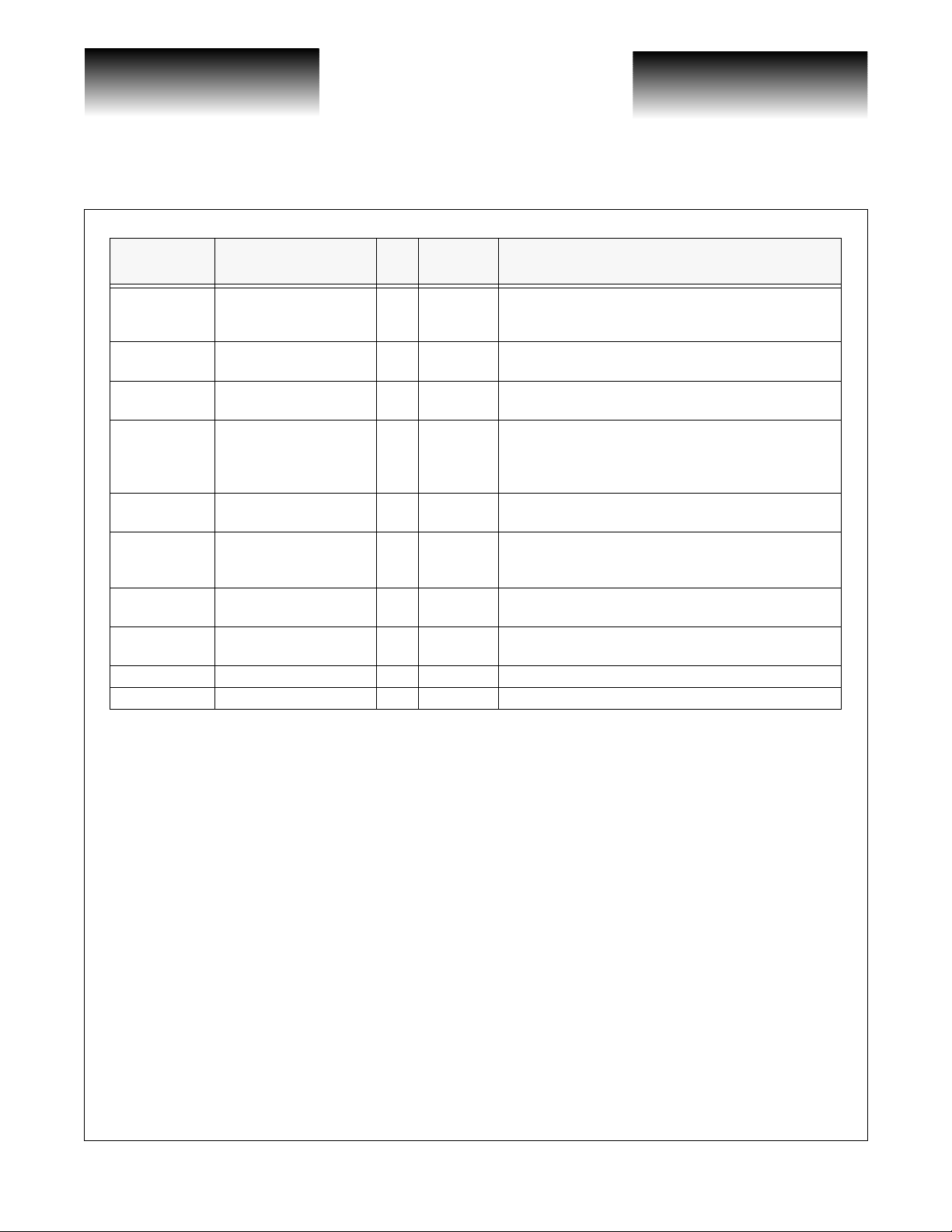
Symbol Name I/O
DLYEN/
CCKIN
FACLPBK Facility Loopback I
WCLK Word Clock O
REFCLK Local Reference Clock I
RESET Reset I
TESTEN Scan Test Enable I
LTIME Loop Time Mode I
VSCTE NOR Chain Test Enable I
VDDA CMU Power Supply P 3.3V Clean power supply for CMU
VSSA CMU Ground P 0V C lean ground for CMU
Delay Enable/Cell Clock
Input
I
Freq
Type
<1MHz
TTL
<1MHz
TTL
62.5MHz
TTL
62.5MHz
TTL
<1MHz
TTL
<1MHz
TTL
62.5Mb/s
TTL
<1MHz
TTL
High Performance Serial
Backplane Transceiver
Description
If BYP ASS is LOW, this signal can be set HIGH to enable
REN delay mode. In Cell Mode, DLYEN/CCKIN can be
used as an input for cell clock alignment.
When this signal is HIGH, the serial input is looped back
to the serial output. It should be normally set LOW.
The word clock is a delayed version of the WSIN signal .
A 62.5 MHz local reference clock that is used to keep the
CRU close to the incoming bit clock frequency before the
alignment process begins. Is also used as a reference
clock for the CMU.
Global chip reset (active HIGH).
When TESTEN is HIGH, the REFCLK is used in place
of the bit clock for low speed testing. Used for ATE
testing only. Set to logic LOW during normal operation.
LTIME is set HIGH to use the recovered bit clock for the
transmit side.
Used for ATE testing of the parametric NOR chain in the
I/O frame. Set to logic LOW during normal operation.
G52190-0, Rev 4.1 Page 5
01/05/01
© VITESSE SEMICONDUCTOR CORPORATION • 741 Calle Plano • Camarillo, CA 93012
Tel: (800) VITESSE • FAX: (805) 987-5896 • Email: prodinfo@vitesse.com
Internet: www.vitesse.com

VITESSE
SEMICONDUCTOR CORPORATION
High Performance Serial
Backplane Transceiver
VSC870
Functional Description
Data Sheet
The VSC870 transceiver can be used in one of the three operation modes: Packet Mode, Cell Mode and Direct
Mode. In Packet mode, the VSC870 is intended to work in conjunction with the VSC880 switch chip to provide a self
routing switching system and to support variable length data packets. In Cell Mode, the transceiver works in
conjunction with the VSC880 switch chip to provide a cell synchronized switching system. In this mode, it can
support only fixed length data packets (cells), and routing decisions are carried out in a user defined controller chip
and synchronized to a cell clock. In Direct mode, the VSC870 can connect to other transceivers to provide a high
bandwidth serial backplane data link.
The following sections give a detailed description of generic features which are provided in all three modes,
followed by the operation of the transceiver in each mode. Most of the discussions in this data sheet include some of
the switch chip functions (see the VSC880 data sheet).
1.0 Common Features
1.1 Synchronization
1.1.1 Link Characteristic
The serial link is used to connect the transceivers to the switch chip or to other transceivers. These links operate
at 2.125Gb/s and are initialized simultaneously at power up, or separ ately when a li nk error occurs. A l ink is first bit
synchronized, then word synchronized and, if CELLSYN is HIGH, cell synchronized. In Packet or Cell mode, the
switch acts as the master, generating the bit clock along with the word and cell boundary information. The
transceivers act as slaves, recovering the bit clock, word clock and cell clock. In Direct mode, the transceivers can be
configured as either masters or slaves using the MODE[1:0] signals, with the masters generating the bit and word
clocks. The transceiver also contains redundant serial inputs and outputs which can be used with a redundant switch
chip or redundant transceiver.
1.1.2 Data Scrambling
A 15% edge transition density must be guaranteed on the serial data links for the CRU to work properly. All
command words and connection request words contain this required density. In order to get this density on data
words, scrambling is employed. If SCRAM is set HIGH, the 32-bit data words are scrambled in the transmitter and
de-scrambled in the receiver with a (1+X
used in SONET scrambling. In all operating modes, data words are recognized by TXTYP[1:0] = 01 or 10. Words
such as the connection request and header word in Packet Mode or cell clock in Cell Mode or the IDLE word in
Direct Mode are used to initiate the scrambling pattern. If the user can guarantee edge densities greater than or equal
to 15%, scrambling can be turned off by setting SCRAM = LOW.
1.1.3 Bit Synchronization
In Packet and Cell Mode, the switch acts as the source of the bit clock. It multiplies the local 62.5MHz word
clock by 34 to generate a 2.125GHz clock, and uses this clock to serialize the 32-bit data word and 2 overhead bits.
1+X7
) pattern to guarantee high transition density. This is the same pattern
Page 6 G52190-0, Rev 4.1
© VITESSE SEMICONDUCTOR CORPORATION • 741 Ca l le Pl an o • Camarillo, CA 93012
Tel: (800) VITESSE • FAX: (805) 987-5896 • Email: prodinfo@vitesse.com
Internet: www.vitesse.com
01/05/01
VITESSE
SEMICONDUCTOR CORPORATION
Data Sheet
VSC870
The transceiver receives and feeds this serial data stream to a digital CRU to recover the bit clock and deserialize the
data stream to a 32 bit word plus 2 overhead bits at 62.5MHz. The transceiver also uses this recovered clock to
serialize its transmit data words that are sent to the switch. In this way, the switch and all the transceivers are
frequency-locked to one clock source which is provided by the word clock on the switch card. The transceiver
provides its own CMU which multiplies a local REFCLK by 34. The output of the CMU helps the CRU obtain lock
and provides the clock source for the transceiver in loopback mode. This local REFCLK must be within 100ppm of
the switch chip reference clock frequency. In Direct Mode, the master transceiver uses the CMU to provide a clock
for the transmit data. The slave receivers recover the clock from the serial bit streams.
High Performance Serial
Backplane Transceiver
1.1.4 Word Synchronization
During power up or at reset, the transceiver can initiate the word synchronization process. First, the transceiver
sends reset patterns to the switch (or th e master transceiver in Direct mode) to request that the switch starts the
initialization process. The switch, upon receiving this request, will send out special ALIGN words. The transceiver
receives this serial data stream from the switch, and uses the RXCLK Generator to adjust the receive word clock
boundary one bit at a time until the Word/Cell Aligner detects proper alignment. Upon detecti ng the correct word
alignment, the RXOK
process, the transceiver continuously sends ALIGN words to the switch using the Alignment Word Generator. The
switch uses its own word clock to detect this ALIGN word. If the transmitters word is not aligned to the switch chip
word clock when it arrives at the switch, the switch chip continues to send out ALIGN words. After receiving every
32 ALIGN words from the switch chip, the transceiver changes its transm it word boun dary by one bit p osition usi ng
the TXCLK Generator and then repeats the process (this limits the distance from the transceiver to the switch to less
then 180nS one way). If the switch detects this ALIGN word correctly, it sends IDLE words to the transceiver to
signal that the transmitter has now word synchronized with the switch. When the transceiver detects these IDLE
words, the signal TXOK
RXTYP[1:0] are then phase aligned to the word clock (WSOUT).
The transmit word clock is output on the pin WSOUT. If a single transceiver is used on a port card, WSOUT
must be tied directly to WSIN. The signal WSIN is the clock input for all of the transceiver parallel logic and
provides the word clock output (WCLK). Retiming blocks are used in the transceiver to span the phase boundary
between WSIN and the transmit word clock and the receive word clock. If two or more transceivers are used in
parallel on a port card in order to increase bandwidth, each will have i ts own transmit word clock. Since these word
clocks are derived from the same source on the switch card, they will have the same frequency but a phase difference
of up to 8nS. This phase difference (skew) depends on the I/O delay of the switch and transceiver and the serial data
line delay between these chips. To properly phase align all transceiver parallel interfaces, one transceiver acts as the
master, providing its WSOUT signal not only to its own WSIN, but the WSIN on all other transceivers on the port
card (see Application Note 32: Design Guide for a Cell Based Switch with Central Control). This means that the
parallel logic blocks on all transceivers are clocked by the same source derived from the transmit word clock of the
master transceiver. In this way, skew between the parallel interfaces on all transceivers is minimized. Other logic on
the port card can be clocked using WSOUT of the master transceiver, or the WCLK output of any transceiver which
is a delayed version of WSOUT. A phase shifted word clock can also be used to drive WSIN provided that it is
frequency locked to the WSOUT signal. In this way, both the receive and transmit parallel interfaces can be phase
aligned to this word clock.
signal is set LOW and the word alignment process is started on the transmit side. In this
goes LOW and the parallel data signals TXIN[31:0], TXTYP[1:0], RXOUT[31:0] and
G52190-0, Rev 4.1 Page 7
01/05/01
© VITESSE SEMICONDUCTOR CORPORATION • 741 Calle Plano • Camarillo, CA 93012
Tel: (800) VITESSE • FAX: (805) 987-5896 • Email: prodinfo@vitesse.com
Internet: www.vitesse.com
VITESSE
SEMICONDUCTOR CORPORATION
High Performance Serial
Data Sheet
Backplane Transceiver
1.1.5 Cell Synchronization
If the CELLSYN signal is set HIGH, after the word synchronization process, the transceiver starts the cell
synchronization process. In this process, the transceiver detects the received cell clock sent from the switch. The cell
clock is embedded in the command words with overhead bits ‘00’ as described in section 3.2. The received cell clock
is output on ACK/RCLK. The switch chip connects each port to itself after link initialization. By sending a special
ALIGN word to itself, the transceiver can adjust the transmit cell clock (RTM/TCLK) until it is properly phase
shifted relative to the received cell clock. If cells are sent from the transceiver aligned to this transmit cell clock, they
will arrive at the switch aligned to the master cell clock which is originated at the switch. The received cell clock on
the serial link is therefore shifted by N word clocks to create a phase shifted cell clock which is output on RTM/
TCLK. An on-chip counter provides this phase shift, with the frequency and phase shift determined during the cell
synchronization process. For this alignment process to work, the minimum cell size is 13 words (52 bytes).
1.1.6 Cell Synchronization for Multiple Transceivers
If two or more transceivers are used in parallel on a port card in order to increase bandwidth, skew between
signals could cause the transmit cell clock (RTM/TCLK) in one or more transceivers to be shifted in phase b y one
word clock relative to the other transceivers. To adjust out this offset, a marker cell clock can be sent to both
transceivers. This is done by send ing the signal RTM/TCLK f rom the mas ter tran sceiver to the DL YEN/CCKIN in put
on the slave transceivers. At the end of the cell synchronization process, the pipeline offset is adjusted out using this
marker cell clock. See Application Note 32 for more details.
VSC870
1.1.7 Link Error Detection
Receive errors are declared if the transceiver detects a bit pattern error in an IDLE word in the received serial
data by generating a HIGH pulse on RXOK. In cell mode, if an IDLE word is received at the end of the cell period
and it does not contain the embedded cell clock, or it receives an embedded cell clock at the wrong time, it generates
a HIGH pulse on TXOK
link initialization process. The RXOK and TXOK signals can therefore be tied to th e RESYNEN signal to start the
link initialization process immediately, or the user logic can monitor the RXOK
LOW and assert RESYNEN only after an error threshold has been reached. It is up to the user to make sure enough
IDLE words are used to detect errors during system operation. The sw itch can initiate the initialization process by
forcing zeroes on the serial link. If the transceiver receives 4 cons ecutiv e word s of all zer oes , it will immediately s tart
the initialization process.
. This error is stored internally and if the RESYNEN goes HIGH, the VSC870 will start the
and TXOK signals when OOS is
1.2 Data Encoding Format
To provide self routing and signalling functions, the transceiver and switch require different data types to
differentiate between data words, connection request words or command words. Depending on the mode that the
transceiver is in, different data types are recognized at the transceiver parallel interface. These word types are
encoded using the RXTYP[1:0] or TXTYP[1:0] bits. At the transceiver to switch serial interface, these data types are
encoded in the two overhead bits (B[1:0]). Sections 2.2, 3.2 and 4.2 describe these data types in more detail.
The format for data words and command words the transceiver parallel interfaces and on the serial data lines
between the transceiver and switch chip are described in the following sections. The format for the connection
request word is described later in the Packet Mode section.
Page 8 G52190-0, Rev 4.1
© VITESSE SEMICONDUCTOR CORPORATION • 741 Ca l le Pl an o • Camarillo, CA 93012
Tel: (800) VITESSE • FAX: (805) 987-5896 • Email: prodinfo@vitesse.com
Internet: www.vitesse.com
01/05/01
VITESSE
SEMICONDUCTOR CORPORATION
Data Sheet
VSC870
High Performance Serial
Backplane Transceiver
1.2.1 Data Word Format at Transceiver Parallel Interface
Data words contain a 32 bit user defined payload which is sent between the transmitting and receiving port cards
as shown below. The RXTYP[1:0] and TXTYP[1:0] data word encoding format for different modes are described in
later sections.
31 30 29 28 27 26 25 24 23 22 21 20 19 18 17 16 15 14 13 12 11 10 09 08 07 06 05 04 03 02 01 00
D D D D
31 30 29 28
Where:
D[31:0]32 bit data payload
D D D D
27 26 25 24
D D D D
23 22 21 20
D D D D
19 18 17 16
--------------- Da ta Payload ----------------
D D D D
15 14 13 12
D D D D
11 10 09 08
D D D D
07 06 05 04
D D D D
03 02 01 00
1.2.2 Data Word Format on the Serial Data Lines
The data word format as seen at the serial output of the transceiver or switch chip is shown below. Two overhead
bits are added by the transceiver or switch chip to designate a data word to the receiving switch chip or transceiver.
The serial data is transmitted with the MSB first (B1, B0, D31, D30... D00).
33 32 31 30 29 28 27 26 25 24 23 22 21 20 19 18 17 16 15 14 13 12 11 10 09 08 07 06 05 04 03 02 01 00
B B
1 0
D D D D
31 30 29 28
D D D D
27 26 25 24
D D D D
23 22 21 20
D D D D
19 18 17 16
--------------- Da ta Payload ----------------
D D D D
15 14 13 12
D D D D
11 10 09 08
D D D D
07 06 05 04
D D D D
03 02 01 00
Where:
B[1:0]If BYPASS=0,01=Flow control channel,
10=Flow control channel,
11=Acknowledge from switch chip or data header to switch chip
If BYPASS = 1, RXTYP[1:0]=B [1:0 ]=TXT YP[1:0 ]
D[31:0]32 bit data payload
1.2.3 Command Word Format at Transceiver Parallel Interface
There are several command words that are used for sending information to the switch chip or a receiving port
card. The command word format at the transceiver parallel interface is shown b elow. IDLE words are discussed in the
next sections. A delay enable value can also be programmed into the transceiver for Packet Mode using this
command word.
31 30 29 28 27 26 25 24 23 22 21 20 19 18 17 16 15 14 13 12 11 10 09 08 07 06 05 04 03 02 01 00
X X X C C C C C
-- Command -- -- Data --
Where:
04 03 02 01 00
C[4:0]Command type:
00XXX=Link Control (00111=IDLE word)
01XX0=Command word for transceiver (01000=set DLYEN/CCKIN value)
10XX0=Command word for switch
D D D D
15 14 13 12
D D D D
11 10 09 08
D D D D
07 06 05 04
D D D D
03 02 01 00
X X X X X X X X
G52190-0, Rev 4.1 Page 9
01/05/01
© VITESSE SEMICONDUCTOR CORPORATION • 741 Calle Plano • Camarillo, CA 93012
Tel: (800) VITESSE • FAX: (805) 987-5896 • Email: prodinfo@vitesse.com
Internet: www.vitesse.com
VITESSE
SEMICONDUCTOR CORPORATION
High Performance Serial
Data Sheet
Backplane Transceiver
11XX0=Command word for receiving port card
D[15:0]Optional data payload:
Default=1010101010101010
IDLE Word from switch=Output(s) this port is connected to;
D[15] is equal to port 0, and D[0] is equal to port 15.
If C[4:0]=01000, D[3:0]=DLYEN/CCKIN value
1.2.4 Command Word Format on the Serial Data Lines
The command word format as seen at the serial output of the transceiver or switch chip is shown below. Two
overhead bits are added by the trans ceiver or switch to designate a co mmand word (0 0) to the receiving switch chip or
transceiver. The serial data is transmitted with the MSB first. In Packet Mode, the IDLE word from the switch always
returns the current output connections for the port.
33 32 31 30 29 28 27 26 25 24 23 22 21 20 19 18 17 16 15 14 13 12 11 10 09 08 07 06 05 04 03 02 01 00
0 0 1 B B
1 0
-- Command -- -- Data --
Where:
B[1:0]00=Undefined (during normal operation) or alignment word
01=Flow control channel,
10=Flow control channel,
11=Acknowledge (from switch chip only) or link initialization reset or cell clock in cell mode
C[4:0]Command type:
D[15:0]Optional data payload:
C C C C C
04 03 02 01 00
00XXX=Link Control (00000=ALIGN word, 00111=IDLE word)
01XX0=Command word for transceiver (01000=set DLYEN/CCKIN value)
10XX0=Command word for switch
11XX0=Command word for receiving port card)
Default=1010101010101010
IDLE Word from switch=Output(s) this port is connected to;
D[15] is equal to port 0, and D[0] is equal to port 15.
If C[4:0]=01000, D[3:0]=DLYEN/CCKIN value
D D D D
15 14 13 12
D D D D
11 10 09 08
D D D D
07 06 05 04
D D D D
03 02 01 00
1 0 1 0 1 0 1 0
VSC870
1.2.5 IDLE Words
IDLE words are the defa ult word used on the serial cha nnel when no ne of t he other word type s are p resent. In
most cases, these words are automatically generated by the transceiver or switch chip. In Packet Mode, IDLE words
are inserted between packets an d the IDLE word from the switch always returns t he current output connections for
the port that is receiving the IDLEs. If the user does not have data to send, IDLE words can be loaded into the parallel
interface, or the TXEN signal can be set LOW which forces the transceiver to send IDLEs to the switch chip. In cell
mode, IDLEs will be transmitted from the switch chip if the Force IDLE bit is set in the switch chip (see the VSC880
data sheet). See sections 2.0 and 3.0 for more details. IDLE words are also used to detect link error conditions. If the
transceiver detects and IDLE word, it uses a bit mask to verify the proper bit pattern within the word.
Page 10 G52190-0, Rev 4.1
© VITESSE SEMICONDUCTOR CORPORATION • 741 Ca l le Pl an o • Camarillo, CA 93012
Tel: (800) VITESSE • FAX: (805) 987-5896 • Email: prodinfo@vitesse.com
Internet: www.vitesse.com
01/05/01
VITESSE
SEMICONDUCTOR CORPORATION
Data Sheet
VSC870
High Performance Serial
Backplane Transceiver
1.3 Loopback Mode
The VSC870 supports two loopback functions at the serial interface. If the LOOPBACK signal is set HIGH, the
serial transmit data is looped back to the CRU o n the serial receiving side. The transmitted serial data is generated
using the CMU clock. This mode can be used to test the high speed circuitry (except for the serial input/output
buffers) using the low speed parallel interface. The serial data can also be looped back through the I/O of the switch
chip or other connected transceiver if the oth er device is in FACLPBK mode (see the table below). If FACLPBK is set
HIGH, the receive serial data is recovered using the CRU and looped back to the serial output.
1.4 Redundancy
There are two serial output buffers and two serial input buffers on the transceiver. These can be used to connect
to redundant switch chips or redundant transceivers. The serial inputs are also connected to a signal detector circuit
which is used to determine if there is an average of one transition for every 34 bits of data. If there is, the signal
ALIVE remains HIGH. Which ever input is not connected to the CRU is connected to th e signal detector. An example
system would have the redundant serial output connected to a redundant switch chip. This switch chip has the LPBK
bits in the status and control registers set HIGH such that the transceive r output signal (which is looped throug h the
switch input/output buffer) comes back to itself at the redundant se rial input buffer (see Application N ote 35). If the
primary switch chip fails, and the ALIVE signal is HIGH on all transceivers, the redundant switch chip can be
activated in its place after it goes through the link initialization process. The signal RXSEL on the transceiver is used
to select the redundant input buffer.
1.5 Operating Modes
The following table summarizes the operating modes for the transceiver that have been discussed in the pr evious
sections. The pin LTIME selects the source of the bit clock for the transmit side. L TI ME is normally set HIGH. In this
case, the received bit clock is use for the transmit bit clock. If LTIME is set LOW, the transceivers CMU is used as the
source of the transmit bit clock. This signal must be set LOW to test the transceiver in loopback mode or when used
as a master transceiver in Direct Mode (see section 4.0).
Control Signal Name
LOOP
BACK
0 1 1 1 0 0 Normal Packet Mod e operation
0 1 1 1 1 1 Normal Cell Mode operation
0 0 0 1 1 0 Master transceiver in Direct Mode (figure 13)
0 1 0 1 1 0 Slave transceiver in Direct Mode (figure 13)
0 0 0 0 1 0 Master transceiver in Direct Mode (figure 14)
0 1 1 1 1 0 Slave transceiver in Direct Mode (figure 14)
1 0 1 0 1 0 Loopback mode internal to the transceiver
0 1 1 0 1 0 Loopback mode through a VSC880
0 0 1 0 1 0 Loopback mode through an external cable
0 X 0 0 0 1 Mux/De mux Mode - No word alignment
LTIME MODE[1] MODE[0]
BY
PASS
CELL
SYN
Description of Oper ation
G52190-0, Rev 4.1 Page 11
01/05/01
© VITESSE SEMICONDUCTOR CORPORATION • 741 Calle Plano • Camarillo, CA 93012
Tel: (800) VITESSE • FAX: (805) 987-5896 • Email: prodinfo@vitesse.com
Internet: www.vitesse.com
VITESSE
SEMICONDUCTOR CORPORATION
High Performance Serial
Backplane Transceiver
VSC870
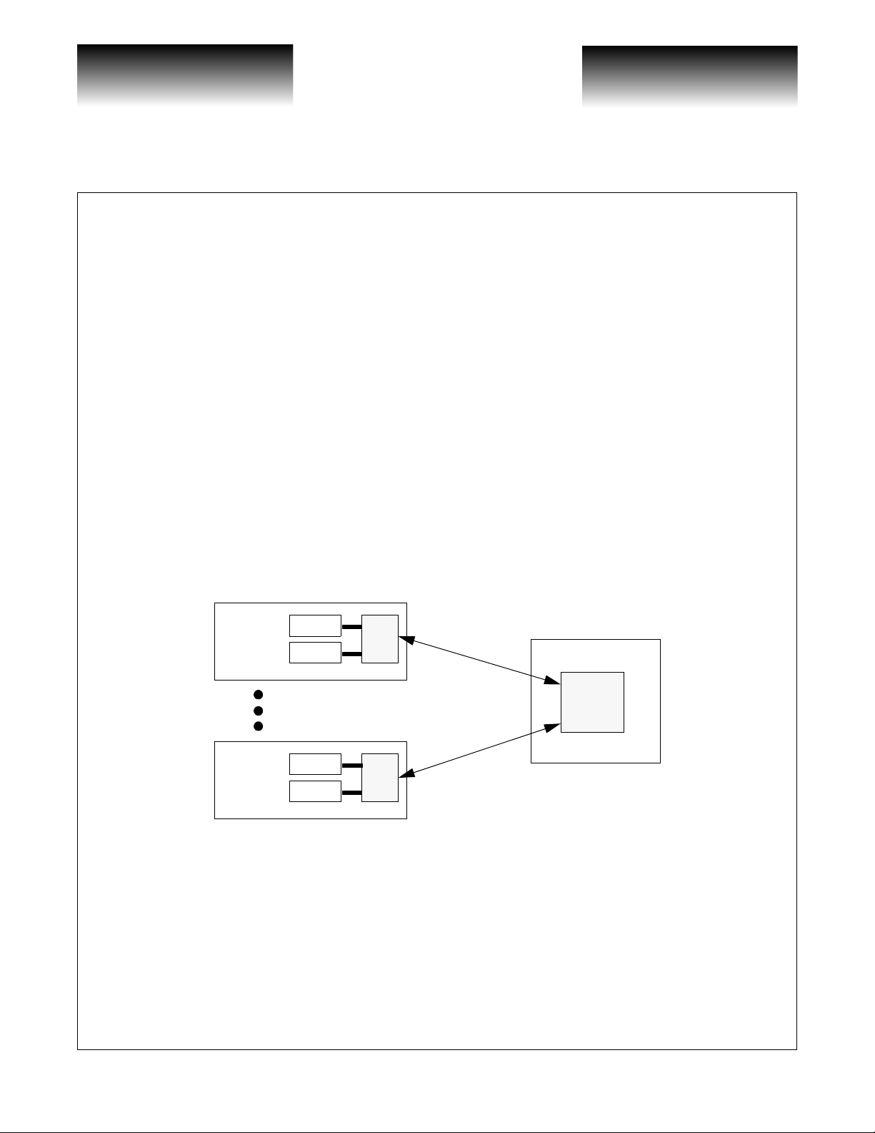
2.0 Packet Mode
2.1 Overview
In Packet Mode the BYPASS signal is set LOW to allow t he transceiver to utilize the built-in retransmission,
camp-on, virtual output queue and delayed read enable logic. In addition, the signal CELLSYN is held LOW to
disable the cell synchronization process. A special command word can be sent through the transceiver to the switch
chip requesting connection to one or multiple output ports. Acknowledge (ACK) in formation will be returned to th e
transceiver from the switch allowing the port card t o start transm itting data (see Application Note 31: Des ign Guide
for a Packet Based Switch with Distributed Control). This special command word, a Connection Request (CRQ)
Command, can be put on the front of the data packet to make the packet self routing. In this mode of operation, no
controller chip needs to be connected to the switch chip as the switch chip handles all arbitr ation for connection
requests (see the VSC880 data sheet). If the system designer wants to by pass the features des cribed in this section, the
signal BYPASS can be set HIGH. The user will then have direct control of the data stream between the transceiver
and the switch. A picture of a Packet Mode system is shown below. The minimum packet size in this mode of
operation is 4 words or 16 bytes.
Data Sheet
Figure 1: Packet Mode System
Port Card
Port Card
TXFIFO
RXFIFO
TXFIFO
RXFIFO
Trans
Switch Card
VSC870
Switch
Chip
VSC880
Trans
VSC870
2.2 Data Encoding Format
The data and command words are described in section 1.0. In this section the Connection Request (CRQ) word
format at 4 interfaces (transceiver parallel transmit port, serial line to switch, serial line from switch and transceiver
parallel receive port) is described. In this mode the TXTYP[1:0] and RXTYP[1:0] bits are encoded differently than
the overhead bits (B[1:0]) to effectively support a vari ety of featu res in the Packet Mode. The enco ding for these data
types are described in the following section.
Page 12 G52190-0, Rev 4.1
© VITESSE SEMICONDUCTOR CORPORATION • 741 Ca l le Pl an o • Camarillo, CA 93012
Tel: (800) VITESSE • FAX: (805) 987-5896 • Email: prodinfo@vitesse.com
Internet: www.vitesse.com
01/05/01
 Loading...