


VITESSE VSC852TP Datasheet
VITESSE
SEMICONDUCTOR CORPORATION
Data Sheet
VSC852
1.6Gb/s 64x64
Crosspoint Switch
G52245-0, Rev 4.1 Page 1
9/26/00
© VITESSE SEMICONDUCTOR CORPORATION • 741 Calle Plano • Camarillo, CA 93012
Tel: (800)-VITESSE • FAX: (805) 987-5896 • Email: prodinfo@vitesse.com
Internet: www.vitesse.com
Features
General Description
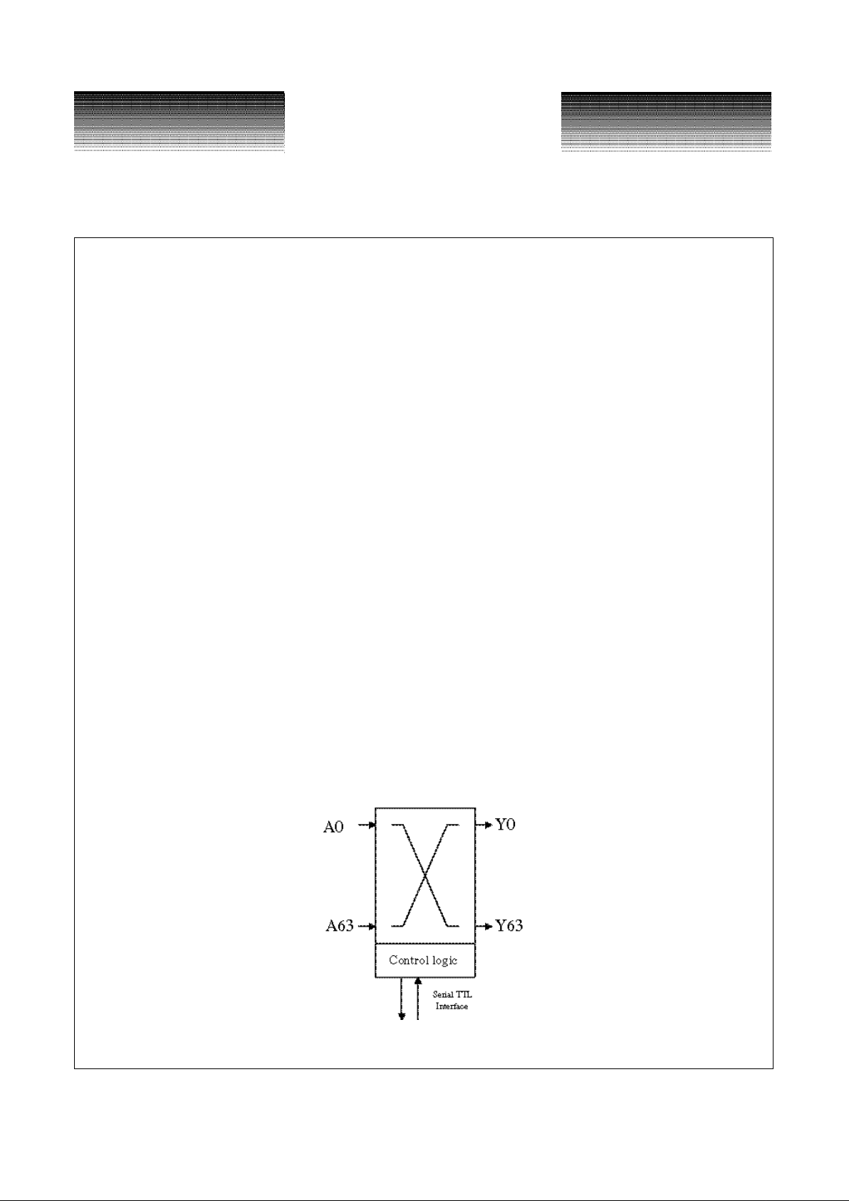
The VSC852 is a monolithic 64x64 asynchronous crosspoint switch, designed to carry broadband data
streams up to 1.6Gb/s. Typical applications include Gigabit Fibre Channel/Ethernet and HDTV. The nonblocking switch core is programmed through a serial port interface that allows random access programming of
each output port. A high degree of signal integrity is maintained throughout the chip via fully differential signal
paths.
The crosspoint function is based on a multiplexer tree architecture. Each data output is driven by a 64:1
multiplexer tree that can be programmed to one and only one of its 64 inputs. The signal path is unregistered, so
no clock is required for the data inputs. The signal path is asynchronous, so there are no restrictions on the
phase, frequency, or signal pattern at each input. (Note: the maximum frequency for any data line is 1.6Gb/s.)
Each output driver is a fully differential switched current driver with on-die back-terminations for maximum signal integrity. Data inputs are terminated on die through 50Ω resistors to an external VTT supply.
The serial port interface uses TTL levels and provides separate pins for data input and output. Core programming can be sequential for each address or multiple program assignments can be queued and issued simultaneously.
VSC852 Block Diagram
• 64 Input by 64 Output Non-Blocking
• Full Broadcast/Multicast Capability
• 1.6Gb/s NRZ Data Bandwidth
• Designed for HDTV, GE, and FC
• TTL-Compatible Control I/O
• Fully Differential Data Path, PECL-Compatible
• On-Chip Input Terminations
• Single 3.3V Supply, 28W Maximum Dissipation
• High Performance 35mm, 440 BGA Package
VITESSE
SEMICONDUCTOR CORPORATION
Datasheet
VSC852
1.6Gb/s 64x64
Crosspoint Switch
Page 2 G52245-0, Rev 4.1
9/26/00
© VITESSE SEMICONDUCTOR CORPORATION • 741 Calle Plano • Camarillo, CA 93012
Tel: (800)-VITESSE • FAX: (805) 987-5896 • Email: prodinfo@vitesse.com
Internet: www.vitesse.com
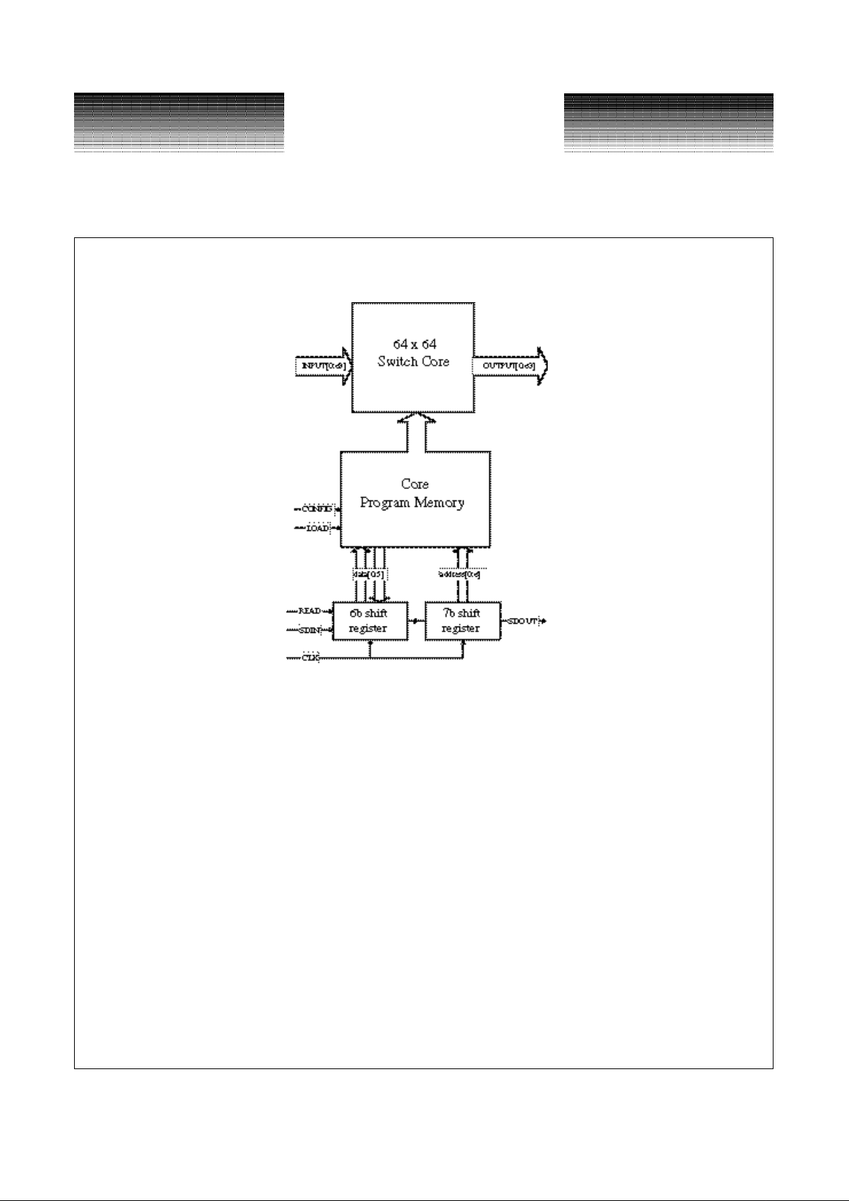
Functional Diagram
Functional Description
Input/Output Characteristics
All input data must be differential and biased to PECL levels. On-chip terminations are provided, with a
nominal impedance of 50Ω. All input termination resistors are tied to V
TERM
. To minimize power dissipation,
the V
TERM
supply should be biased within ±100mV of the input common-mode voltage (nominally 2.0V). The
V
TERM
supply can be biased below the input common-mode voltage at the expense of increased on-chip power
dissipation.
Data outputs are provided through differential current switches with on-chip back-terminations. The drive
level of the output circuit is designed to handle external 50Ω termination. Although external termination is not
required for correct functional operation, it is strongly recommended to assure proper signal levels and minimize reflections.
Programming Interface
The switch core is programmed through a serial interface circuit that allows sequential reads or writes to
the program memory array. The program memory array is buffered to allow multiple programming instructions
to be loaded simultaneously with the CONFIG pin.
The program data is composed of two parts: output pin address and input pin address. The output pin
address, denoted by A0 through A6, specifies which output channel is to be programmed. Address bit A6 is
reserved for future expansion. The input pin address, denoted by D0 through D5, specifies which input port the
VITESSE
SEMICONDUCTOR CORPORATION
Data Sheet
VSC852
1.6Gb/s 64x64
Crosspoint Switch
G52245-0, Rev 4.1 Page 3
9/26/00
© VITESSE SEMICONDUCTOR CORPORATION • 741 Calle Plano • Camarillo, CA 93012
Tel: (800)-VITESSE • FAX: (805) 987-5896 • Email: prodinfo@vitesse.com
Internet: www.vitesse.com
switch slice should connect to. The format of the program data is simple binary, where the binary value maps
directly to the switch slice position and/or input port number. For example, program data 0000100/010110
would direct output channel Y4 to connect to input channel A22.
To program the switch core, the address and data (13 bits total) for the given output port must be serially
clocked into the SDIN input. The LOAD pin must be asserted with the last serial program bit to load the program data into the on-chip program register. The program data will be held in the register until it is either reprogrammed or the chip is powered off. The last step to programming the switch core is to transfer the program
data to the registers that control the state of each switch slice. The transfer is completed by asserting the CONFIG pin. The CONFIG pin can be used as a strobe to allow multiple program commands to be implemented
simultaneously. The CONFIG pin can also be tied HIGH (always asserted) so the core will reprogram after
every LOAD pulse. See Figure 1.
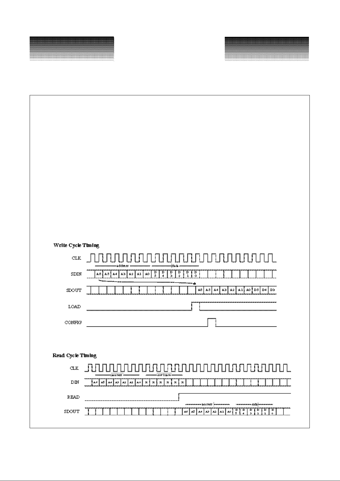
To read the current programming of the switch core, the desired address to query must be clocked into the
chip’s SDIN port. The format of the program data is the same as for writing. Because of the depth of the on-chip
registers, the address bits must be followed by another 6 CLK cycles so the address data is correctly positioned
in the internal register. The dummy bits that are clocked in during the last 6 bits of the program data will be
overwritten when READ is asserted. As the last dummy bit is clocked in, the READ pin must be asserted to
load the on-chip program data into the shift register used for the serial interface logic. See Figure 2.
Figure 1: Write Sequence Timing
Figure 2: Read Sequence Timing
VITESSE
SEMICONDUCTOR CORPORATION
Datasheet
VSC852
1.6Gb/s 64x64
Crosspoint Switch
Page 4 G52245-0, Rev 4.1
9/26/00
© VITESSE SEMICONDUCTOR CORPORATION • 741 Calle Plano • Camarillo, CA 93012
Tel: (800)-VITESSE • FAX: (805) 987-5896 • Email: prodinfo@vitesse.com
Internet: www.vitesse.com
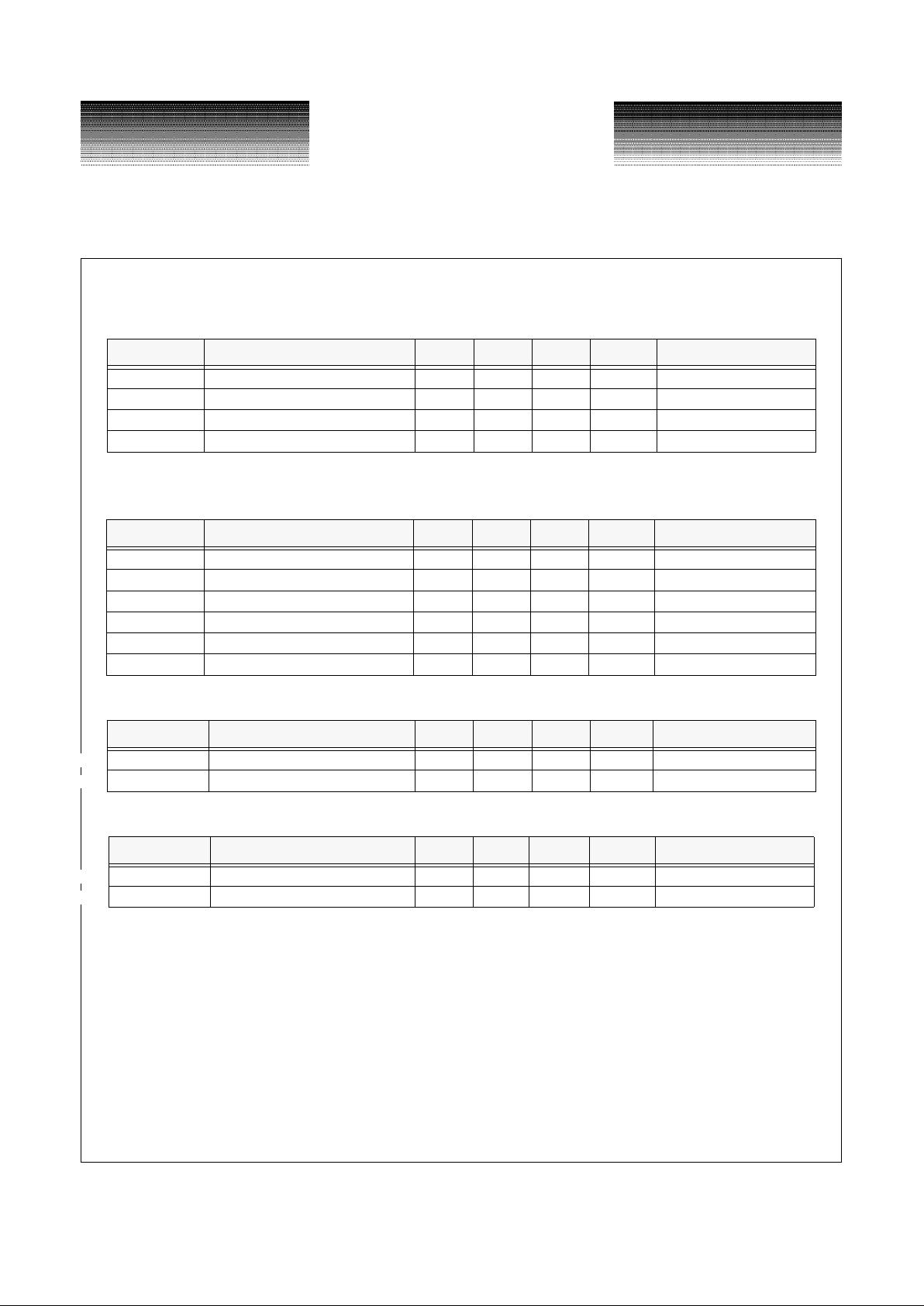
DC Characteristics (All characteristics are over the specified operating conditions)
Table 1: Power
NOTE: Specified with outputs terminated with 50Ω to +2.0V.
Table 2: Program Input Levels (TTL)
Table 3: Data Input Levels (Differential PECL)
Table 4: Data Output Levels (Differential PECL)
NOTE: (1) V
CC
= V
CCP
= 3.3V, V
EE
= 0V.
Parameter Description Min Typ Max Units Conditions
I
CC
VCC supply current — — 5400 mA
I
CCP
V
CCP
supply current — — 2600 mA
I
TERM
V
TERM
supply current — — ±512 mA VIN = 2.4V
P
T
Total chip power (I
TERM
= 0) — — -500 µA VIN = 0.5V
Parameter Description Min Typ Max Units Conditions
V
IH
Input HIGH voltage 2.0 — 3.5 V —
V
IL
Input LOW voltage 0 — 0.8 V —
I
IH
Input HIGH current — — 500 µA VIN = 2.4V
I
IL
Input LOW current — — -500 µA VIN = 0.5V
V
OH
Output HIGH voltage 2.4 --- --- V IOH = -2mA
V
OL
Output LOW voltage --- --- 0.4 V IOL = 2mA
Parameter Description Min Typ Max Units Conditions
V
ID
Input differential voltage 400 — 1000 mV single-ended measurement
V
ICM
Input common-mode voltage 1.8 — 2.3 V V
TERM
= V
CC
-1.3V
Parameter Description Min Typ Max Units Conditions
V
OD
Output differential voltage 600 — 1000 mV See Note 1
V
OCM
Output common-mode voltage 1.8 — 2.3 V See Note 1
VITESSE
SEMICONDUCTOR CORPORATION
Data Sheet
VSC852
1.6Gb/s 64x64
Crosspoint Switch
G52245-0, Rev 4.1 Page 5
9/26/00
© VITESSE SEMICONDUCTOR CORPORATION • 741 Calle Plano • Camarillo, CA 93012
Tel: (800)-VITESSE • FAX: (805) 987-5896 • Email: prodinfo@vitesse.com
Internet: www.vitesse.com
AC Characteristics
Table 5: Data Path
NOTE: (1) Tested on sample basis only.
Table 6: Program Interface
NOTE: (1) 20pF load.
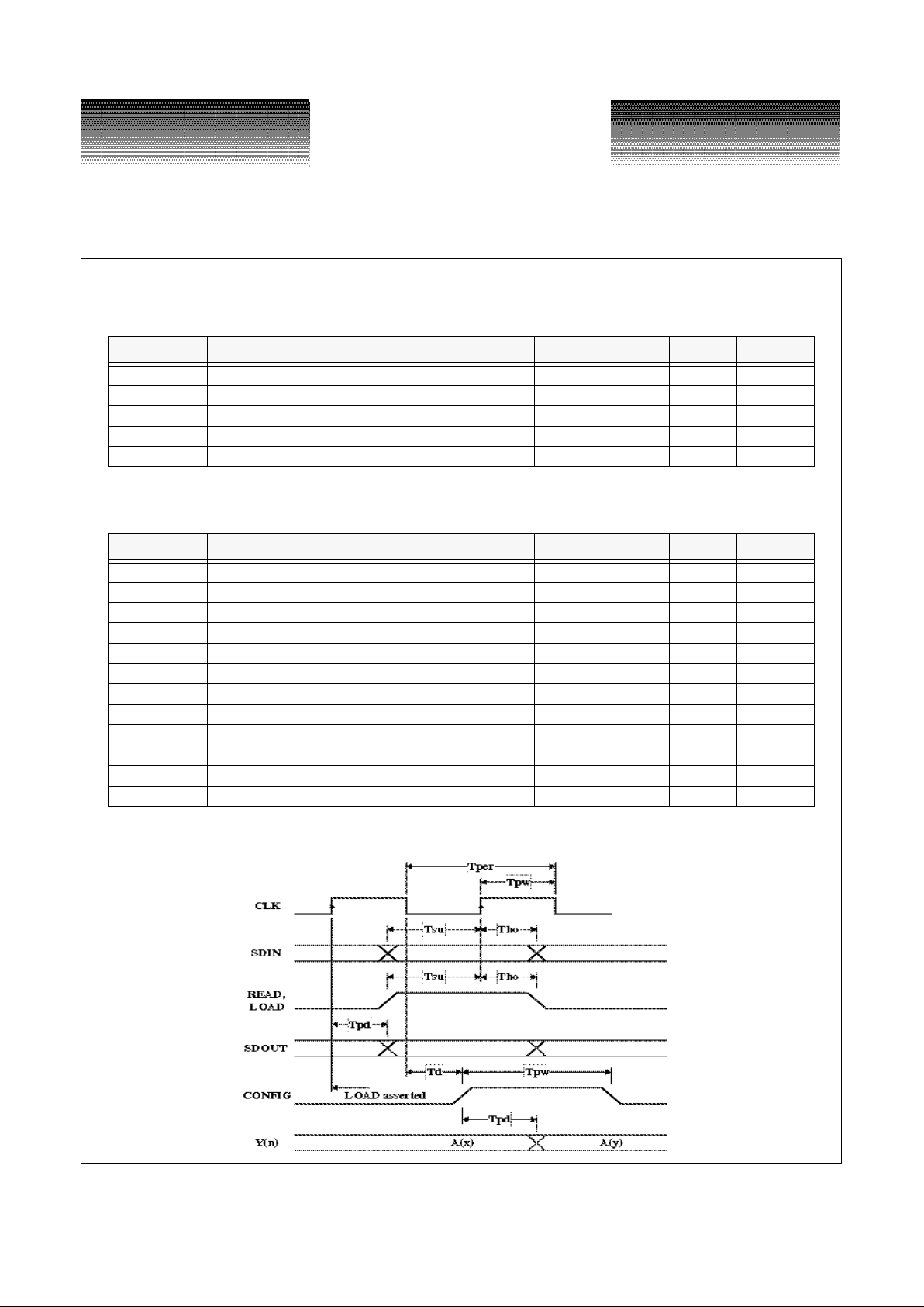
Figure 3: AC Timing Diagram
Parameter Description Min Typ Max Units
F
RATE
Data rate 1.6 Gb/s
T
SKW
Channel-to-channel delay skew
(1)
- 1 - ns
tR, t
F
High-speed input rise/fall times, 20% to 80% 250 ps
tR, t
F
High-speed output rise/fall times, 20% to 80% - - 250 ps
t
jP
Output delay jitter, peak-peak
(1)
100 ps
Parameter Description Min Typ Max Units
T
PER(CLK)
Serial clock period 40 ns
T
PW(CLK)
Serial clock pulse width 16 ns
T
SU(SDIN)
Serial data input setup time 2 ns
T
HO(SDIN)
Serial data input hold time 2 ns
T
SU(READ)
READ pulse setup time 2 ns
T
HO(READ)
READ pulse hold time 2 ns
T
SU(LOAD)
LOAD pulse setup time 2 ns
T
HO(LOAD)
LOAD pulse hold time 2 ns
T
PD(SDOUT)
Serial data output propagation delay
(1)
10 ns
T
D(CONFIG)
Configuration pulse delay time 3 ns
T
PW(CONFIG)
Configuration pulse width 30 ns
T
PD(CONFIG)
Configuration delay 5 ns