

Page 1

VITESSE SEMICONDUCTOR CORPORATION
Page 1
10/21/99 741 Calle Plano, Camarillo, CA 93012 • 805/388-3700 • FAX: 805/987-5896
VITESSE
SEMICONDUCTOR CORPORATION
Data Sheet
SC851
1.6 Gb/s 32 X 32
Crosspoint Switc
h
G52167-0 Rev. 4.1
Features
General Description
This VSC851 is a 32 x 32 crosspoint switch intended for high speed digital data communications applications. This product has 32 dat a inp uts and 32 data output s. An y inpu t c an be mul tiple x ed to any, some, or all outputs. High speed digital data up to 1.6Gb/s can be switched with less than 150pS pulse width distortion. In
broadcast mode, any two outputs will exhibit less than 250pS of skew relative to one another. Signals in data
paths are fully differential to minimize duty cycle distortion. The V SC851 requir es both -2V and 3.3V power
supplies.
The address signals that control traf f ic pat terns for data pa ths are double b uffered. the LSTROBE signal load
individual addresses for each output. The GSTROBE signal is used to update addresses for all 32 outputs simul-
taneously. This method allows users to configure any, som e or all switches indepen dently without disrup ting
data flow of the data paths. Broadcast and flow through function ality are controlled via BROADCAST and
FLOWTHRU inputs.
This product is ideal for high speed digital applications including Gigabit Ethernet and ATM switch cores,
data distribution for telecommunica tions, fiber channel networkin g, computer networking, mu ltiprocessor
switching, and test equipment. In a telecommunications SONET application, for example, the VSC851 can be
used as an STS-12 protection switch.
The VSC851 is packaged in a 256 pin thermally enhanced LDCC package. This product is fabricated using
Vitesse’s E/D GaAs MESFET process which achieves high speed coupled with low power dissipation.
Functional Description
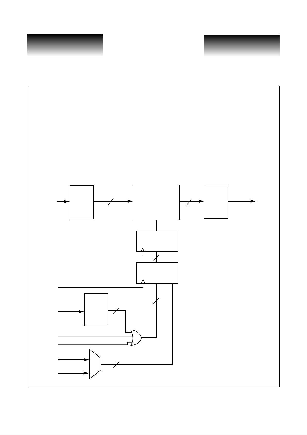
The VSC851 may be used t o conn ect any one of 32 inputs t o any one or combination of 32 output channel s,
according to a user defined bit pattern stored in each output channel’s control latches (see Figure 1). For data
path operation, signals flow transparently from inputs I+/I-[0:31] to output channels Z+/Z-[0:31] thro ugh
thirty-two 32:1 multiplexers. The traffic pattern is controlled by data previously stored in thirty-two 5-bit control latches each corresponding to an output channel. Value of these 5-bit control latches is a binary numerical
representation of the input channel selected. D[4:0] = 00000 corresponds to I[0], D[4:0] = 00001 corresponds
to I[1], etc. Similarly, A [4:0] = 00000 selects path to output Z [0], A [4:0] = 00001 to Z [1], etc. To configure
the switch, at rising edge of LSTROBE, the bank of holding registers for a particular ch annel i s upd at ed by input
addresses D[4:0] which describes a new path for that channe l. After some or all ho lding registers are programmed, a high pulse is applied to GSTROBE to transfer the in fo rmation from holding registers into all control
latches. By this method, the entire crosspoint switch can be reconfigured simultaneously.
• 1.6Gb/s Operation
• Non-blocking Architecture
• Duty-cycle Distortion: ≤ 150pS
• ≤ 2nS Propagation Delay for Data Path
• ≤ 250pS Output to Output Skew in Broadcast Mode
• Power Supply: -2 V and 3.3 V
• ECL Differential Data Paths
• 3.3 V TTL Control Signals
• Low Power Dissipation
• Package: 256-pin LDCC
Page 2
VITESSE
SEMICONDUCTOR CORPORATION
Data Shee
t
VSC851
.6 Gb/s 32x32
rosspoint Switch
Page 2
VITESSE SEMICONDUCTOR CORPORATION
741 Calle Plano, Camarillo, CA 93012 • 805/388-3700 • FAX: 805/987-5896 10/21/99
G52167-0 Rev. 4.1
32 x 32
Switch Matrix
GSTROBE
Input
Buffers
Output
Buffers
32 x 32
Control Latches
32 x 5
Holding Registers
LSTROBE
A [4:0]
5 to 32
Decode
BROADCAST
FLOWTHRU
D [4:0]
0,1......31
160
64
64
32
32
5
Z + [0:31]
Z - [0:31]
I + [0:31]
I - [0:31]
The VSC851 can be configured in Broadcast mode. In Broadcast Mode, at the rising edge of LSTROBE, all
holding registe rs are up dat ed b y input addresses D[4:0]. If a high pulse is appli ed to GSTROBE, the entire crosspoint is configured and the selected data are broadcasted to all of the outputs.
In FlowThru mode, at the rising edge of LSTROBE, all holdin g re g isters are set to t he n umerical represent a-
tion of the output which th ey control, (i.e., 00000 is loaded for outp ut Z[0], 00001 is loaded for output Z[1]
etc.). If a high pulse is then applied to GSTROBE, these values are passed to the contro l latch es. In this mode ,
data from I[0] is switched to Z[0] da ta from I[1] is switched to Z[1] , etc. The input address values at D[4:0]
and the output address values at A[4:0] are ignored in FlowThru Mode. All data input and output signals (I+/I-
[0:31], Z+/Z-[0:31]) are differential ECL levels. All other signals are TTL levels. If both BROADCAST and
FLOWTHRU inputs are asserted, the FlowThru Mode overrides the Broadcast Mode.
VSC851 Block Diagram
Page 3
VITESSE SEMICONDUCTOR CORPORATION
Page 3
10/21/99 741 Calle Plano, Camarillo, CA 93012 • 805/388-3700 • FAX: 805/987-5896
VITESSE
SEMICONDUCTOR CORPORATION
Data Sheet
SC851
1.6 Gb/s 32 X 32
Crosspoint Switc
h
G52167-0 Rev. 4.1
AC Characteristics
(Over recommended operating conditions. ECL Output load 50Ω to V
TT.
)
Table 1: Data Flow Mode.
(1) Duty cycle distortion = duty cycle out - duty cycle in (pS). With 8B/10B encoded data.
AC Timing Waveforms
Figure 1: Normal Data Flow Timing
Parameters Description Min Typ Max Units Conditions
T
PW
Minimum input pulse width 640 — — pS Worst case 60/40 input duty cycle
T
DLY
Propagation delay 600 — 2000 pS —
Tduty Duty cycle distortion — — 150 p S at 1.6 Gb/s Note(1)
Tskew Output to output skew — — 250 pS On a given part broadcast mode
Tpskew Data path skew — — 500 pS
For any 2 paths from I+/I- to Z+/Z- on
a given part
Minimum Input Pulse Width & Propagation Delay
T
DLY
T
PW
I+ [0:31]
I-[0:31]
Z+ [0:31]
Z-[0:31]
T
DLY
T
SKEW
T
SKEW
Page 4
VITESSE
SEMICONDUCTOR CORPORATION
Data Shee
t
VSC851
.6 Gb/s 32x32
rosspoint Switch
Page 4
VITESSE SEMICONDUCTOR CORPORATION
741 Calle Plano, Camarillo, CA 93012 • 805/388-3700 • FAX: 805/987-5896 10/21/99
G52167-0 Rev. 4.1
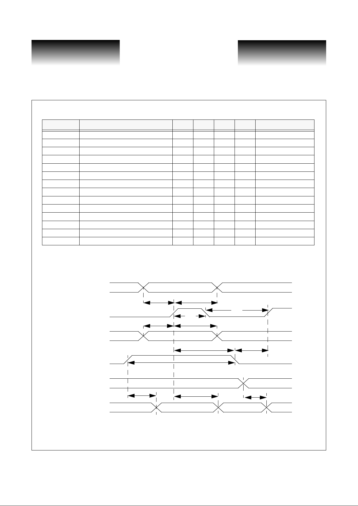
Table 2: Configuration, Broadcast, FlowThru Mode.
Figure 2: Configuration Mode Timing
Parameters Description Min Typ Max Units Conditions
T
LSW
LSTROBE pulse width 5 ——nS—
T
GSW
GSTROBE pulse width 5 — — nS —
T
GSZ
GSTROBE to Z+/Z- Outputs Delay 1.5 — 5.0 nS —
T
LSZ
LSTROBE to Z+/Z- Outputs Delay 2 — 6.0 nS GSTROBE high
T
ALSSU
A[4:0] to LSTROBE setup time 3.5 — — nS —
T
ALSH
A[4:0] to LSTROBE hold time 1 — — nS —
T
DLSSU
D[4:0] to LSTROBE setup time 3.5 — — nS —
T
DLSH
D[4:0] to LSTROBE hold time 1 — — nS —
T
GLSU
GSTROBE to LSTROBE setup time 2.5 — — nS —
T
GLH
GSTROBE to LSTROBE hold time 2 — — nS —
T
BLSSU
BROADCAST to LSTROBE setup time 4 — — nS —
T
BLSH
BROADCAST to LSTROBE hold time 1 — — nS —
T
FLSSU
FLOWTHRU to LSTROBE setup time 4 — — nS —
T
FLSH
FLOWTHRU to LSTROBE hold time 1 — — nS —
I+ [0:15]
I- [0:15]
Z+ [0:31]
Z- [0:31]
A[0:4]
T
LSW
T
DLSSU
T
DLSH
T
ALSSU
T
ALSH
T
GLSU
T
GSZ
T
GLH
(Output Address )
D[0:4]
(Input Address)
LSTROBE
GSTROBE
T
LSW
T
LSZ
T
DLY
T
GSW
Page 5
VITESSE SEMICONDUCTOR CORPORATION
Page 5
10/21/99 741 Calle Plano, Camarillo, CA 93012 • 805/388-3700 • FAX: 805/987-5896
VITESSE
SEMICONDUCTOR CORPORATION
Data Sheet
SC851
1.6 Gb/s 32 X 32
Crosspoint Switc
h
G52167-0 Rev. 4.1
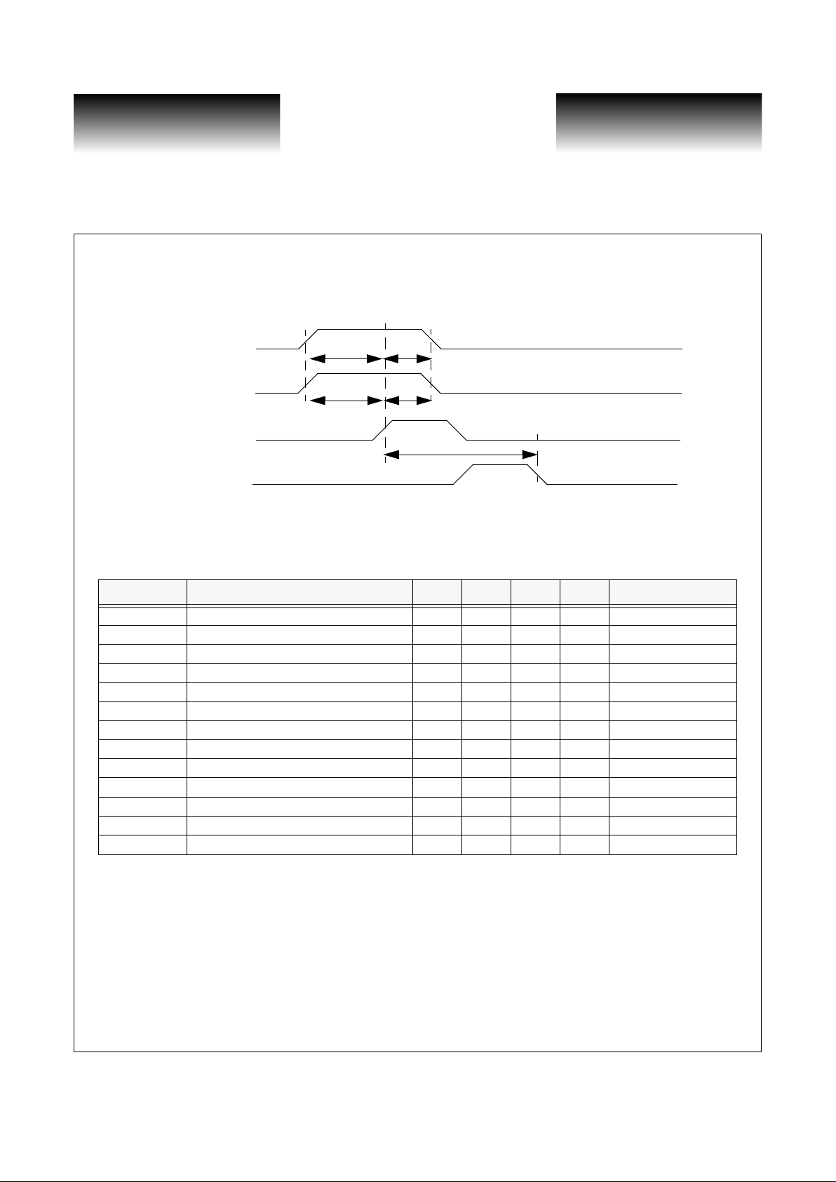
Figure 3: Broadcast and FlowThru Timing
DC Characteristics
(Over recommended operating conditions. ECL Output load 50W to V
TT.
)
Parameters Description Min Typ Max Units Conditions
V
ODIF
Differential ECL Output Voltage 600 —1100mV50Ω to VTT
V
OCM
Common Mode ECL Output Voltage -1.5 — -1.0 V 50Ω to VTT
V
IDIF
Differential ECL Input Voltage 20 0 — 1200 mV
V
ICM
Common Mode ECL Input Voltage -1.5 — -0.5 V
I
IHE
Input HIGH ECL Current — — +200 µAV
IN =
-0.7V
I
ILE
Input LOW ECL Current -50 — — µAV
IN =
-2.0V
V
IHT
Input HIGH voltage (TTL) 2.0 — 4.3 V
V
ILT
Input LOW voltage (TTL) 0 — 0.8 V
I
IHT
Input HIGH current (TTL) — 50 — µA 2.0V < VIN < 4.3V
I
ILT
Input LOW current (TTL) -500 — — µA -0.5V < VIN < 0.8V
I
VTTL
VTTL Supply Current — — 20 mA
I
VTT
VTT Supply Current — — 3600 mA Outputs open
P
D
Power dissipation — — 7500 mW
T
BLSSU
T
BLSH
FLOWTHRU
GSTROBE
BROADCAST
LSTROBE
T
FLSSU
T
FLSH
T
GLSU
Page 6

VITESSE
SEMICONDUCTOR CORPORATION
Data Shee
t
VSC851
.6 Gb/s 32x32
rosspoint Switch
Page 6
VITESSE SEMICONDUCTOR CORPORATION
741 Calle Plano, Camarillo, CA 93012 • 805/388-3700 • FAX: 805/987-5896 10/21/99
G52167-0 Rev. 4.1
Absolute Maximum Ratings
(1)
ECL Power Supply Voltage , VTT potential to GND.......................................................................-2.5V to +0.5V
TTL Power Supply Voltage , V
TTL
potential to GND.....................................................................-0.5V to +4.3V
ECL input Voltage Applied, V
ECLIN
.......................................................................................VTT-0.5V to +0.5V
TTL input Voltage Applied, V
TTLIN
.....................................................................................-0.5V to V
TTL
+1.0V
Output Current, I
OUT
,(DC, output HI).........................................................................................................50 mA
Case Temperature Under Bias, TC..................................................................................................-55° to +125°C
Storage Temperature (ambient), TSTG........................................................................................-65°C to +150°C
Recommended Operating Conditions
ECL Supply Voltage, VTT......................................................................................................................-2.0V ± 5%
TTL Supply Voltage, V
TTL
.....................................................................................................................3.3V ± 5%
Commercial Operating Temperature Range, T(2)..................................................................................0° to 70°C
NOTES: (1) CAUTION: Stresses listed under "Absolute Maximum Ratings" may be applied to devices one at a time without caus-
ing permanent damage. Functionality at or above the values listed is not implied. Exposure to these values for extended
periods may affect device reliability.
(2) Lower limit of specification is ambient temperature and upper limit is case temperature.
Page 7

VITESSE SEMICONDUCTOR CORPORATION
Page 7
10/21/99 741 Calle Plano, Camarillo, CA 93012 • 805/388-3700 • FAX: 805/987-5896
VITESSE
SEMICONDUCTOR CORPORATION
Data Sheet
SC851
1.6 Gb/s 32 X 32
Crosspoint Switc
h
G52167-0 Rev. 4.1
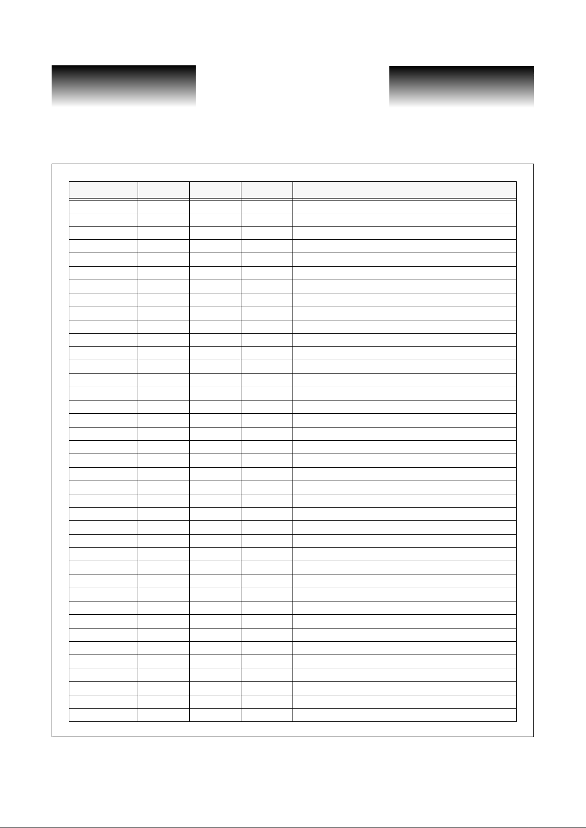
Table 3: Package Pin Identification
Signal Pin I/O Level Pin Description
VTT 1 P -2V -2.0V power supply
VCC 2 P GND Ground
N/C 3 No connection
N/C 4 No connection
N/C 5 No connection
VTTL 6 P +3.3V +3.3V power supply
N/C 7 No connection
N/C 8 No connection
N/C 9 No connection
N/C 10 No connection
VTTL 11 P +3. 3V +3.3V po w e r su pp ly
N/C 12 No connection
N/C 13 No connection
Z15 14 O ECL Serial data out
ZN15 15 O ECL Serial data out
VTT 16 P -2V -2.0V power supply
VCC 17 P GND Ground
VTTL 18 P +3.3V +3.3V power su pp ly
N/C 19 No connection
Z14 20 O ECL Serial data out
ZN14 21 O ECL Serial data out
Z13 22 O ECL Serial data out
ZN13 23 O ECL Serial data out
VCC 24 P GND Ground
Z12 25 O ECL Serial data out
ZN12 26 O ECL Serial data out
Z11 27 O ECL Serial data out
ZN11 28 O ECL Serial data out
VCC 29 P GND Ground
Z10 30 O ECL Serial data out
ZN10 31 O ECL Serial data out
VTT 32 P -2V -2.0V power supply
VCC 33 P GND Ground
Z9 34 O ECL Serial data out
ZN9 35 O ECL Serial data out
VCC 36 P GND Ground
Z8 37 O ECL Serial data out
Page 8

VITESSE
SEMICONDUCTOR CORPORATION
Data Shee
t
VSC851
.6 Gb/s 32x32
rosspoint Switch
Page 8
VITESSE SEMICONDUCTOR CORPORATION
741 Calle Plano, Camarillo, CA 93012 • 805/388-3700 • FAX: 805/987-5896 10/21/99
G52167-0 Rev. 4.1
ZN8 38 O ECL Serial data out
Z7 39 O ECL Serial data out
ZN7 40 O ECL Serial data out
VCC 41 P GND Ground
Z6 42 O ECL Serial data out
ZN6 43 O ECL Serial data out
Z5 44 O ECL Serial data out
ZN5 45 O ECL Serial data out
N/C 46 No connection
VCC 47 P GND Ground
VTT 48 P -2V -2.0V power supply
VCC 49 P GND Ground
Z4 50 O ECL Serial data out
ZN4 51 O ECL Serial data out
Z3 52 O ECL Serial data out
ZN3 53 O ECL Serial data out
VCC 54 P GND Ground
Z2 55 O ECL Serial data out
ZN2 56 O ECL Serial data out
Z1 57 O ECL Serial data out
ZN1 58 O ECL Serial data out
VCC 59 P GND Ground
Z0 60 O ECL Serial data out
ZN0 61 O ECL Serial data out
I0 62 I ECL Serial data in
VTT 63 P -2V -2.0V power supply
VCC 64 P GND Ground
IN0 65 I ECL Serial data in
I1 66 I ECL Serial data in
IN1 67 I ECL Serial data in
VCC 68 P GND Ground
VTT 69 P -2V -2.0V power supply
VCC 70 P GND Ground
N/C 71 No connection
I2 72 I ECL Serial data in
IN2 73 I ECL Serial data in
I3 74 I ECL Serial data in
IN3 75 I ECL Serial data in
I4 76 I ECL Serial data in
Signal Pin I/O Level Pin Description
Page 9

VITESSE SEMICONDUCTOR CORPORATION
Page 9
10/21/99 741 Calle Plano, Camarillo, CA 93012 • 805/388-3700 • FAX: 805/987-5896
VITESSE
SEMICONDUCTOR CORPORATION
Data Sheet
SC851
1.6 Gb/s 32 X 32
Crosspoint Switc
h
G52167-0 Rev. 4.1
IN4 77 I ECL Serial data in
I5 78 I ECL Serial data in
IN5 79 I ECL Serial data in
I6 80 I ECL Serial data in
IN6 81 I ECL Serial data in
N/C 82 No connection
I7 83 I ECL Serial data in
IN7 84 I ECL Serial data in
I8 85 I ECL Serial data in
IN8 86 I ECL Serial data in
VTT 87 P -2V -2.0V power supply
VCC 88 P GND Ground
I9 89 I ECL Serial data in
IN9 90 I ECL Serial data in
I10 91 I ECL Serial data in
IN10 92 I ECL Serial data in
I11 93 I ECL Serial data in
IN11 94 I ECL Serial data in
I12 95 I ECL Serial data in
IN12 96 I ECL Serial data in
I13 97 I ECL Serial data in
IN13 98 I ECL Serial data in
I14 99 I ECL Serial data in
IN14 100 I ECL Serial data in
I15 101 I ECL Serial data in
IN15 102 I ECL Serial data in
I16 103 I ECL Serial data in
IN16 104 I ECL Serial data in
VTT 105 P -2.0V -2.0V power supply
VCC 106 P GND Ground
I17 107 I ECL Serial data in
IN17 108 I ECL Serial data in
I18 109 I ECL Serial data in
IN18 110 I ECL Serial data in
N/C 111 No connection
I19 112 I ECL Serial data in
IN19 113 I ECL Serial data in
I20 114 I ECL Serial data in
IN20 115 I ECL Serial data in
Signal Pin I/O Level Pin Description
Page 10
VITESSE
SEMICONDUCTOR CORPORATION
Data Shee
t
VSC851
.6 Gb/s 32x32
rosspoint Switch
Page 10
VITESSE SEMICONDUCTOR CORPORATION
741 Calle Plano, Camarillo, CA 93012 • 805/388-3700 • FAX: 805/987-5896 10/21/99
G52167-0 Rev. 4.1
I21 116 I ECL Serial data in
IN21 117 I ECL Serial data in
I22 118 I ECL Serial data in
IN22 119 I ECL Serial data in
I23 120 I ECL Serial data in
IN23 121 I ECL Serial data in
N/C 122 No connection
VTT 123 P -2V -2.0V power supply
VCC 124 P GND Ground
VCC 125 P GND Ground
I24 126 I ECL Serial data in
IN24 127 I ECL Serial data in
I25 128 I ECL Serial data in
VTT 129 P -2V -2.0V power supply
VCC 130 P GND Ground
IN25 131 I ECL Serial data in
I26 132 I ECL Serial data in
IN26 133 I ECL Serial data in
VCC 134 P GND Ground
I27 135 I ECL Serial data in
IN27 136 I ECL Serial data in
I28 137 I ECL Serial data in
IN28 138 I ECL Serial data in
VCC 139 P GND Ground
I29 140 I ECL Serial data in
IN29 141 I ECL Serial data in
I30 142 I ECL Serial data in
IN30 143 I ECL Serial data in
VTT 144 P -2V -2.0V power supply
VCC 145 P GND Ground
VCC 146 P GND Ground
N/C 147 No connection
I31 148 I ECL Serial data in
IN31 149 I ECL Serial data in
Z31 150 O ECL Serial data out
ZN31 151 O ECL Serial data out
VCC 152 P GND Ground
Z30 153 O ECL Serial data out
ZN30 154 O ECL Serial data out
Signal Pin I/O Level Pin Description
Page 11

VITESSE SEMICONDUCTOR CORPORATION
Page 11
10/21/99 741 Calle Plano, Camarillo, CA 93012 • 805/388-3700 • FAX: 805/987-5896
VITESSE
SEMICONDUCTOR CORPORATION
Data Sheet
SC851
1.6 Gb/s 32 X 32
Crosspoint Switc
h
G52167-0 Rev. 4.1
Z29 155 O ECL Serial data out
ZN29 156 O ECL Serial data out
VCC 157 P GND Ground
Z28 158 O ECL Serial data out
ZN28 159 O ECL Serial data out
VTT 160 P -2V -2.0V power supply
VCC 161 P GND Ground
Z27 162 O ECL Serial data out
ZN27 163 O ECL Serial data out
VCC 164 P GND Ground
Z26 165 O ECL Serial data out
ZN26 166 O ECL Serial data out
Z25 167 O ECL Serial data out
ZN25 168 O ECL Serial data out
VCC 169 P GND Ground
Z24 170 O ECL Serial data out
ZN24 171 O ECL Serial data out
Z23 172 O ECL Serial data out
ZN23 173 O ECL Serial data out
N/C 174 No connection
VTTL 175 P +3.3V +3.3V power supply
VTT 176 P -2V -2.0V power supply
VCC 177 P GND Ground
Z22 178 O ECL Serial data out
ZN22 179 O ECL Serial data out
Z21 180 O ECL Serial data out
ZN21 181 O ECL Serial data out
VTTL 182 P +3.3V +3.3V power supply
Z20 183 O ECL Serial data out
ZN20 184 O ECL Serial data out
Z19 185 O ECL Serial data out
ZN19 186 O ECL Serial data out
VTTL 187 P +3.3V +3.3V power supply
Z18 188 O ECL Serial data out
ZN18 189 O ECL Serial data out
Z17 190 O ECL Serial data out
VTT 191 P -2V -2.0V power supply
VCC 192 P GND Ground
ZN17 193 O ECL Serial data out
Signal Pin I/O Level Pin Description
Page 12

VITESSE
SEMICONDUCTOR CORPORATION
Data Shee
t
VSC851
.6 Gb/s 32x32
rosspoint Switch
Page 12
VITESSE SEMICONDUCTOR CORPORATION
741 Calle Plano, Camarillo, CA 93012 • 805/388-3700 • FAX: 805/987-5896 10/21/99
G52167-0 Rev. 4.1
Z16 194 O ECL Serial data out
ZN16 195 O ECL Serial data out
VCC 196 P GND Ground
VTT 197 P -2V -2.0V power supply
VCC 198 P GND Ground
N/C 199 No connection
N/C 200 No connection
N/C 201 No connection
N/C 202 No connection
N/C 203 No connection
VSCTE 204! I -2.0 Test enable (tie to -2V)
N/C 205 No connection
N/C 206 No connection
N/C 207 No connection
N/C 208 No connection
N/C 209 No connection
N/C 210 No connection
N/C 211 No connection
N/C 212 No connection
N/C 213 No connection
N/C 214 No connection
VTT 215 P -2V -2.0V power supply
VCC 216 P GND Ground
N/C 217 No connection
N/C 218 No connection
N/C 219 No connection
A4 220 I TTL Output address
A3 221 I TTL Output address
A2 222 I TTL Output address
A1 223 I TTL Output address
A0 224 I TTL Output address
BROADCAST 225 I TTL Control signal to enable flow thru mode
FLOWTHRU 226 I TTL Control signal to enable flow thru mode
LSTROBE 227 I TTL Load addresses into holding registers
D4 228 I TTL Input address
D3 229 I TTL Input address
D2 230 I TTL Input address
D1 231 I TTL Input address
D0 232 I TTL Input address
Signal Pin I/O Level Pin Description
Page 13

VITESSE SEMICONDUCTOR CORPORATION
Page 13
10/21/99 741 Calle Plano, Camarillo, CA 93012 • 805/388-3700 • FAX: 805/987-5896
VITESSE
SEMICONDUCTOR CORPORATION
Data Sheet
SC851
1.6 Gb/s 32 X 32
Crosspoint Switc
h
G52167-0 Rev. 4.1
VTT 233 P -2V -2.0V power supply
VCC 234 P GND Ground
N/C 235 No connection
N/C 236 No connection
N/C 237 No connection
N/C 238 No connection
N/C 239 No connection
N/C 240 No connection
N/C 241 No connection
N/C 242 No connection
N/C 243 No connection
N/C 244 No connection
N/C 245 No connection
N/C 246 No connection
GSTROBE 247 I TTL
Latch enable to transfer holding register data to
control latches
N/C 248 No connection
N/C 249 No connection
N/C 250 No connection
VTT 251 P -2V -2.0V power supply
VCC 252 P GND Ground
VCC 253 P GND Ground
VSCIPNC 254* I TTL Test input (tie to -2V)
VSCOPNC 255# O ECL Test output (leave open)
N/C 256 No connection
Signal Pin I/O Level Pin Description
Page 14

VITESSE
SEMICONDUCTOR CORPORATION
Data Shee
t
VSC851
.6 Gb/s 32x32
rosspoint Switch
Page 14
VITESSE SEMICONDUCTOR CORPORATION
741 Calle Plano, Camarillo, CA 93012 • 805/388-3700 • FAX: 805/987-5896 10/21/99
G52167-0 Rev. 4.1
Package Information
*At package body.
Notes: 1) Drawing not to scale.
2) Packages: Ceramic (alumina); Heat sinks: Copper-tungsten; Leads: Alloy 42 with gold plating
Item mm (Min/Max) In (Min/Max) Item mm (Min/Max) In (Min/ Max)
A 36.57/37.59 SQ 1.440/1 .480 SQ F 0.09/0.216 0.004/0.008
B TYP 28 SQ TYP 1.1 SQ G 5.08/7.62 0.200/0.300
C* 0.51 TYP 0.020 TYP H 0.15/0.25 0.006/0.010
D 0.38/0.63 0.015/0.025 I* REF 2.54 T YP REF 0.100 TYP
E 2.16/ 2.92 0.085/0.115 J* 32.00 TYP 1.26 TYP
H
I*
C *
J *
EF
G
B
A
D
Pin 1
Heat Sink
Side
Package is
Cavity Down
Pin 256
256 LDCC Cavity Down Package
Page 15

VITESSE SEMICONDUCTOR CORPORATION
Page 15
10/21/99 741 Calle Plano, Camarillo, CA 93012 • 805/388-3700 • FAX: 805/987-5896
VITESSE
SEMICONDUCTOR CORPORATION
Data Sheet
SC851
1.6 Gb/s 32 X 32
Crosspoint Switc
h
G52167-0 Rev. 4.1
Ordering Information
VSC851-FX
Device Type:
VSC851: 32x32 Crosspoint Switch
Package Type
F: 256 LDCC
Notice
Vitesse Semiconductor Corporation reserves the right to make changes in its products, specifications or
other information at any time without prior notice. Therefore the reader is cautioned to confirm that this
datasheet is current prior to placing any orders. The company assumes no responsibility for any circuitry
described other than circuitry entirely embodied in a Vitesse product.
Warning
Vi tesse Semico ndu ctor Co rporat ion’s products are not intended for use in life supp ort appl iances, de v ices or
systems. Use of a Vitesse product in such applications without the written consent is prohibited.
Page 16

VITESSE
SEMICONDUCTOR CORPORATION
Data Shee
t
VSC851
.6 Gb/s 32x32
rosspoint Switch
Page 16
VITESSE SEMICONDUCTOR CORPORATION
741 Calle Plano, Camarillo, CA 93012 • 805/388-3700 • FAX: 805/987-5896 10/21/99
G52167-0 Rev. 4.1
 Loading...