

VITESSE VSC838UG Datasheet
VITESSE
SEMICONDUCTOR CORPORATION
Preliminary Data Sheet
VSC838
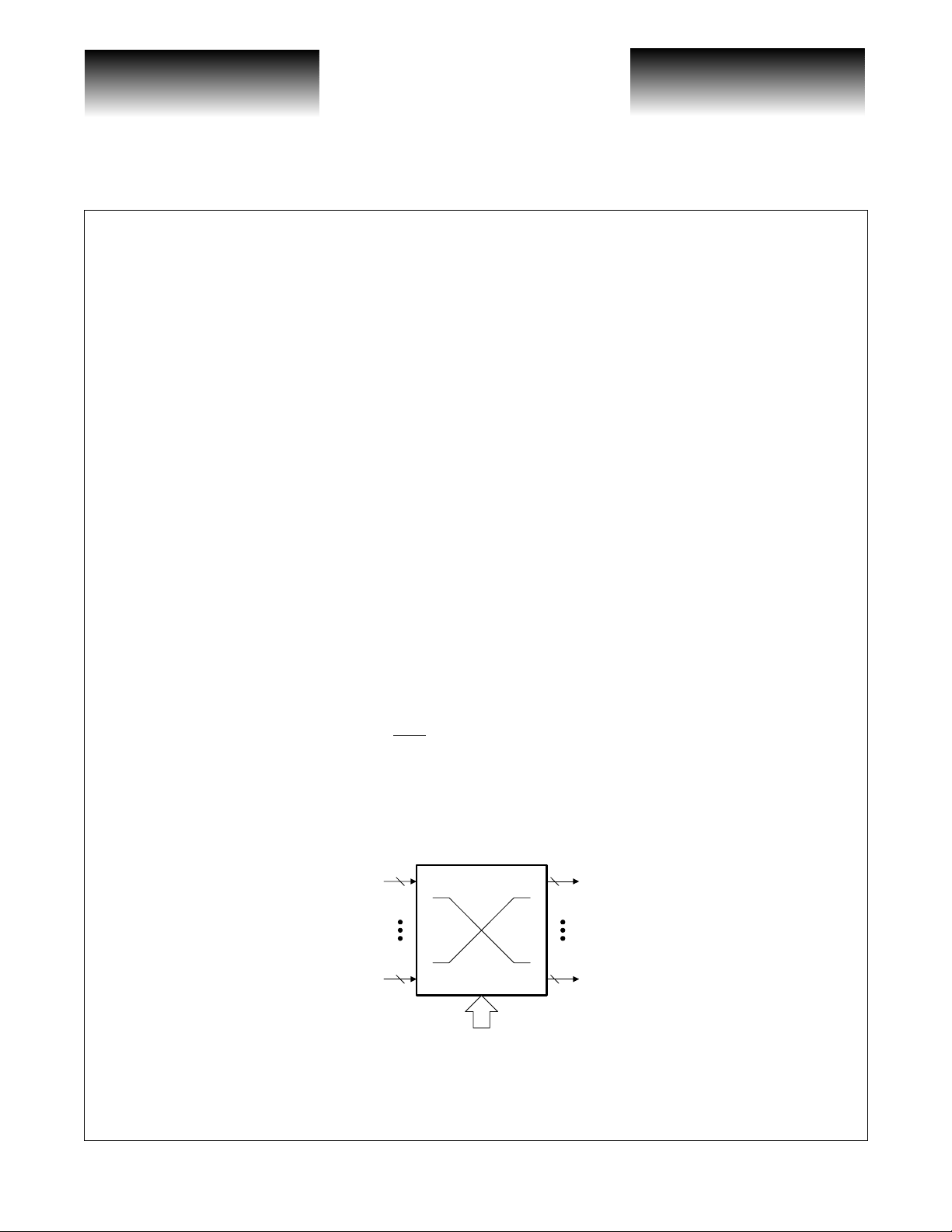
36x37 Crosspoint Switch
Features
• 36 Input by 37 Output Crosspoint Switch
• 3.2Gb/s NRZ Data Bandwidth
• Non-Blocking Architecture Broadcast and Multicast
Capabilities
• LVTTL/2.5V CMOS Control I/O (3.3V tolerant)
• Input Signal Activity Monitoring Function
• Integrated Signal Equalization (ISE) for Deterministic
Jitter Reduction
• 66MHz Dual Programming Port
• Parallel and Serial programming modes
• Programmable On-Chip I/O Termination
• Differential CML Output Drivers
• Single 2.5V Supply
• 6W Typical—Low Drive Mode
7W Typical—High Drive Mode
• High Performance 37.5mm, 480 TBGA Package
General Description
The VSC838 is a monolithic 36x36 asynchronous crosspoint switc h, designed to carry broadband data
streams. The VSC838 also has an interna l 37
Monitor to allow in system diagnostics.
A high degree of signal integrity is maintained throughout the chip via fully differential signal paths.
The crosspoint function is based on a multiplexer array architecture. Each data output is driven by a 36:1
multiplexer th at can be prog rammed to one and onl y o ne of its 36 inp uts. The s ignal path is u nregis tered and
fully asynchronous, so there are not any restrictions on the phase, frequency, or signal pattern at each input.
Each high-speed output is a fully differential, switched current driver with switchable on-die terminations
for maximum signal integ rity. Data inputs are terminated on-die th rough 100
complement inputs (see Input Termination section for further details).
A dual mode programming interface is provided that allows programming commands to be sent as serial
data or parallel data. Core programming can be random for each port address, or multiple program assignments
can be queued and issued simultaneously. The programming may be initialized to a “straight-through” configuration (A0 to Y0, A1 to Y1, etc.) using the INIT
Unused channels may be powered down to allow efficient use of the switch in appl ications that requi re only
a subset of the channels. Power-down can be accomplished in har dware, via ded icated power pins for pairs of
input and output channels, or in software by programming individual unused outputs with a disable code.
th
output channel which is used in conjunction with the Activity
Ω impedance between true and
pin.
3.2Gb/s
VSC838 Block Diagram
2 2
A0
2
A35
µ
P
control
G52351-0, Rev 3.0 Page 1
02/12/01
© VITESSE SEMICONDUCTOR CORPORATION • 741 Calle Plano • Camarillo, CA 93012
Tel: (800) VITESSE • FAX: (805) 987-5896 • Email: prodinfo@vitesse.com
Internet: www.vitesse.com
Y0
2
Y35
VITESSE
SEMICONDUCTOR CORPORATION
3.2Gb/s
36x37 Crosspoint Switch
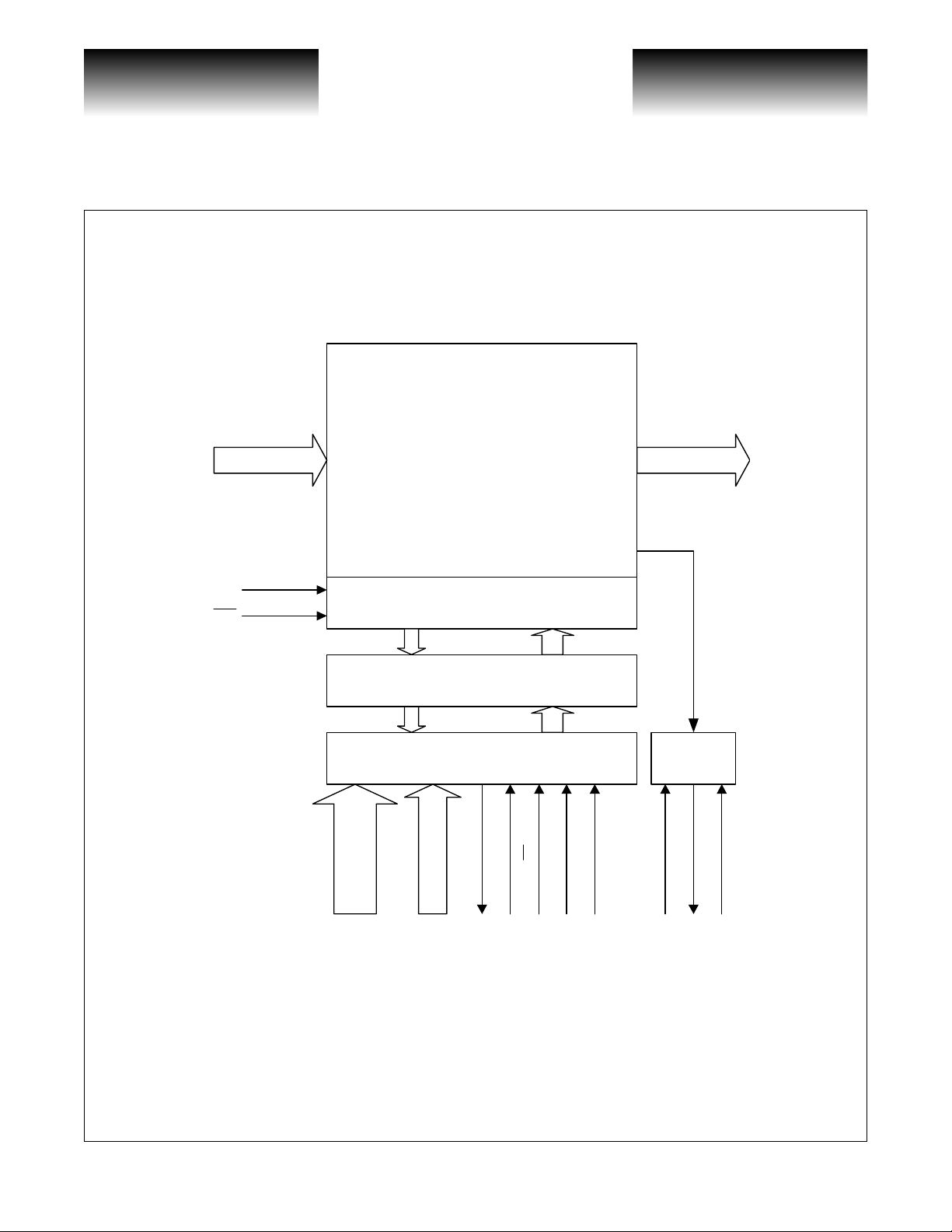
Functional Block Diagram
A, AN[0:35] Y, YN[0:35]
CONFIG
INIT
Preliminary Data Sheet
VSC838
36 x 37 SWITCH CORE
INTERNAL
37th OUTPUT
CORE PROGRAM REGISTERS
PROGRAM INTERFACE
OUTCHAN [5:0]
PROGRAM MEMORY
SDOUT
INCHAN [5:0]
SERIAL
CS
LOAD
ACTIVITY
MONITOR
ACTIVITY
ACTCHAN
ALE_SCN
ACTCLK
Page 2 G52351-0, Rev 3.0
© VITESSE SEMICONDUCTOR CORPORATION • 741 Calle Plano • Camarillo, CA 93012
Tel: (800) VITESSE • FAX: (805) 987-5896 • Email: prodinfo@vitesse.com
Internet: www.vitesse.com
02/12/01

VITESSE
SEMICONDUCTOR CORPORATION
Preliminary Data Sheet
VSC838
36x37 Crosspoint Switch
Functional Description
Input / Output Characteristics
All input data must be differential and should be nominally biased to +2.0V or AC-coupled. Other levels
are allowed as described under the Input Termination section. On-chip terminations are provided, with a nomi-
nal impedance of 100
coupling.
For direct interconnection of multiple VSC838 devices, a CML termination mode is provided by tying the
ITC pin to V
loads for an open-drain or open-collector differential output.
Data outputs are provided through differential current switches with on-chip back-termination. The output
circuit is capable of dri ving ex ternal 5 0
electronically switchable to enable a power savings of 1W (max) by reducing the output driver current.
CC
Ω differential. All input termination resistors float with an internal bias provided for AC-
, which ties the center point of the 100Ω termina tion to VCC, causing the terminat ions to act as
Ω far-end termination (recommended). The output back -terminatio ns are
Programming Interface
Parallel Mode
In parallel mode (SERIAL=0), the binary word on INCHAN[5:0] is the numerical identifier of the input
that will be routed to the specified output. OUTCHAN[5:0] is the numerical identifier of the output being programmed. A rising edge on the LOAD signal will transfer the p rogramming data to the shadow register in the
program memory. Raising CONFIG (asynchronously) will transfer the programming data to the main latches in
the program memory and cause the internal select signals in the core to re-configure the multiplexer. Lowering
CONFIG will latch the m ain la tches. C ONF IG may b e ti ed HI GH to ena ble p rog ram ming t o take effect insta ntaneously.
This interface may be used with multiplexed address/data buses by using only INCHAN[5:0] without
OUTCHAN[5:0] and dropping ALE when the address of the output to be programmed is present on
INCHAN[5:0]. After the address is latched, the input address may be presented on INCHAN [5:0] and programming proceeds as above.
No read-back capability is provided in parallel mode. Read-back for diagnostic purposes is provided in
serial mode via the scan function.
3.2Gb/s
Serial Mode
In serial mode (SERIAL=1), the INCHAN[0] pin becomes the serial data input SDIN and the INCHAN[1]
pin becomes the serial clock SCLK (rising edge triggered). A serial word of the form [Output][Input] is shifted
into the internal shift register, and the LOAD pin is asserted (HIGH) coincident with the last bit of the data word
to signal that the word is to be applied. This transfers the input identifier to the shadow register of the addressed
output. CONFIG is then applied ( asynchrono usly) to trans fer one or more prog ram comm ands to the main
latches of the program memories.
The SDOUT pin follows the data on the INCHAN[0](SDIN) pin 14 clock cycles later. This enables the user
to chain the serial ports of several crosspoints, shift program data for all switches through such a chain, and
assert LOAD on all switches simultaneously to program all of the connections simultaneously.
The output field is 7 bits long, representing the binary numerical identifier of the output to be programmed.
The input field is 7 bits long, representing the numerical identifier of the input that will be routed to the specified output.
G52351-0, Rev 3.0 Page 3
02/12/01
© VITESSE SEMICONDUCTOR CORPORATION • 741 Calle Plano • Camarillo, CA 93012
Tel: (800) VITESSE • FAX: (805) 987-5896 • Email: prodinfo@vitesse.com
Internet: www.vitesse.com

VITESSE
SEMICONDUCTOR CORPORATION
3.2Gb/s
Preliminary Data Sheet
36x37 Crosspoint Switch
Serial Read-Back
Read-back of the program memor y contents is acco mplished in serial m ode by s etting the ALE_SCN pin
HIGH. This will serially shift out the contents of the main latches in the program memories, slice 36 first and
slice 0 last, and MSB-first, LSB-last for each 7-bit word (see Figure 3). One rising edge of INCHAN[1](SCLK)
with ALE_SCN=0 and SERIAL=1 must occur to load the entire 483-bit shift register prior to shifting out data.
At a clock rate of 66MHz, this operation takes 7.26
Activity Monitoring
The activity monitor observes the output of the inte rnal 37th output from the core. By programming the
th
output to observe various inputs, the input signals can be scanned for activity or lack thereof. Each rising
37
edge of ACTCLK causes the monitor to read out the act ivity state from t he previous ACT CLK period and cl ears
the internal activity state until a data transition triggers it again. T here must be a min imum of one rising and one
falling edge on the observed input data pin during the ACTCLK period for activity to be detected. After poweron the output of ACTIVITY after the first ACTCLK rising edge is unknown.
To access the 37
th
output, ACTCHAN and INCHAN[5] must both be HIGH.
µs.
Selective Power-Down
Unused input and output channels can be made to consume little or no power via one of two methods of
selective power-down.
VSC838
Software Power-Down
Using this feature, unused outputs may be disabled, saving approximately 170 mW per channel for maximum dissipation conditions. This is accomplished by programming each unused output to look at input 127 (7F
Hex), which represents a non-existent input channel. The channel may be subsequently activated by programming a valid input address. It is recommended, however, that any changes in power programming only be executed as part of an initialization sequence to guard against the effects of any switching transients that might
result from changing the power supply current sudden ly. Software mode does not affect the functioning or
power of unused input channels.
Hardware Power-Down
Using this feature, the power associated with given pairs of inp uts may be shut of f by ty ing the corresponding V
tion conditions. The power associated with give n pairs of outputs, including their c ontribution to the core
power, can be shut off by tying the corresponding V
output pair is saved under the maximum dissipation conditions.
ing inputs and outputs will always be on and consuming power. See Figure 7 and Table 10 for the location of
these pins.
pin to VCC (see Table 10). Approximately 160 mW per input pai r is saved under the maximum dissipa-
EE
pin to VCC (see Table 10). Approximately 360 mW per
EE
Certain V
pins must always be active. In oth er words, t ied to t he most ne gative supp ly, so the correspond-
EE
Page 4 G52351-0, Rev 3.0
© VITESSE SEMICONDUCTOR CORPORATION • 741 Calle Plano • Camarillo, CA 93012
Tel: (800) VITESSE • FAX: (805) 987-5896 • Email: prodinfo@vitesse.com
Internet: www.vitesse.com
02/12/01
VITESSE
SEMICONDUCTOR CORPORATION
Preliminary Data Sheet
VSC838
36x37 Crosspoint Switch
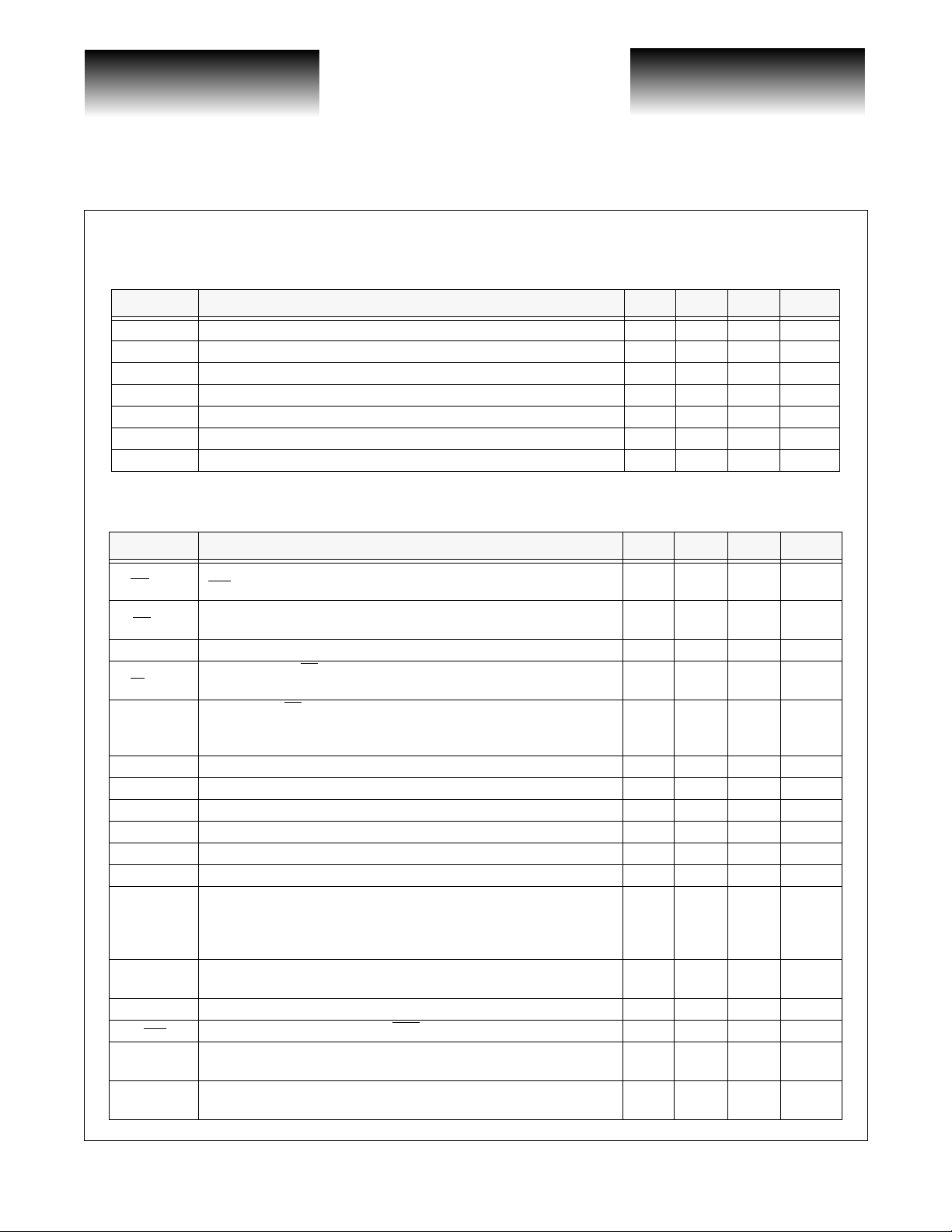
AC Characteristics
Table 1: Data Path
Parameter Description Min Typ Max Units
f
RATE
T
SKW
T
PDAY
, t
t
R
F
tR, t
F
t
jR
t
jP
NOTES: (1) Tested on a sample basi s onl y. (2) Broadband (unfiltered) determinis tic j it te r adde d to a jitter-free input, 223-1 PRBS data pattern.
T a ble 2: Program Interface Timing
Parameter Description Min Typ Max Units
T
sWR
T
hWR
T
PWLW
T
sCS
T
hCSB
T
PWCFG
T
sSDIN
T
hSDIN
T
perSCLK
T
sLOAD
T
hLOAD
T
sSERIAL
T
hSERIAL
T
dSDOUT
T
PWINIT
T
sSCAN
T
hSCAN
Maximum data rate - - 3.2 Gb/s
Channel-to-channel delay skew - 300 - ps
Propagation Delay from an A input to a Y output - 750 - ps
High-speed input rise/fall times, 20% to 80% - - 150 ps
High-speed output rise/fall times, 20% to 80% - - 150 ps
Output added delay jitter, rms
Output added delay jitter, peak-to-peak
Setup time from INCHAN[5:0] or OUTCHAN5:0] to rising edge of
.
WR
Hold time from rising edge of WRB to INCHAN[5:0] or
OUTCHAN[5:0].
Pulse width (HIGH or LOW ) on LOAD 6.75 —— ns
Setup time from CS to falling edge of LOAD or ALE_SCN in parallel or
burst mode, or rising edge of LOAD in serial mode.
Hold time of CS rising edge after LOAD or ALE_SCN rising in parallel
or burst mode, or falling edge of LOAD in serial mode, or falling edge of
CONFIG in any mode.
Pulse width (HIGH or LOW) on CONFIG. 6.75 —— ns
Setup time from INCHAN0(SDIN) to INCHAN1(SCLK) rising. 1.65 —— ns
Hold time of INCHAN0(SDIN) after INCHAN1(SCLK) rising. 1.0 —— ns
Minimum period of SCLK in serial mode. 15 —— ns
Setup time from LOAD to INCHAN1(SCLK) rising. 1.85 —— ns
Hold time of LOAD after INCHAN1(SCLK) rising. 0.95 —— ns
Setup time from SERIAL rising to INCHAN1(SCLK) rising when
entering serial mode or SERIAL falling to LOAD falling when entering
parallel mode or SERIAL falling to LOAD rising when entering burst
mode.
Hold time from INCHAN1(SCLK) rising to SERIAL falling when
exiting serial mode.
Delay from INCHAN1(SCLK) rising to SDOUT, 20pF load. ——6.20 ns
Pulse width (HIGH or LOW) on INIT.6.75—— ns
Setup time from ALE_SCN to INCHAN1(SCLK) rising when starting
or completing a serial read-back sequ ence.
Hold time of ALE_SCN after INCHAN1(SCLK) rising when starting or
completing a serial read-back sequence.
(1, 2)
(1, 2)
-10ps
-40ps
3.35 —— ns
1.45 —— ns
0 —— ns
0 —— ns
0.90 —— ns
0 —— ns
1.65 —— ns
1.0 —— ns
3.2Gb/s
G52351-0, Rev 3.0 Page 5
02/12/01
© VITESSE SEMICONDUCTOR CORPORATION • 741 Calle Plano • Camarillo, CA 93012
Tel: (800) VITESSE • FAX: (805) 987-5896 • Email: prodinfo@vitesse.com
Internet: www.vitesse.com
VITESSE
SEMICONDUCTOR CORPORATION
3.2Gb/s
36x37 Crosspoint Switch
Figure 1: Parallel Mode -- Separate Address/Data (leave ALE_SCN pin HIGH)
OUTCHAN[5:0]
INCHAN[5:0]
LOAD
CONFIG
SERIAL
INCHAN[5:0]
Output Addr
Input Addr
T
T
sWR
CS
T
T
Figure 2: Parallel Mode -- Multiplexed Address/Data
sCS
PWLW
T
sSERIAL
hWR
Output Addr Input Addr
Preliminary Data Sheet
VSC838
T
hCS
T
PWCFG
ALE_SCN
LOAD
CS
CONFIG
SERIAL
T
hCS
T
T
sWR
hWR
T
sCS
T
sSERIAL
T
PWLW
T
PWCFG
Page 6 G52351-0, Rev 3.0
© VITESSE SEMICONDUCTOR CORPORATION • 741 Calle Plano • Camarillo, CA 93012
Tel: (800) VITESSE • FAX: (805) 987-5896 • Email: prodinfo@vitesse.com
Internet: www.vitesse.com
02/12/01
 Loading...