

VITESSE VSC835UB Datasheet
VITESSE SEMICONDUCTOR CORPORATION
Page 1
7/24/00 741 Calle Plano, Camarillo, CA 93012 • 805/388-3700 • FAX: 805/987-5896
VITESSE
SEMICONDUCTOR CORPORATION
Datasheet
SC835
2.5 Gbits/sec
34x34 Crosspoint Switch with Signal Detection
G52270-0, Rev. 4.1
Features
General Description
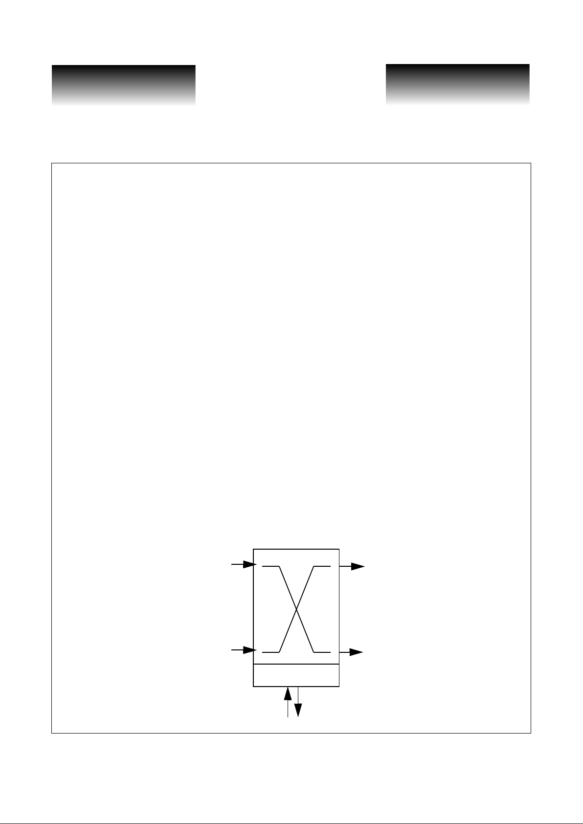
The VSC835 is a monolithic 34x34 asynchronous crosspoint sw itch, designed to carry broadband data
streams at up to 2.5 Gbit/s. The non-blocking switch core is programmed through a parallel port interface that
allows random access programming of each outpu t port. A high degree of signal integrity is maintained through
the chip through fully differential signal paths.
The crosspoint func tion is based o n a multip lexer tree archit ecture. Eac h data outp ut is drive n by a 34:1
multiplexer tree that can be programmed to one and only one of its 34 inputs, and each data input can be routed
to multiple outputs. The signa l path is unr egist ered, so n o clock i s requi red for the dat a input s. The sign al path is
asynchronous, so there are no r estrictions on the phase, frequenc y, or signal pattern at each input. Each input
channel and each output channel has an signal monitor function that can be used to identify loss of activity
(LOA). An interrupt pin is provided to signal LOA, after whi ch an external controller can query the chip to
determine the channel(s) on which the fault occurred.
Each output driver is a fully differential switched current driver with on-die back-terminations for maximum signal integrity. Data inputs are terminated on die through 50 ohm resistors terminated to V
TERM
.
The parallel interface uses TTL levels, and provides address, data, and control pins that are compatible
with a microprocessor-style interface . The control port provi des access to all chip functio ns, includin g LOA and
programming. Program buffering is provided to allow multiple program assignments to be qu eued and issued
simultaneously via a single configure command.
VSC835 Block Diagram
• 34 Input by 34 Output Crosspoint Switch
• 2.5 Gbits/sec. NRZ Data Bandwidth
• TTL Compatible µP Interface
• Differential PECL Data Inputs
• On-chip 50Ω Input Terminations
• 50Ω Source Terminated PECL Output Drivers
• Single 3.3V Supply
• 14W Maximum Power Dissipation
• High Performance 256 BGA Package
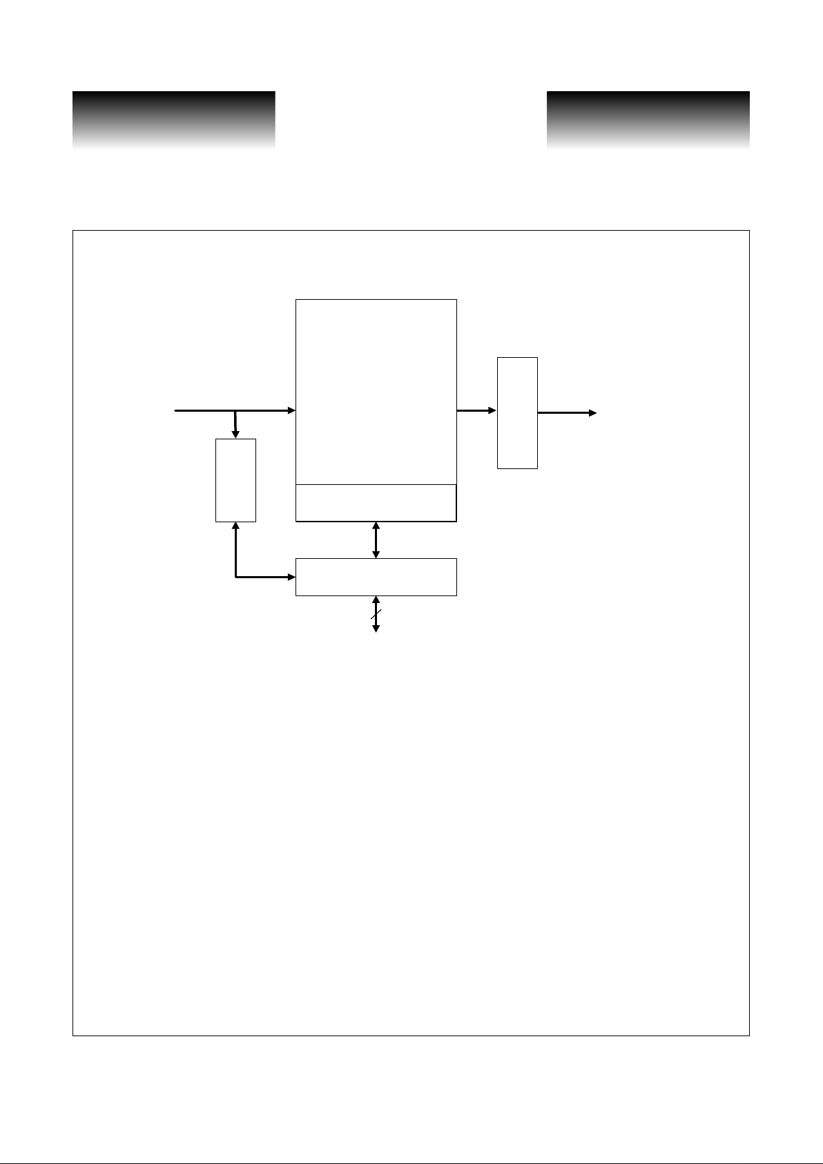
Control Logic
µP interface
A0
Y0
A33
Y33
VITESSE
SEMICONDUCTOR CORPORATION
Datasheet
VSC835
2.5 Gbits/sec
34x34 Crosspoint Switch with Signal Detection
Page 2
VITESSE SEMICONDUCTOR CORPORATION
741 Calle Plano, Camarillo, CA 93012 • 805/388-3700 • FAX: 805/987-5896 7/24/00
G52270-0, Rev. 4.1
Figure 1: Detailed Block Diagram
Functional Description
Data Paths
All input data must be differential and biased to PECL levels. On-ch ip terminations are pro vided, with a
nominal impedance of 50 ohms. All input termination resistors are tied to V
TERM
.
Data outputs are provided throug h differential current switc hes with on-chip te rminations that produce a
PECL level output swing. The drive level of the output circuit is designed to produce standard PECL levels
when terminated in 50 ohms to 2.0 volts. Other termination voltages are possible, such as to VCC or 1.3 volts,
but the voltage level of t he ou tp ut wil l be shi f te d f rom it s no min a l v alu e. T he commo n- mode v olt ag e of the output swing can be adjusted using t he VCOM pins. The adjustment range is n ot cal ibrate d, but t ypicall y all ows for
+/- 200mV of adjustment in common-mode voltage. The VCOM pin self-biase s to a nominal value when left
unconnected.
Output channels can be powered off in pairs if fewer than 34 outputs are required. By connecting the VEE
pin associated with a given pair of outputs to VCC, the output pairs will pull to VCC and chip power will be
reduced by approximately 300mW per pair.
A,AN[33:0]
Control interface
DATA[5:0], ADDR[5: 0]
ALE, CSB, WRB, RDB
INTB, MONCLK, CONFIG
Y,YN[33:0]
34
LOA
monitor
34 x 34
switch core
Program memory
output drivers
VITESSE SEMICONDUCTOR CORPORATION
Page 3
7/24/00 741 Calle Plano, Camarillo, CA 93012 • 805/388-3700 • FAX: 805/987-5896
VITESSE
SEMICONDUCTOR CORPORATION
Datasheet
SC835
2.5 Gbits/sec
34x34 Crosspoint Switch with Signal Detection
G52270-0, Rev. 4.1
Programming Interface
The switch core is programmed through a pa ra llel i nterface ci rcuit t hat al lo ws ra ndom reads or wri tes t o t he
program memory array. The program memory array is buffered to allow multiple programming instructions to
be loaded simultaneously with the CONFIG pin. Parallel programing can be clocked at up to a 50MHz rate and
state read-back can be performed at up to 25MHz.
The program data is composed of two parts: output address and input address. The output address, denoted
by ADDR[5:0], specifies which outpu t chann el is to be programmed. Th e input ad dress, denot ed by DAT A[5: 0],
specifies which input port the switch slice should connect to. The format of the program data is simple binary.
For example: ADDR[5:0] (000100) / DATA[5:0] (000110) would direct output channel Y4 to connect to input
channel A6. The programming state may be verified (read back) by applying the address of the desired output
and asserting RDB. The programming state is unknown at power-on. Additional address space is provided for
access to the monitor registers (see sections below). The microprocessor interface consists of the following signals. Levels are TTL (see DC Characteristics)
:
Loss of Activity (LOA) Monitoring
The LOA function consists o f an activity monitor on each input c hannel, co nnected dire ctly to the p ads.
The state of a monitor (whether or not it has been toggled by an input transition) can be observed by applying
the address
1
of the monitor register correspondin g to the signal of int erest and asserting RDB . Each monitor
register is four bits in length, covering the state of four inputs. There is on e extra two-bit monitor for the 33
rd
and 34th inputs. The state of each monitor is transferred to the register on the rising edge of MONCLK, whereupon the activity monitor is cleared until more activity is detected.
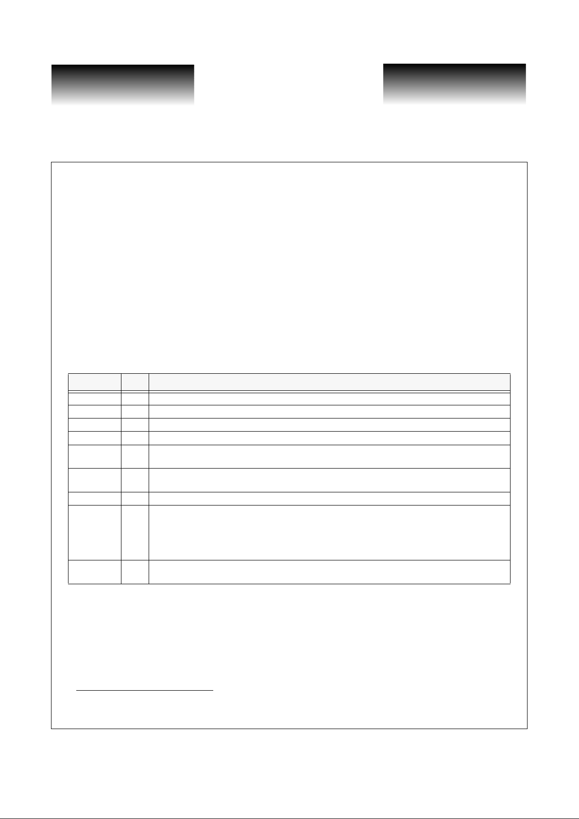
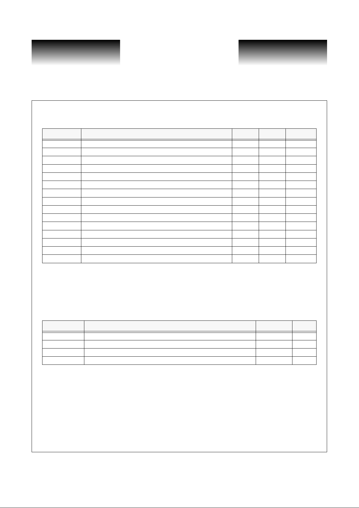
Table 1: Programming Interface Signal Table
Pin I/O Description
D[5:0] B Bidirectional data bus to transfer data to/from internal program registers
A[5:0] I Address bus to select internal program registers for read-write operations
ALE I ALE functionality is not implemented at this time. Tie this pin High.
CSB I Chip Select (Active Low): assert this pin whenever the part is being read or programmed.
WRB I
Write (Active Low): program data will be transferred to the first level internal registers on the rising
edge of this signal (when CSB is also low).
RDB I
Read (Active Low): program data from the internal program or moni tor registers will be read out on the
data bus when this signal goes low (with CSB also low).
INTB O Interrupt (Active Low): this signal is asserted when an LOA condition is found
CONFIG I
Configure (Active High): assert this signal to transfer queued program infor matio n from the first-leve l
internal registers to the second-level registers, making the programming take effect. This signal may be
tied high to leave the second-level registers transparent so all programming will take effect
immediately. CSB must be active (low) when CONFIG is asserted. CONFIG may be tied to a highorder bit of the address bus
MONCLK I
Monitor states are tr ansferred to monitor registers on the ri sing edge of this signal. MONCLK is not
expected to exceed 3MHz.
1. See Memory Map Table
VITESSE
SEMICONDUCTOR CORPORATION
Datasheet
VSC835
2.5 Gbits/sec
34x34 Crosspoint Switch with Signal Detection
Page 4
VITESSE SEMICONDUCTOR CORPORATION
741 Calle Plano, Camarillo, CA 93012 • 805/388-3700 • FAX: 805/987-5896 7/24/00
G52270-0, Rev. 4.1
If any change in a monitor state occurs after samplin g by MONCLK, an interrupt will be signalled by
asserting INTB, and the user must identify the offending channel by reading the monitor states . The interrupt
will be cleared when the corresponding activity monitor is read, bu t the monitor state will not be changed. If
multiple monitors have triggered the interrupt, it will persist until all the corresponding monitors have been
read.
LOA requires a minimum signal level of 30-150m V peak-peak to recognize an input as active. This is
required to distinguish noise on an unconnected signal (where both inputs float to the termination voltage) from
activity on a live sign al. A mi ni mum of t wo tra nsiti ons d efine s ac tivit y. The threshold signal le vel is c on trolle d
by the voltage on the VHYS pin. In order to keep the hysteresis in a useful range, it is recommended that VHYS
be nominally tied to VCC (useful range is 2.0V t o VCC ).
.
AC Characteristics
note: Unless otherwise stated, all specifications are guaranteed but not tested.
note 1: Skew between any two input channels to a given output.
note 2: Skew between any two output chann els from the same input channel.
note 3: Required for high-speed output rise/fall spec at F
RATE
=2.5 Gbits/s. For lower rate signals, use 0.375/F
RATE
note 4: Broadband jitter added to a jitter-free signal; jitter is primarily in the form of ISI for random data
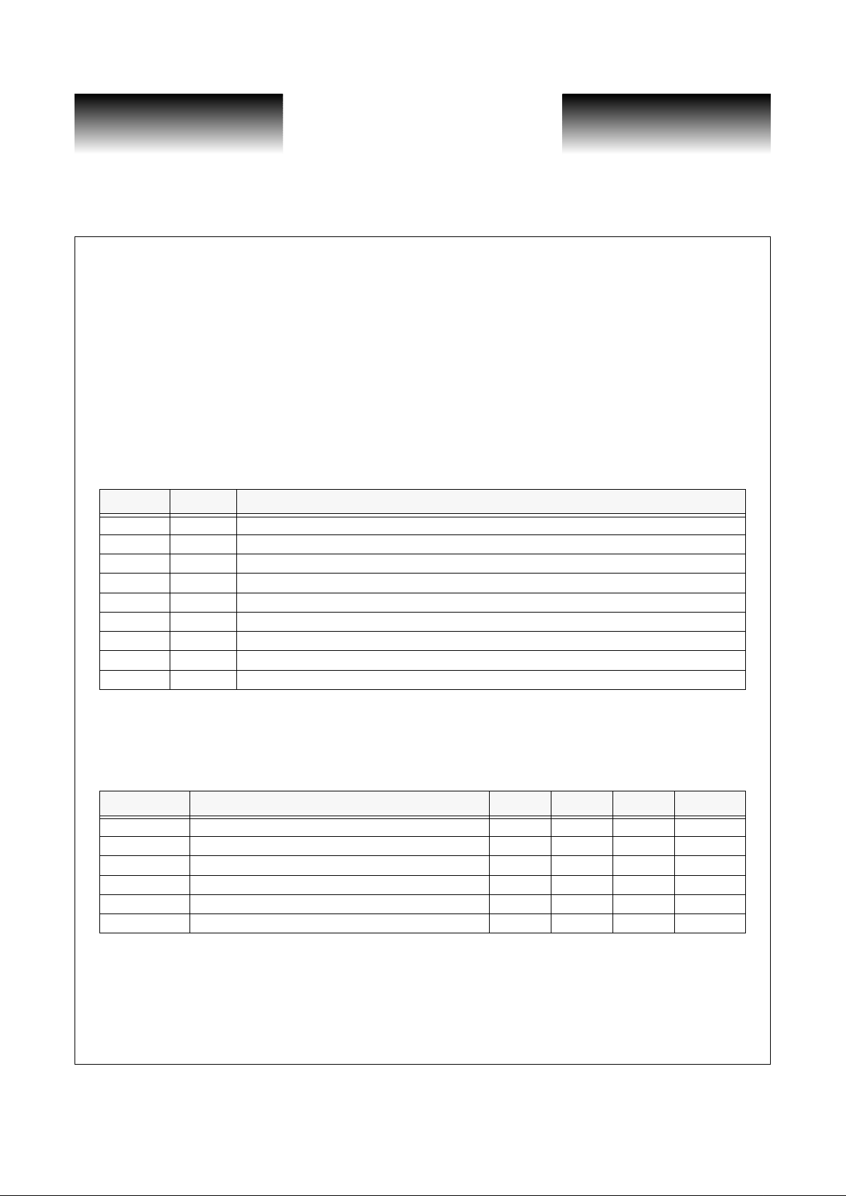
Table 2: Memory Map
Address Access Description
00h R/W Output Y0’s programmed input channel (write and then assert CONFIG to program)
01h R/W Output Y1’s programmed input channel
... ... ...
21h R/W Output Y33’s programmed input channel
22h, 23h R/O Rx Signal monitor for inputs [A0-A3], [A4-A7] (Logic ‘1’=No activity)
24h, 25h R/O Rx Signal monitor for inputs [A8-A11], [A12-A15]
26h, 27h R/O Rx Signal monitor for inputs [A16-A19], [A20-A23]
28h, 29h R/O Rx Signal monitor for inputs [A24-A27], [A28-A31]
2Ah R/O Rx Signal monitor for inputs [A32-A33]
Table 3: Data Path
Parameter Description Min Typ Max Units
F
RATE
Data rate - - 2.5 Gbits/s
T
ISKW
Input channel de lay skew (1) - 300 - ps
T
OSKW
Output channel delay skew (2) - 300 - ps
tR, t
F
High-speed input rise/fall times, 20% to 80% (3) - - 150 ps
tR, t
F
High-speed output rise/fall times, 20% to 80% - - 150 ps
t
jP
Output data eye jitter, peak-peak, 2
31
PRBS (4) - - 100 ps
VITESSE SEMICONDUCTOR CORPORATION
Page 5
7/24/00 741 Calle Plano, Camarillo, CA 93012 • 805/388-3700 • FAX: 805/987-5896
VITESSE
SEMICONDUCTOR CORPORATION
Datasheet
SC835
2.5 Gbits/sec
34x34 Crosspoint Switch with Signal Detection
G52270-0, Rev. 4.1
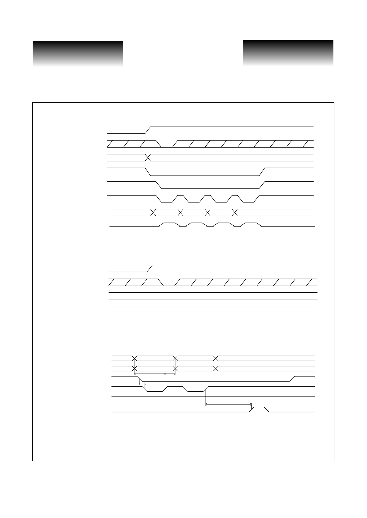
Figure 2: Figure 2: Interrupt Timing (Change in Monitor State Registers)
Figure 3: Figure 3: Interrupt Timing (No change in Monitor State Registers)
Figure 4: Figure 4: Program Timing
MONCLK
Monitor State
Monitor State Reg
INTB
MONCLK
Monitor State
Monitor State Reg
INTB
ADR[5:0]
D[5:0]
CSB
WRB
RDB
CONFIG
T
sCSB
T
sWRB
T
hWRB
T
sCONFIG
VITESSE
SEMICONDUCTOR CORPORATION
Datasheet
VSC835
2.5 Gbits/sec
34x34 Crosspoint Switch with Signal Detection
Page 6
VITESSE SEMICONDUCTOR CORPORATION
741 Calle Plano, Camarillo, CA 93012 • 805/388-3700 • FAX: 805/987-5896 7/24/00
G52270-0, Rev. 4.1
note 1: measured from falling edge.
note 2: measured from rising edge.
DC Characteristics
(over the specified operating conditions)
Note: Icc Specified with outputs terminated with 50 ohms to +2.0V and Chip Vterm=+2.0V, Vcc = 3.45V
Table 4: Programming Port Interface Timing
Parameter Description Min Max Units
T
config
Switch configuration delay - 6 ns
T
pdADDR
Data read propagation delay from ADDR - 30 ns
T
pdRDB
Data read propagation delay from RDB (1) - 7 ns
T
pdint
Interrupt propagation delay from MONCLK (2) - 50 ns
T
pdstate
MONCLK to internal state register change delay (2) - 6 ns
T
sRDB
ADDR to RDB setup time 5 - ns
T
hRDB
RDB to ADDR hold time 3 - ns
T
sWRB
WRB setup time (for either ADDR or DATA) 5 - ns
T
hWRB
WRB hold time (for either ADDR or DATA) 3 - ns
T
sCONFIG
WRB to CONFIG setup time 1 - ns
T
sCSB
CSB setup time (to either WRB or RDB) 0 - ns
T
pwCONFIG
CONFIG pulse width (high) 10 - ns
T
pwWRB
WRB pulse width (low and high) 10 - ns
T
pwRDB
RDB pulse width (low and high) 10 - ns
T
tsDATA
DATA tri-state delay (from either RDB or CSB) (2) - 10 ns
Table 5: Powe r
Parameter Description (Max) Units
I
CC
VCC supply current 4060 mA
P
T
Total chip power 14 W
I
TERM-V
V
TERM
supply current with V
TERM =VCC
-1.3V ~0 mA
I
TERM-E
V
TERM
supply current with V
TERM =VCC
-2.0V -950 mA
 Loading...