

VITESSE VSC830QZ Datasheet
VITESSE
SEMICONDUCTOR CORPORATION
Data Sheet
VSC830
2.7Gb/s Asynchronous
Dual 2x2 Crosspoint Switch
Features
• Dual 2x2 Crosspoint Switch
• 2.7Gb/s NRZ Data Bandwidth, 2.7GHz Signal
Bandwidth
• PECL/TTL-Compatible Control Inputs
• PECL-Compatible High-Speed I/O
• 50
Ω Source Terminated Output Driver and
Programmable Input Terminations
• Single 3.3V Supply, 1W Typical Dissipation
• Power-Down Capability for Unused Outputs
• Compact 44-Pin PQFP, 10x10mm Package
General Description
The VSC830 is a monolithic dual 2x2 asynchronous crosspoint switch, designed for critical signal path
control and buffering applications, such as loop-back, protection switching, and multi-channel backplane
driver/receivers. Signal path delay is tightly matched between each output channel to eliminate the need for
delay path compensation when switching between signal sources.
The crosspoint function is based on a multiplexer tree architecture. Each 2x2 switch can be considered as a
pair of 2:1 multiplexers that share the same inputs. The signal path through each switch is fully differential and
delay matched. The signal path is u nregistered, s o there are no restrictions on the phase, fre quency, or signal
pattern at each input. Unused outputs can be independently powered off, thereby eliminating power on unused
sections (see Design Guide section in this data sheet). The switch control inputs can be configured to be compatible with PECL or TTL levels. The high-speed input and output levels are nominally PECL compatible and
capable of interfacing with a wide range of termination schemes.
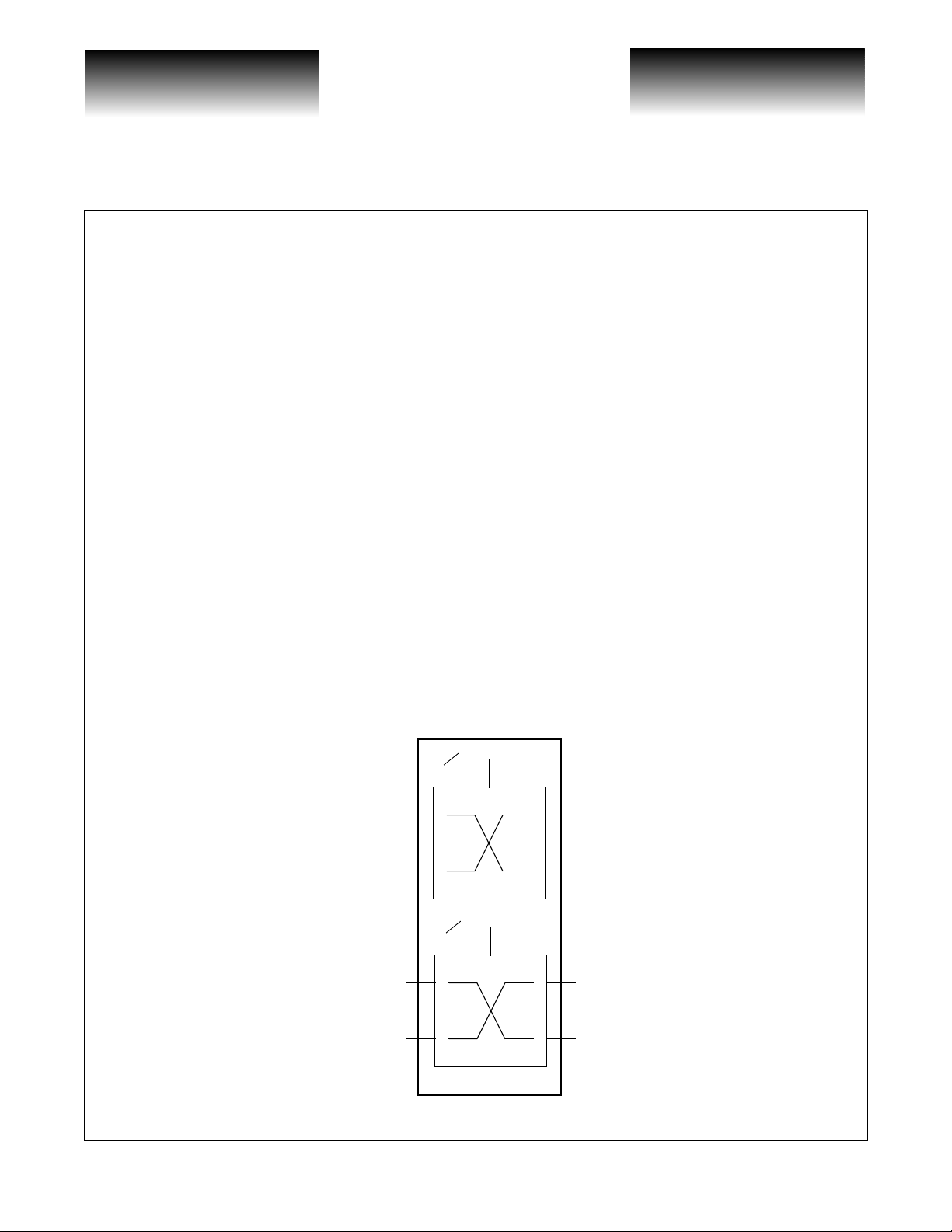
VSC830 Symbol Diagram
S1,S2
S1,S2
A1
Y1
A2 Y2
A1
Y1
A2 Y2
G52192-0, Rev 4.0 Page 1
05/23/01
© VITESSE SEMICONDUCTOR CORPORATION • 741 Calle Plano • Camarillo, CA 93012
Tel: (800) VITESSE • FAX: (805) 987-5896 • Email: prodinfo@vitesse.com
Internet: www.vitesse.com
VITESSE
SEMICONDUCTOR CORPORATION
2.7Gb/s Asynchronous
2.7Gb/s Asynchronous
Dual 2x2 Crosspoint Switch
Functional Block Diagram
PEMODE VCC
S1A
A1A+
A1A-
TERM_ENABLE_A
S2A
A2A+
Data Sheet
VSC830
VCCP1A
SL
0
1
SL
0
Y1A
Y1AN
VEE1A
VCCP2A
Y2A
A2A-
S1B
A1B+
A1B-
TERM_ENABLE_B
S2B
A2B+
A2B-
1
SL
0
1
SL
0
1
Y2AN
VEE2A
VCCP1B
Y1B
Y1BN
VEE1B
VCCP2B
Y2B
Y2BN
VEE2B
Page 2 G52192-0, Rev 4.0
© VITESSE SEMICONDUCTOR CORPORATION • 741 Ca l le Pl an o • Camarillo, CA 93012
Tel: (800) VITESSE • FAX: (805) 987-5896 • Email: prodinfo@vitesse.com
Internet: www.vitesse.com
05/23/01
VITESSE
SEMICONDUCTOR CORPORATION
Data Sheet
VSC830
2.7Gb/s Asynchronous
Dual 2x2 Crosspoint Switch
Functional Description
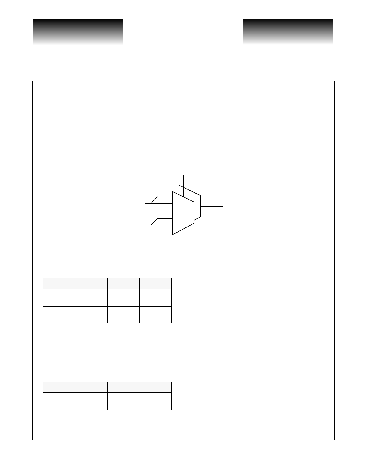
Select
As shown in Figure 1, each output can be treated as a 2:1 multiplexer, with the A1 and A2 inputs common
to both multiplexers. The select input S1 independently controls the state of the multiplexer that drives output
Y1, and select input S2 independently controls the output of Y2.
Figure 1: Select Functional Block Diagram
S1
S2
A1
A2
Y1
Y2
Table 1 specifies the function of the select inputs.
Table 1: Select Function
S1 S2 Y1 Y2
0 0 A1 A1
1 0 A2 A1
0 1 A1 A2
1 1 A2 A2
MODE
The interface level of the select pins, S 1 and S2, can be prog rammed to either T TL or PECL levels by shorting the MODE pin to either V
tion of MODE is specified in Table 2.
Table 2: MODE Function
MODE S1, S2
V
EE
V
CC
or VEE. Note that the MODE pin must be ti ed to ei ther VCC or VEE. The func-
CC
TTL
PECL
G52192-0, Rev 4.0 Page 3
05/23/01
© VITESSE SEMICONDUCTOR CORPORATION • 741 Calle Plano • Camarillo, CA 93012
Tel: (800) VITESSE • FAX: (805) 987-5896 • Email: prodinfo@vitesse.com
Internet: www.vitesse.com
VITESSE
SEMICONDUCTOR CORPORATION
2.7Gb/s Asynchronous
2.7Gb/s Asynchronous
Dual 2x2 Crosspoint Switch
Power-Down
Power to each output s tage is provided through VCC, V
power off unused outputs, tie the respective V
Figure 2: Power-Down Mode Example
V
CC
V
1A
CCP
V
1A
EE
“ON”
“ON”
Data Sheet
VSC830
, and VEE. VCC is comm on to all ou tpu ts . To
CCP
and V
EE
V
2A
CCP
V
2A
EE
pin to VCC, as shown in Figure 2.
CCP
V
1B
CCP
V
“OFF”
EE
1B
V
“OFF”
V
EE
CCP
2B
2B
Minimum power configuratio n requires outp ut channel 1A active, so power must be applied to V
and V
Programmable input termination
tion resistor. Using the TERM_ENABLE pin, the termination can be optionally disabled. To enable the input
termination, connect the respective TERM_ENABLE pin to V
TERM_ENABLE to V
nal termination. Independent termination controls are provided for the “A” and “B” switches.
1A at all times.
EE
Across each differential input (from the + input to the - input) of the VSC830 is a switched 100Ω termina-
. To disable the internal termination, connect
CC
. If unconnected, the TERM_ENAB LE pi n will se lf- bi as t o VEE and disable the inter-
EE
CCP
1A
Page 4 G52192-0, Rev 4.0
© VITESSE SEMICONDUCTOR CORPORATION • 741 Ca l le Pl an o • Camarillo, CA 93012
Tel: (800) VITESSE • FAX: (805) 987-5896 • Email: prodinfo@vitesse.com
Internet: www.vitesse.com
05/23/01
VITESSE
SEMICONDUCTOR CORPORATION
Data Sheet
VSC830
2.7Gb/s Asynchronous
Dual 2x2 Crosspoint Switch
AC Characteristics
Table 3: AC Timing
Symbol Parameter Min Typ Max Units
F
RATE
F
BW
T
SKW
T
CON
, t
t
R
F
t
jP
NOTES: (1) Tested on a sample basis only, with 223-1 PRBS data, input signal rise/fall ti me < 150p s. Value stated i n table is add ed
to measurement system jitter. (2) Input signal rise/fall time < 150ps, measured using an alternating 1, 0 pattern.
Signal path data ra te 2.7 Gb/s
Signal path bandwidth (-3dB) 2.7 GHz
Channel to channel delay skew 50 ps
Switch configur ation setup time
High-speed output rise/fall times, 20% to 80%
Signal path added jitter, peak-peak
(1)
(1)
(2)
1ns
150 ps
40 ps
DC Characteristics (All characteristics are over the specified operating conditions)
Table 4: Power Supply
Symbol Parameter Min Typ Max Units Conditions
I
CC
P
D
P
T
NOTE: Specified with outputs terminated, 100Ω between true and c omplement, VCC = 3.45V.
Table 5: Select Input Levels—TTL Mode
Total V
Power dissipation per output
(Y1A±, Y2A±, Y1B±, Y2B±)
Total chip power (all outputs powered on) 1.2 W
supply current 350 mA
CC(P)
300 mW
Symbol Parameter Min Typ Max Units Conditions
V
IH
V
IL
I
IH
I
IL
Input HIGH voltage (TTL) 2.0 V
Input LOW voltage (TTL) 0.8 V
Input HIGH current (TTL) 500 µAVIN = 2.4V
Input LOW current (TTL) -500 µAVIN = 0.5V
Table 6: Select Input Levels—PECL Mode
Symbol Parameter Min Typ Max Units Conditions
-
V
V
IH
V
IL
I
IH
I
IL
Input HIGH voltage (PECL)
Input LOW voltage (PECL)
Input HIGH current (PECL) 500 µAVIN = 2.5V
Input LOW current (PECL) -500 µAVIN = 1.5V
CC
1.0
V
-
V
CC
1.6
V
Table 7: Control Inputs
Symbol Parameter Min Typ Max Units Conditions
R
PEMODE
G52192-0, Rev 4.0 Page 5
05/23/01
PEMODE pin im pedance 3100 Ω
© VITESSE SEMICONDUCTOR CORPORATION • 741 Calle Plano • Camarillo, CA 93012
Tel: (800) VITESSE • FAX: (805) 987-5896 • Email: prodinfo@vitesse.com
Internet: www.vitesse.com
VITESSE
SEMICONDUCTOR CORPORATION
2.7Gb/s Asynchronous
Data Sheet
2.7Gb/s Asynchronous
Dual 2x2 Crosspoint Switch
Table 8: “A” Input Levels (Differential PECL)
Symbol Parameter Min Typ Max Units Conditions
V
ID
V
ICM
NOTE: (1) Peak-to-peak swing of each side of the differential input.
Input differential voltage 200 1000 mV See Note 1
Input common-mode voltage
-
V
CC
1.7
VCC-
0.9
V
Table 9: “Y” Output Levels (Differential PECL)
Symbol Parameter Min Typ Max Units Conditions
V
OD1
V
OD2
V
OCM
NOTES: (1) Peak-peak swing of each side of the differential output. 223-1 PRBS data. (2) Peak-to-peak sw ing of each side of the
Output differential voltage (Data) 400 700 1000 mV See Note 1
Output differential voltage (Clock) 400 550 850 mV See Note 2
Output common-mod e voltage
differential output. Alternating 1, 0 pattern.
-
V
CC
1.6
VCC-
1.0
V
VSC830
Absolute Maximum Ratings
Power Supply Voltage (VCC) Potential to GND ..............................................................................-0.5V to +4.0V
TTL Input Voltage Applied ...................................................................................................-0.5V to V
ECL Input Voltage Applied ....................................................................................................-0.5V to V
Output Current (I
Case Temperature Under Bias (T
Storage Temperature (T
NOTE: (1) Caution: Stresses listed under “Ab solu te M axi mum R ati ngs” may be appl ied to dev ices one a t a t ime wi th out causi ng
permanent damage. Functionality at or exceeding the values listed is n ot implied. Exposure to these values for extended
periods may affect device reliability.
) ....................................................................................................................................50mA
OUT
) .............................................................................................-55oC to + 125oC
C
)........................................................................................................-65oC to + 150oC
STG
CC
CC
+0.5V
+0.5V
Operating Conditions
Supply voltage (VEE) ..........................................................................................................................................0V
Supply voltage (V
Supply voltage (V
Operating Range
NOTE: (1) Lower limit of specification is ambient temperature and upper limit is case temperature.
)............................................................................................................................+3.3V ±5%
CC
) .......................................................................................................................... +3.3V ±5%
CCP
(1)
(T) ..................................................................................................................... 0oC to +85oC
ESD Ratings
Proper ESD procedures should be used when handling this product. The VSC830 is rated to the following
ESD voltages based on the human body model:
1. All pins are rated at or above 1500V.
Page 6 G52192-0, Rev 4.0
© VITESSE SEMICONDUCTOR CORPORATION • 741 Ca l le Pl an o • Camarillo, CA 93012
Tel: (800) VITESSE • FAX: (805) 987-5896 • Email: prodinfo@vitesse.com
Internet: www.vitesse.com
05/23/01
 Loading...