

VITESSE VSC8185 Datasheet
www.vitesse.com
Product Brief
11.5-12.5Gb/s 16:1 Multiplexer with Clock Generator
Physical
Layer
Products
Physical Layer Products
VSC8185
General Description
The VSC8185 consists of a 16:1 Multiplexer and a clock generator for use
in SONET STS-192 / SDH STM-64
systems. The 16:1 Multiplexer accepts
16 parallel low voltage differential
swing (LVDS) inputs (D[0:15]±) and
(PARITY±) at a data rate of 718.8 to
781.3 Mb/s. This parallel data stream
is then serialized into a 11.5Gb/s to
12.5Gb/s output (DOUT±). The clock
generator creates the 11.5GHz to
12.5GHz clock signal used to re-time
the transmitted serialized data. The
clock generator requires a 180195MHz or 719-781MHz PECL reference clock input (REFCK±). To ease
timing constraints on the parallel interface, a 16 bit wide FIFO is included. A
high speed clock output (COUT±) is
provided that is synchronized to the
high speed serial data output. A divideby-16 or divide-by-64 LVDS clock output (CK16_64±) is available for use as
a clock input to the data source of the
parallel inputs (D[0:15]±) and (PARITY±). Additional features include parity bit (P ARITY±) that is clocked in with
the 16-bit parallel data. Bit Order Swap
(BITORDER) and Data Polarity Invert
(DINVERT). To assist in monitoring
device operation a Loss-of-Lock
(LOLN) alarm and internal temperature
diode are included. The device is packaged in a modified 90-ball, Ball Grid
Array (BGA).
Features:
• High Speed Operation Up to
12.5Gb/s with Integrated Clock
Multiplier Unit
• High-Speed Output Clock
• Narrow Clock-to-Data Skew
Range
• Superior Data Output Eyes
• Low Power 1.7W (Typ)
• +3.3V Single Supply
• Continuous Tuning Operation
from 1 1.5 to 12.5Gb/s Rates
• 180/195 or 719/781 MHz
Reference Clock Input
• Reliable 90-Ball TBGA Package
• Up to 90°C Case Temperature
Specifications:
• 1 1.5 to 12.5Gb/s Continuous
Operation
• Data Output Voltage Swing:
500mV (min)
• Data Output Rise/Fall:
25 ps (Typ)
• High Speed Clock Voltage
Swing: 400 mV (min)
• +/- 15 ps Clock-to-Data Skew
Range Over Temperature
• Supply Voltage: 3.3V (Typ)
• Total Power Dissipation:
1.7W (Typ)
• Operating Temperature Range:
0
°C to +90°C (case)
• 15x15mm Low Profile 90 Ball
TBGA (Taped BGA) Package
For more information on Vitesse Products visit the Vitesse web site
at www.vitesse.com or contact Vitesse Sales at (800) VITESSE or
sales@vitesse.com
© Copyright 2000 Vitesse Semiconductor Corporation
and the Vitesse logo
are all registered trademarks
of Vitesse Semiconductor Corp;oration
www.vitesse.com
Product Brief
11.5-12.5Gb/s 16:1 Multiplexer with Clock Generator
VSC8185
Physical
Layer
Products
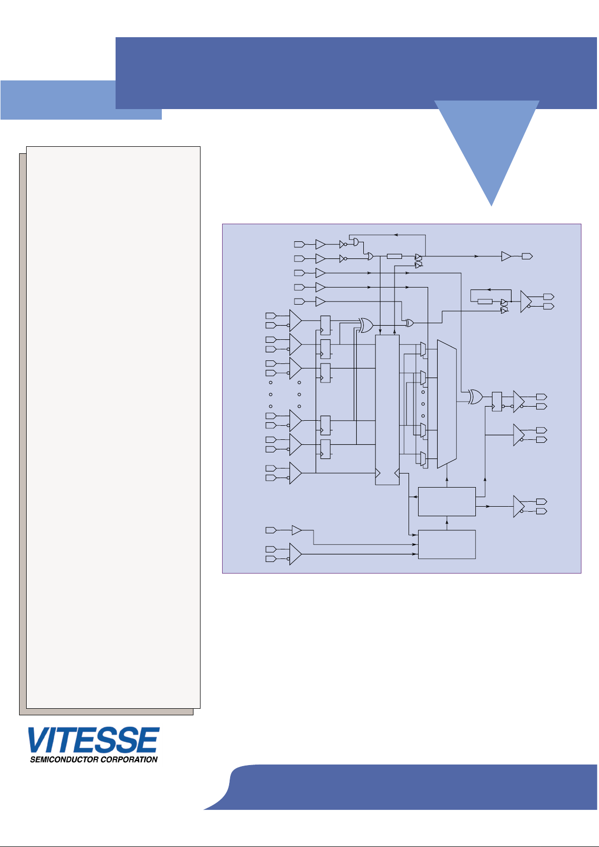
VSC8185 Block Diagram
Benefits:
• Provides High-speed Output
Clock for RZ and Re-timed
Laser Driver Applications
• Provides Lowest Power Solution
in its Performance Class
• Pin-compatible Path to 9.9 to
10.7Gb/s Product (VSC8175)
• Integrated PLL Based Clock
Generator
• True LVDS Parallel Data
Interface
• Thermal Expansion of TBGA
Package is Matched to the PC
Board for High Reliability
• Input FIFO to Simplify Parallel
Interface Timing
• Data Polarity Invert and Bit
Order Swap for Ease of Layout
Applications:
• Advanced Forward Error
Correction (FEC)
• Return-to-Zero Transmission
Applications
• Re-Timing Laser Drivers
• Ultra-Long Haul Systems
• SONET/SDH Networking
• DWDM Systems
• Telecommunications T ransmis-
sion Systems
• Test Equipment
PARSENSE
DINVALID+
DINVALID-
PARITY-
PARITY+
D1-
REFCK-
REFCK+
CK16_64+
CK16_64-
DCK-
DCK+
D14-
D14+
D0+
D0-
D1+
D15+
D15-
DOUT-
DOUT+
DINVERT
AUTORSTN
BITORDER
OVERFLOW
RESETN
COUT-
COUT+
16:1
PLL
FIFO
RST OVR
DELAY
GENERATOR
CK/16
TIMING
REFSEL
DELAY
11.5G-12.5G
719MHz/180MHz
 Loading...