

VITESSE VSC8184 Datasheet
11.5-12.5Gb/s 1:16 Demultiplexer with Clock Recovery
Physical
Layer
Products
Features:
• Continuous 1 1.5 to 12.5Gb/s
Lock-Range
• Low Power 1.6W (Typ)
• +3.3V Single Supply
• Single-End and Differential
Data Input
• 50 mV Input Sensitivity (Min)
• Slicing Threshold Voltage
Offset Control
VSC8184
Product Brief
• L VDS Outputs
• 180-195 or 719-781 MHz
Reference Clock
• Reliable 90-Ball BGA Package
• Up to 90°C Case Temperature
• On Chip Termination for all
L VDS Inputs
Specifications:
• 1 1.5 to 12.5 Gb/s Continuous
Lock-Range Operation
• 50 mV Input Sensitivity
• Supply Voltage: 3.3V (Typ)
• Total Power Dissipation:
1.6W (Typ)
• 15x15mm Low Profile 90 Ball
TBGA (Taped BGA) Package
• Operating Temperature Range:
0°C to +90°C (case)
General Description
The VCS8184 combines a clock recovery unit and data retiming with a
1:16 Demultiplexer on a single chip to
directly generate 16-bit wide data from
an incoming 1 1.5Gb/s to 12.5Gb/s data
stream, for use in SONET STS-192/
SDH STM-64 systems. An on-chip
Phase Locked Loop (PLL) with Voltage Controlled Oscillator (VCO) generates a 11.5GHz to 12.5GHz clock,
which remains phase locked to the incoming data. The incoming data is
retimed and Demultiplexer into 16 parallel outputs. It features a highly flexible reference clock input scheme. The
user can select between 180-195MHz
or 719-781MHz PECL reference clock
inputs. The input serial data sampling
point voltage threshold can be adjusted.
Additional features include a parity bit
(PARITY±) that is clocked out with the
16 parallel data, Bit Order Swap
(BITORDER) and Data Polarity Invert
(DINVERT). To assist in monitoring
device operation a Loss-of-Lock
(LOLN) alarm and no reference clock
(NOREFN) alarm are provided. The
device is packaged in a modified 90ball, Ball Grid Array (BGA).
www.vitesse.com
Physical Layer Products
11.5-12.5Gb/s 1:16 Demultiplexer with Clock Recovery
Product Brief
Benefits:
• Provides High-speed Integrated
Clock and Data Recovery from
1 1.5 to 12.5Gb/s
• Provides Lowest Power Solution
in its Performance Class
• Pin-compatible Path to 9.9-
10.7Gb/s Product (VSC8174)
• Thermal Expansion of TBGA
Package is Matched to the PC
Board for High Reliability
• Data Polarity Invert and Bit
Order Swap for Ease of Layout
• Loss-of-Lock and No Reference
Clock to Assist in Monitoring
Device Operation
• Parity Bit Calculation
• Integrated Clock and Data
Recovery
Applications:
• Advanced Forward Error
Correction (FEC)
• Return-to-Zero Transmission
Applications
• Re-Timing Laser Drivers
VSC8184
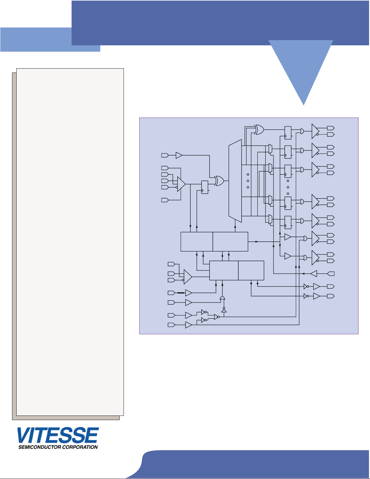
VSC8184 Block Diagram
DINVERT
OFF+
VTERM
DATA+
DATA-
OFF-
CLOCK
RECOVERY
REFTERM
REFCK+
REFCK-
REFSEL[0:1]
LCKREFN
INHIBITN
RESETN
1:16
TIMING
GENERATOR
PLL
LOSS
OF
LOCK
DETECT
Physical
Layer
Products
PARITY+
PARITY-
D0+
D0-
D1+
D1-
D14+
D14-
D15+
D15-
CK16A+
CK16A-
CK16B+
CK16B-
BITORDER
LOLN
NOREFN
• Ultra-Long Haul Systems
• SONET/SDH Networking
• DWDM Systems
• T elecommunications T ransmis-
sion Systems
• Test Equipment
www.vitesse.com
For more information on Vitesse Products visit the Vitesse web site
at www.vitesse.com or contact Vitesse Sales at (800) VITESSE or
sales@vitesse.com
© Copyright 2000 Vitesse Semiconductor Corporation
and the Vitesse logo
of Vitesse Semiconductor Corp;oration
are all registered trademarks
 Loading...