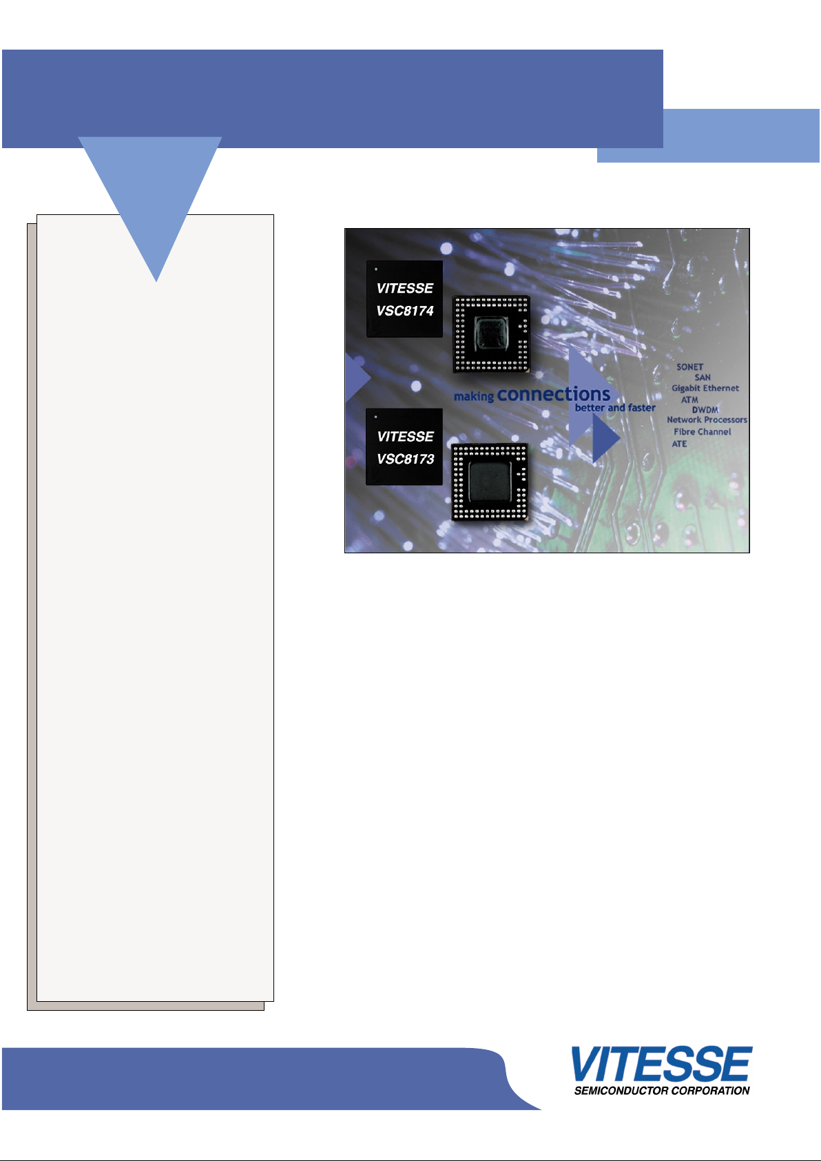
VITESSE VSC8174 Datasheet

www.vitesse.com
Product Brief
9.9-10.7Gb/s 1:16 Demultiplexer with Clock Recovery
Physical
Layer
Products
Physical Layer Products
VSC8174
General Description
The VSC8174 combines a clock recovery unit and data retiming with a
1:16 demultiplexer on a single chip to
directly generate 16-bit wide data from
an incoming 9.953 to 10.709Gb/s data
stream, for use in SONET STS-192/
SDH STM-64 systems. An on-chip
Phase Locked Loop (PLL) with Voltage Controlled Oscillator (VCO) generates a 9.953GHz to 10.709GHz
clock, which remains phase locked to
the incoming data. The incoming data
is retimed and demultiplexed into 16
parallel LVDS outputs. It features a
highly flexible reference clock input
scheme. The user can select between
19 to 21MHz, 155 to 168MHz or 622 to
670MHz reference clock inputs. The
input serial data sampling point voltage
threshold can be adjusted. Additional
features include a parity bit that is
clocked out with 16 parallel data, Bit
Order Swap and Data Polarity Invert.
To assist in monitoring device operation a Loss-of-Lock alarm and No-Reference-Clock alarm are provided. The
device is packaged in a modified 90Ball Grid Array (BGA).
Features:
• Continuous Lock-Range from
9.953-10.709Gb/s Rates
• Low Power 1.6W (Typ)
• +3.3V Single Supply
• Single-End and Differential
Data Input
• 10 mV Input Sensitivity (Min)
• Slicing Threshold Voltage
Offset Control
• True LVDS Outputs: No External
L VDS Terminations Required
• Fully Compliant with OIF 99.102
• SONET/SDH Jitter Compliant
• 19-21/155-168/622-670 MHz
Reference Clock Input
• Mode for 10.709Gb/s using
622MHz Reference Clock
• Reliable 90-Ball BGA Package
• Up to 90°C Case Temperature
Specifications:
• 9.953 to 10.709Gb/s Continuous
Lock-Range Operation
• 10 mV Input Sensitivity
• Supply Voltage: 3.3V (Typ)
• Total Power Dissipation:
1.6W (Typ)
• 15x15mm Low Profile 90 Ball
TBGA (Taped BGA) Package
• Operating Temperature Range:
0°C to +90°C (case)

For more information on Vitesse Products visit the Vitesse web site
at www.vitesse.com or contact Vitesse Sales at (800) VITESSE or
sales@vitesse.com
© Copyright 2000 Vitesse Semiconductor Corporation
and the Vitesse logo
are all registered trademarks
of Vitesse Semiconductor Corp;oration
www.vitesse.com
Product Brief
9.9-10.7Gb/s 1:16 Demultiplexer with Clock Recovery
VSC8174
Physical
Layer
Products
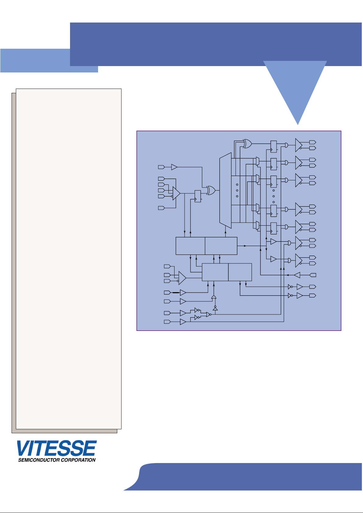
VSC8174 Block Diagram
Benefits:
• Provides Lowest Power Solution
in its Performance Class
• Pin-compatible Upgrade Paths
to Lower Power Follow-on
Product (VSC8174LP) and
Advance FEC (11.5 to 12.5Gb/s)
Product (VSC8184)
• Integrated Clock and Data
Recovery
• Meets SONET/SDH Jitter
Tolerance Requirements
• Input Data Sensitivity of
10 mV (Min)
• OIF 99.102 Compliant L VDS
Interface (No External Resistors
Required)
• Thermal Expansion of TBGA
Package is Matched to the PC
Board for High Reliability
• Loss-of-Lock and Internal
Temperature Sensing to Assist
in Monitoring Device Operation
• Data Polarity Invert and Bit
Order Swap for Ease of Layout
• Parity Bit Calculation
Applications:
• SONET/SDH Networking
• Transponder Modules
• DWDM Systems
• G.975/709 Forward Error
Correction (FEC)
• Gigabit Ethernet
• Telecommunications Transmis-
sion Systems
• Test Equipment
REFCK-
REFSEL[0:1]
RECOVERY
CLOCK
DATA-
DATA+
DETECT
LOCK
LOSS
OF
TIMING
GENERATOR
OFF+
OFF-
NOREFN
1:16
D0-
D0+
D1+
D1-
D15+
D15-
CK16A-
CK16A+
PARITY-
PARITY+
CK16B+
CK16B-
LOLN
BITORDER
DINVERT
D14-
D14+
PLL
RESETN
INHIBITN
LCKREFN
REFCK+
REFTERM
VTERM
 Loading...