


VITESSE VSC8173 Datasheet
www.vitesse.com
Product Brief
9.9-10.7Gb/s 16:1 Multiplexer with Clock Generator
Physical
Layer
Products
Physical Layer Products
VSC8173
General Description
The VSC8173 consists of a 16:1 multiplexer and a clock generator for use
in SONET STS-192/SDH STM-64 systems. The 16:1 multiplexer accepts 16
parallel LVDS inputs at a data rate of
622.08Mb/s to 669.31Mb/s. This parallel data stream is then serialized into
a 9.953Gb/s to 10.709Gb/s output.
Both 31 1MHz and 622MHz data clock
input modes are supported. The clock
generator creates the 9.953GHz to
10.709GHz clock signal used to retime the transmitted serialized data.
The clock generator requires a 155 to
168MHz or 622 to 670MHz PECL reference clock input. T o ease timing constraints on the parallel interface, a 16bit wide FIFO is included. A dividedby-16 or divide-by-64 LVDS clock output is available for use as a clock input
to the parallel data source. Additional
features include Bit Order Swap and
Data Polarity Invert. To assist in monitoring device operation a Loss-of-Lock
alarm and internal temperature sensing are provided. The device is packaged in a modified 90-Ball Grid Array
(BGA).
Features:
• Fully Compliant with OIF 99.102
• SONET/SDH Jitter Compliant
• 311MHz or 622MHz Data Clock
Input Modes
• Superior Data Output Eyes
• Low Power 1.5W (Typ)
• +3.3V Single Supply
• Continuous Tuning Operation
from 9.953 to 10.709Gb/s Rates
• 155-168/622-670 MHz
Reference Clock Input
• Reliable 90-Ball BGA Package
• Up to 90°C Case Temperature
Specifications:
• 9.953 to 10.709Gb/s Continuous
Operation
• Data Output Voltage Swing:
600mV (Min)
• Data Output Rise/Fall:
25ps (Typ)
• 10ps Wideband Jitter (Max)
• Supply Voltage: 3.3V (Typ)
• Total Power Dissipation:
1.5W (Typ)
• Operating Temperature Range:
0
°C to +90°C (case)
• 15x15mm Low Profile 90 Ball
TBGA (Taped BGA) Package
For more information on Vitesse Products visit the Vitesse web site
at www.vitesse.com or contact Vitesse Sales at (800) VITESSE or
sales@vitesse.com
© Copyright 2000 Vitesse Semiconductor Corporation
and the Vitesse logo
are all registered trademarks
of Vitesse Semiconductor Corp;oration
www.vitesse.com
Product Brief
9.9-10.7Gb/s 16:1 Multiplexer with Clock Generator
VSC8173
Physical
Layer
Products
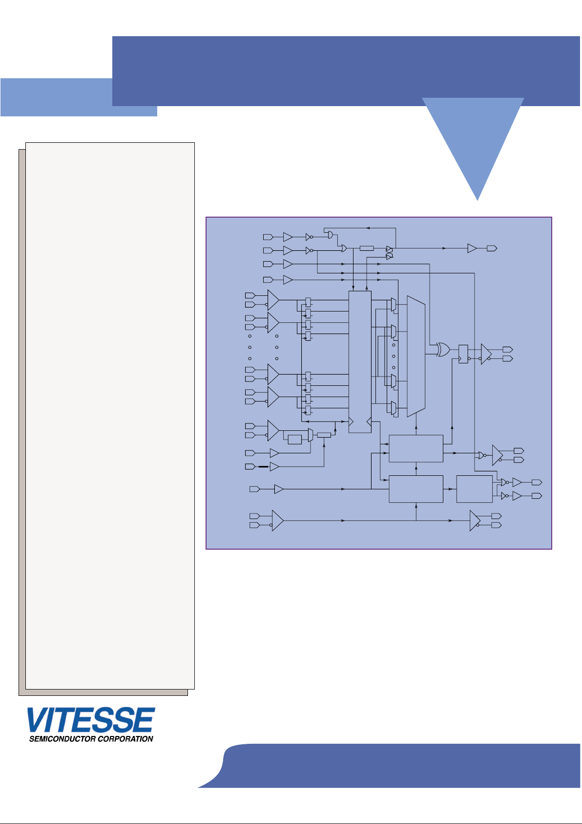
VSC8173 Block Diagram
Benefits:
• Provides Lowest Power Solution
in its Performance Class
• Pin-compatible Upgrade Paths
to Lower Power Follow-on
Product (VSC8173LP)
• Integrated PLL Based Clock
Generator
• Meets SONET/SDH Jitter
Generation Requirements
• OIF 99.102 Compliant L VDS
Interface
• Thermal Expansion of TBGA
Package is Matched to the PC
Board for High Reliability
• Input FIFO to Simplify Parallel
Interface Timing
• Loss-of-Lock and Internal
Temperature Sensing to Assist
in Monitoring Device Operation
• Data Polarity Invert and Bit
Order Swap for Ease of Layout
Applications:
• SONET/SDH Networking
• Transponder Modules
• DWDM Systems
• G.975/709 Forward Error
Correction (FEC)
• Gigabit Ethernet
• Telecommunications Transmis-
sion Systems
• Test Equipment
REFOUT+
REFOUT-
RESETN
OVERFLOW
BITORDER
AUTORSTN
DINVERT
REFSEL
CKMODE
2
DSKEW[0:1]
LOLN
NOREFN
DETECT
LOCK
LOSS
OF
DOUT+
DOUT-
D15-
D15+
D1+
D0-
D0+
D14+
D14-
DCK+
DCK-
16:1
TIMING
REFCK+
REFCK-
PLL
FIFO
9.9-10.7G
RST OVR
D1-
DELAY
GENERATOR
DELAY
DIV
CK/32
CK/16
CK16_64+
CK16_64-