

VITESSE VSC8169QR Datasheet
VITESSE
SEMICONDUCTOR CORPORATION
Preliminary Data Sheet
VSC8169
OC-48 (FEC) 16:1 SONET/SDH
MUX with Clock Generator
Features
• 16:1 Multiplexer Up to 2.7Gb/s
• Targeted for SONET OC-48 / SDH STM-16 (FEC)
Applications
• Differential LVPECL Low-Speed Interface
• On-Chip PLL-Based Clock Generator
• 128-Pin 14x20mm PQFP Package
• Single +3.3V Supply
General Description
The VSC8169 is a 16:1 multiplexer with integrated clock generator for use in SONET/SDH systems oper-
ating at a standard 2.48832Gb/s data rate or a forward error correction (FEC) data rate up to 2.7Gb/s. The internal clock generator uses a Phase-Locked Loop (PLL) to multiply either a 77.76MHz (up to 84.38MHz-FEC) or
a 155.52MHz (up to 168.75MHz -FEC ) reference clock in order to provide the 2.48832GH z (up to 2.7G Hz FEC) clock for internal logic and outp ut retiming. For use with th e VSC9210 FEC Encoder/ Decoder chipset
running at 2.654208Gb/s, a refer ence clo ck of 82.9 44MHz (seri al rate di vided by 32) should be used. The 16 -bit
parallel interface incorporates an on-board FIFO eliminating loop timing design issues by providing a flexible
parallel timing architecture. The device operates using a 3.3V power supply, and is packaged in a thermallyenhanced plastic package. The thermal performance of the 128-pin PQFP allows the use of the VSC8169 without a heat sink under most thermal conditions.
VSC8169 Block Diagram
CLK16I+
CLK16I-
D0+
D0-
D15+
D15-
REFCLKO+
REFCLKO-
Reset
CLK16O+
CLK16O-
REFCLK+
REFCLK-
F_FREQSEL
Input Register
Divide
by 2
Write
Pointer
16x5 FIFO
Read
Pointer
Divide by 16
2.6GHz
PLL
FIFO
Control
Output
Retime
DO+
DO-
CLKO+
CLKO-
FIFO_WAR
G52230-0, Rev 3.6 Page 1
01/02/01
© VITESSE SEMICONDUCTOR CORPORATION • 741 Calle Plano • Camarillo, CA 93012
Tel: (800) VITESSE • FAX: (805) 987-5896 • Email: prodinfo@vitesse.com
Internet: www.vitesse.com
VITESSE
SEMICONDUCTOR CORPORATION
OC-48 (FEC) 16:1 SONET/SD H
MUX with Clock Generator
Preliminary Data Sheet
VSC8169
Functional Description
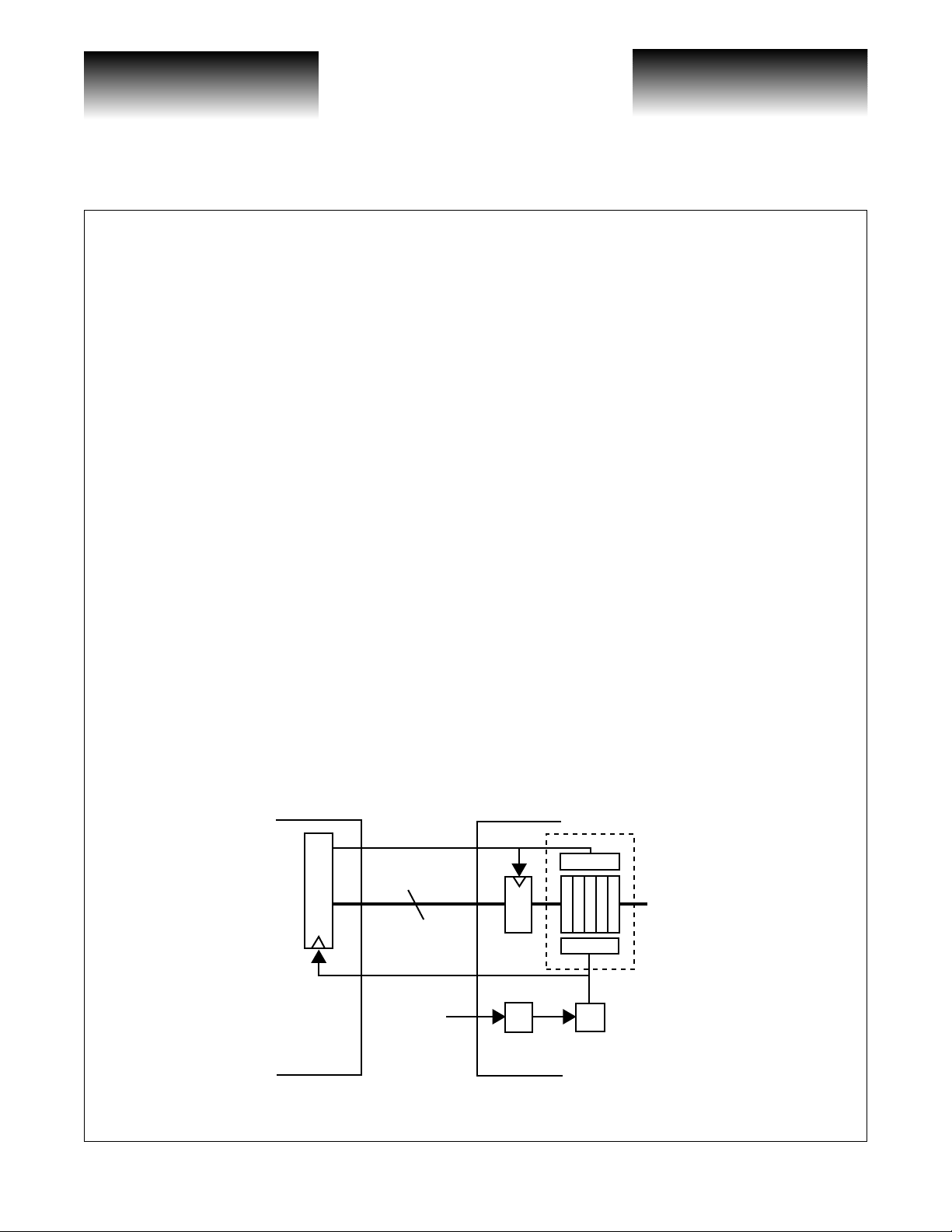
Low-Speed Interface
The Upstream Device should use the CLK16O as the timing source for its final output latch (see Figure 1).
The Upstream Device should then generate a CLK16I that is phase aligned with the data. The VSC8169 will
latch D[15:0]
CLK16I (see Table 2). In addition to the CLK16O clock output, there also exi sts a utili ty REFCLKO output signal, which is a clock with the same rate as that presented at the REFCLK input.
A FIFO exists within the VS C8169 to elimina te difficult system loop timing issues . Once the PLL h as
locked to the reference clock, RESET must be held low for a minimum of five CLK16 cycles to initialize the
FIFO, then RESET should be set high and held constant for continuous FIFO operation. For the transparent
mode of operation (no FIFO), simply hold RESET at a constant low state (see Figure 2).
The use of a FIFO permits the system designer to tolerate an arbitrary amount of delay between CLK16O
and CLK16I. Once RESET is asserted and the FIFO initialized, the delay betw een CLK16O and CLK16I can
decrease or increase up to one period of the low-speed clock (6.4ns). Should this delay drift exceed one period,
the write pointer and the read pointer could point to the same word in the FIFO, resulting i n a loss of transmitted
data (a FIFO overflow). In the event of a FIFO overflow, an active low FIFO_WARN signal is asserted (for a
minimum of five CLK16I cycles) which can be used to initiate a reset signal from an external controller.
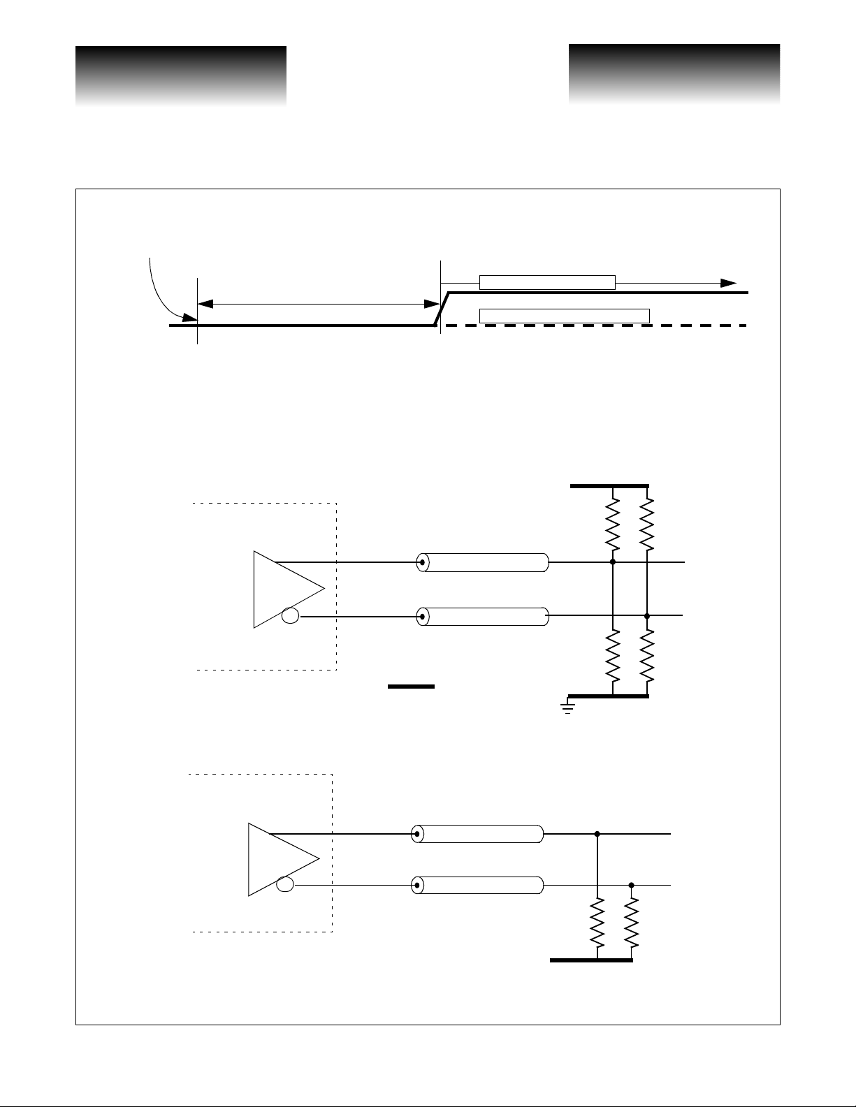
The CLK16O
transmission line can be DC terminated with a split-end termin ation scheme (see Fig ure 3), or DC terminated by
50
Ω to V
substituted for the traditional 50
ods. Figure 5 illustrates an example AC-coupling method for the occasion when the downstream device provides the bias point for AC-coupling. If the downstream device were to have interna l termination, the line to
line 100
± on the rising edge of CLK16I+. The da ta must meet setup and hold times with respect to
± output driver is a LVPECL output driver designed to drive a 50Ω transmission line. The
-2V on each line (see Figure 4). At any time, the equivalent split-end termination technique can be
CC
Ω to V
Ω resistor may not be necessary.
-2V on each line. AC-coupling can be achieved by a number of meth-
CC
Figure 1: Low-Speed Systems Interface
CLK16I
x16
Upstream
Device
CLK16O
REFCLK
2.6GHz
PLL
Page 2 G52230-0, Rev 3.6
© VITESSE SEMICONDUCTOR CORPORATION • 741 Calle Plano • Camarillo, CA 93012
Tel: (800) VITESSE • FAX: (805) 987-5896 • Email: prodinfo@vitesse.com
Internet: www.vitesse.com
Write
Read
16 x 5 FIFO
VSC8169
Divide by 16
01/02/01
VITESSE
SEMICONDUCTOR CORPORATION
Preliminary Data Sheet
VSC8169
PLL locked to reference clock.
Minimum 5 CLK16 cycles
RESET
Holding RESET “low” for a minimum of 5 CLK16 cycles, then setting “high” enables FIFO operation.
Holding RESET constantly “low” bypasses the FIFO for transparent mode operation.
Figure 3: Split-End DC Termination of CLK16O+/-, REFCLKO+/-
VSC8169
Figure 2: Enabling FIFO Operation
FIFO Mode Operation
Transparent Mode Operation
Split-end equivalent termination is ZO to V
R1 = 125Ω R2 = 83Ω, Zo=50Ω, V
Z
o
TERM
TERM
= VCC-2V
OC-48 (FEC) 16:1 SONET/SDH
MUX with Clock Generator
V
CC
R1
R1
Z
o
R1||R2 = Z
VCCR2 + VEER1
R1+R2
O
= V
TERM
V
EE
R2
Figure 4: Traditional DC Termination of CLK16O+/-, REFCLKO+/-
VSC8169
Z
O
Z
O
50Ω
VCC-2V
R2
50Ω
G52230-0, Rev 3.6 Page 3
01/02/01
© VITESSE SEMICONDUCTOR CORPORATION • 741 Calle Plano • Camarillo, CA 93012
Tel: (800) VITESSE • FAX: (805) 987-5896 • Email: prodinfo@vitesse.com
Internet: www.vitesse.com
VITESSE
SEMICONDUCTOR CORPORATION
OC-48 (FEC) 16:1 SONET/SD H
MUX with Clock Generator
Figure 5: AC Termination of CLK16O+/-, REFCLKO+/-
VSC8169
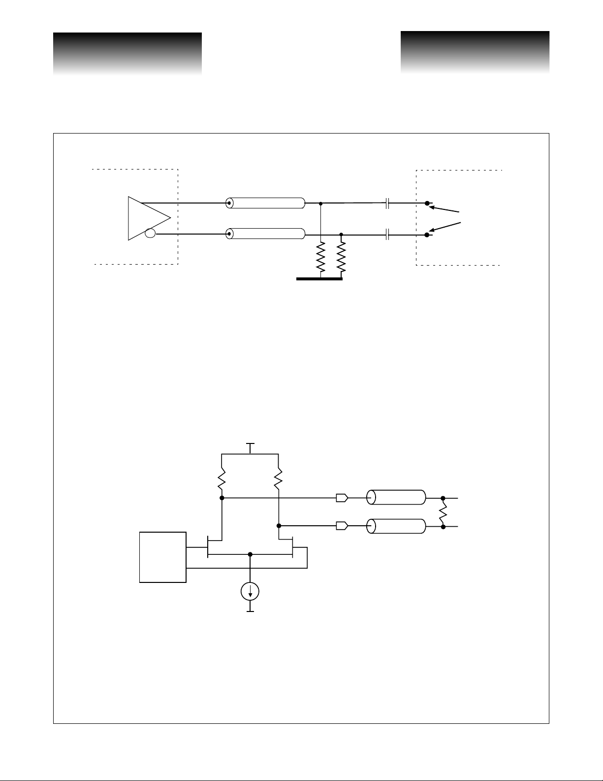
High-Speed Data and Clock Output
The high-speed data and clock outpu t driver s consist of a dif f erenti al pair desi gned to dri ve a 50Ω tran s mis-
sion line. The transmission line should be terminated with a 100
ment outputs (see Figure 6). Connection to a termination voltage is not required. The output driver is back
terminated to 50
driver must still be terminated differentially at the load with a 100
puts. The high-speed clock output can be powered down for additi onal power savi ngs. To power down the highspeed clock, tie the associated pins to V
Ω on-chip, providing a snubbing of any refl ect ion s . If used sin gle- ended , the high-speed output
Z
o
Z
o
50Ω
(see Table 3, Package Pin Id entifications, pins 5,6,7).
CC
50Ω
V
CC
Ω resistor at the load between true and comple-
Ω resistor between true and complement out-
Preliminary Data Sheet
VSC8169
100nF
100nF
-2V
downstream
bias point
generated
internally
Figure 6: High-Speed Output Termination
V
CC
50Ω
Pre-Driver
V
EE
Clock Generator
An on-chip PLL generates the 2.48832GHz (or up to 2.7GHz for FEC) transmit clock from the externally
provided REFCLK input. The on-chip PLL uses a low phase noise reactance-based Voltage Controlled Oscillator (VCO) with an on-chip loop filter. The loop bandwidth of the PLL is within the SONET specified limit of
2MHz.
50Ω
100Ω
Z0 = 50Ω
Page 4 G52230-0, Rev 3.6
© VITESSE SEMICONDUCTOR CORPORATION • 741 Calle Plano • Camarillo, CA 93012
Tel: (800) VITESSE • FAX: (805) 987-5896 • Email: prodinfo@vitesse.com
Internet: www.vitesse.com
01/02/01
VITESSE
SEMICONDUCTOR CORPORATION
Preliminary Data Sheet
VSC8169
OC-48 (FEC) 16:1 SONET/SDH
MUX with Clock Generator
The customer can select to provide either a 77.76MHz (up to 84.38MHz- FEC) reference (recommended),
or the 2x of that reference, 155.52MHz (up to 168.75MHz-FEC). REF_FREQSEL is used to select the desired
reference frequency. REF_FREQSEL = “0” designates REFCLK
input as 77.76MHz (up to 84.38MHz-FEC),
REF_FREQSEL = “1” designates REFCLK input as 155.52MHz (up to 168.75MHz - FEC) . For use with the
VSC9210 FEC Encoder/Decoder chipset running at 2.654208Gb/s, REF_FREQSEL = “0” should be selected
with the REFCLK
input as 82.944MHz (serial rate divided by 32).
The REFCLK should be of high quality since noise on the REFCLK below the loop band width of the PLL
will pass through the PLL and appear as jitter on the output. Preconditioning of the REFCLK signal with a
VCXO may be required to avoid passing REFCLK noise with greater than 4ps RMS of jitter to the output. The
VSC8169 will output the REFC LK noise in add ition to the intr insic jitte r from the VSC816 9 itself duri ng such
conditions.
Low-Speed Inputs
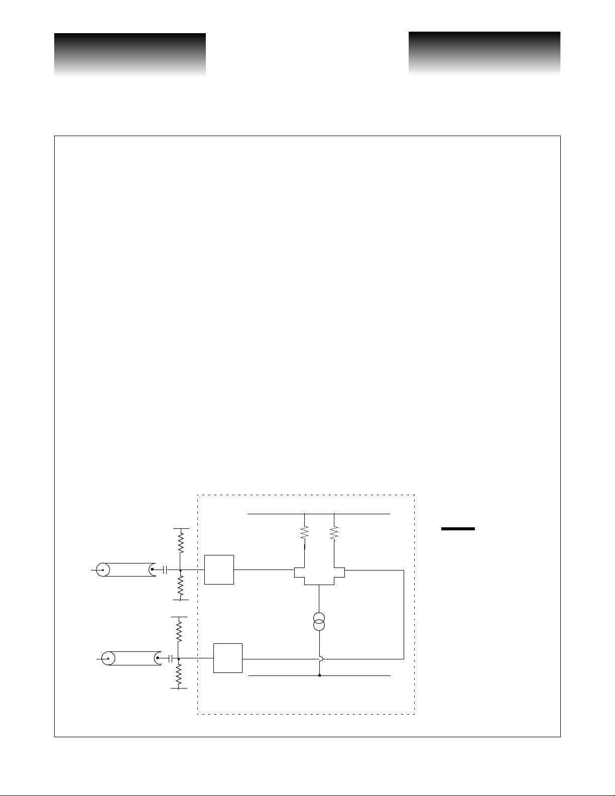
The incoming low-speed data and reference clock input are received by LVPECL inputs D[15:0] and REFCLK. Off-chip termination of these inputs is required. For AC-coupling, a bias voltage suitable for AC-coupling needs to be provided. See Figure 7 for external biasing resistor scheme..
In most situations these inputs will have high transition density and little DC offset. However, in cases
where this does not hol d, d irect DC con nect io n i s possi bl e. Al l ser ia l d at a i nputs have the same circuit topology,
as shown in Figure 7. If the input signal is dri ven dif feren tial ly and DC-cou pled to the part, t he mid-poi nt of the
V
input signal swing should be centered a bout this common mode reference voltage (
) and not exceed the
CMI
maximum allowable amplitude. For single -ended , DC-coupli ng operati ons, it is recommend ed that th e user provides an external reference voltage. The external reference should have a nominal value equivalent to the common mode switch point of the DC-coupled signal, and can be connected to either side of the differential gate.
Figure 7: AC Termination of Low-Speed LVPECL REFCLK, D[15:0] Inputs
Split-end equivalent te r m ination is ZO to V
Chip Boundary
VCC = 3.3V
V
CC
R1
Z
O
Z
C
IN
EE
CC
C
EE
R2
R1
IN
R2
VEE = 0V
V
V
O
V
R1 = 83Ω R2 = 125Ω, Zo=50Ω, V
R1||R2 = Z
VCCR2 + VEER1
O
R1+R2
TERM
= V
TERM
= VCC-2V
Term
CIN TYP = 100nF
for AC operation
G52230-0, Rev 3.6 Page 5
01/02/01
© VITESSE SEMICONDUCTOR CORPORATION • 741 Calle Plano • Camarillo, CA 93012
Tel: (800) VITESSE • FAX: (805) 987-5896 • Email: prodinfo@vitesse.com
Internet: www.vitesse.com
VITESSE
SEMICONDUCTOR CORPORATION
OC-48 (FEC) 16:1 SONET/SD H
MUX with Clock Generator
Supplies
Preliminary Data Sheet
VSC8169
The VSC8169 is specified as a LVPECL device with a single positive 3.3V supply. Should the user desire
to use the device in an ECL en viro nment wit h a n egat i ve 3.3 V su pply, then V
-3.3V. If used with V
tied to -3.3V, the TTL control signals are still referenced to VEE.
EE
will be ground and VEE will be
CC
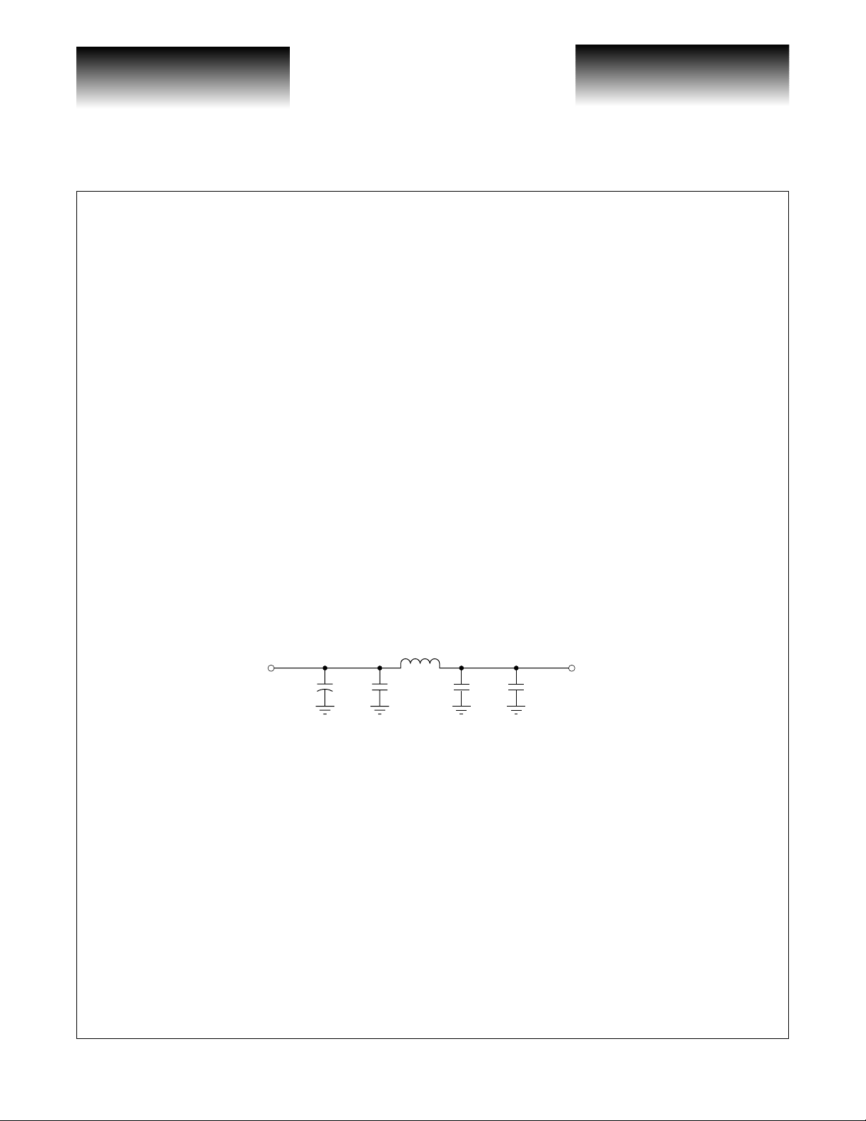
Decoupling of the power supplies is a critical element in maintaining the proper operation of the part. It is
recommended that the V
on each V
power supply pin as close to the package as possible. If room permits, a 0.001µF capacitor should
CC
also be placed in parallel with the 0.1
low-inductance ceramic SMT X7R devices. For the 0.1
0.01
µF and 0.001µF capacitors can be either 0603 or 0402 packages.
Extra care needs to be taken when decoupling the analog power supply pins (labeled V
power supply be decoupled using a 0.1µF and 0.01µF capacitor placed in parallel
CC
µF and 0.01µF capacitors mentioned above. Recommended capacitors are
µF capacitor, a 0603 package should be used. The
). In order to
CCANA
maintain the optimal jitter and loop bandwidth characteristics of the PLL contained in the VSC8169, the analog
power supply pins sh ould be filtered fr om the main pow er supply with a 10
ferrite bead may be used to provide the isolation. The 0.1
µF and 0.01µF decoupling capacitors are still required
µH C-L-C pi filter. If preferred, a
and must be connected to the supply pins between the device and the C-L-C pi filter (or ferrite bead).
For low frequency decoupling, 47
µF tantalum low inductance SMT caps are sprinkled over the board’s
main +3.3V power supply and placed close to the C-L-C pi filter.
If the device is being used in an ECL environment with a -3.3V supply, then all references to decoupling
V
must be changed to VEE, and all references to decoupling 3.3V must be changed to -3.3V.
CC
Figure 8: PLL Power Supply Decoupling Scheme
10 H
V
CC
10 F
0.1 F
V
EE
V
EE_ANA
0.01 F0.1 F
V
CC_ANA
Page 6 G52230-0, Rev 3.6
© VITESSE SEMICONDUCTOR CORPORATION • 741 Calle Plano • Camarillo, CA 93012
Tel: (800) VITESSE • FAX: (805) 987-5896 • Email: prodinfo@vitesse.com
Internet: www.vitesse.com
01/02/01
 Loading...