

VITESSE VSC8166 Datasheet

VITESSE
SEMICONDUCTOR CORPORATION
Preliminary Datasheet
SC8166
1:16 SONET/SDH Demux with Clock Recovery
2.488 Gbit/sec
Features
• 2.488Gb/s 1:16 Demultiplexer
• Fully Integrated Clock and Data Recovery
• Single 3.3V Supply Operation
• Differential LVPECL Low Speed Interface
• Maintains Clock Output in the Absence of
Data
• Loss of Lock, Loss of Signal Indicators
• 128 Pin 14x20x2 mm Enhanced PQFP Pkg.
• 2.3W Max Power Dissipation
General Description
The VSC8166 demultiplexes a 2.488Gbp/s LVPECL serial input datastream (DI+) to 16-bit wide, LVPECL
155Mb/s parallel data outputs (D0:D15+
recovery unit with an on-chip PLL th at in tern ally g enera tes a 2. 488GHz clo ck in pha se with the incom ing data .
Internal divider circuits are used to take the high-speed clock and generate 155.52MHz (CLK16O+
77.76MHz (CLK32O+
) LVPECL external out put c locks . The inc oming data is re time d and demu ltip lexed to a
16-bit word which is clocked out of the demultiplexer by the 155.52MHz output clock.
Alarm functions support typical telecom system applications. A TTL Loss Of Lock (LOL) indicator can be
externally enabled (LOLEN) to detect when the device goes out of lock, which would most often occur in the
event of a loss of valid data. A TTL No-Reference (NOREF) output indicator flags when the LVPECL Clock
Reference (REFCLK) input to the VSC8166 either is removed, or goes severely out of tolerance. For Loss Of
Signal (LOS) conditions from an Optics Module, the VSC8166 provides a polarity (POL) input to accommodate any polarity differences.
Only a single 3.3V power supply is required for device operation and the device is packaged in a thermally
enhanced 128 Pin 14x20x2 mm PQFP Package.
) for SONET/SDH applications. It has an integrated clock and data
) and
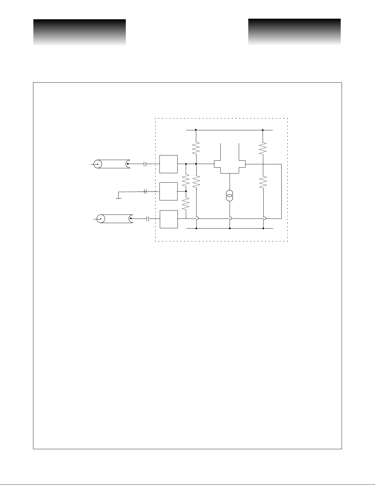
VSC8166 Block DIagram
1:16 DMUX
DI+
DI-
REFCLK+
REFCLK-
POL
LOS
LOLEN
G52252-0, Rev. 3.0
11/9/99 741 Calle Plano, Camarillo, CA 93012 • 805/388-3700 • FAX: 805/987-5896
Clock
Recovery
VITESSE SEMICONDUCTOR CORPORATION
Data
Re-time
Divide
by 16
Divide
by 2
1
0
Output Register
D0+
D0-
D15+
D15-
CLK16O+
CLK16O-
CLK32O+
CLK32O-
NOREF
LOL
Page 1

VITESSE
t
SEMICONDUCTOR CORPORATION
2.488 Gbit/sec
1:16 SONET/SDH Demux with Clock Recovery
Preliminary Datashee
VSC8166
Functional Description
Clock Recovery:
The incoming SONET/SDH data stream is fed both to a re-timing latch and to the integrated clock recovery
unit (CRU). The CRU exceeds the SONET/SDH jitter tolerance map. A 77.76MHz reference clock (REF -
) is required for CRU operation. Off-chip termination of this input is required. For AC coupling, a bias
CLK+
voltage suitable for AC coupling needs to be provided, see Figure 1 for biasing scheme. The 77.76MHz reference is used to permit the CLK16O+
Figure 1: AC Termination of LVPECL REFCLK Input
V
CC
R1
Z
O
C
IN
to remain locked to this external reference clock in the event of data loss.
Split-end equivalent termination is Zo to V
Chip Boundary
VCC = 3.3V
R1 = 125Ω, R2 = 83Ω, Zo=50Ω, V
R1||R2 = Z
R2 + VEER1
V
CC
R1+R2
= VCC-2V
Term
o
= V
Term
Bias
EE
CC
C
EE
R2
R1
IN
R2
VEE = 0V
V
V
Z
O
V
CIN TYP = 100 nF
for AC operation.
The VSC8166 has a TTL input LOS to force the part into a Loss of Signal state. Most optics have a TTL
output usually called “S D” (Si gnal Det ect), based o n t he op ti cal power of the incoming light st ream. Depen di ng
on the optics manufact urer, this signal is either a ctive high or low. To accom modate polarity differences, the
internal Loss of Signal i s generated when the POL and LOS inputs are of o pposi te st at es. Once active, all zer oes
“0” will be propagated downstream using the transmit clo ck until the optical signa l is regained and LOS and
POL are in the same logic state. When LOS and POL are opposite logic states, an internal LOS is asserted and
all output data D(0:15)+
will go to zero on the next rising edge of CLK16O+.
If LOLEN is low, and the serial input data consists of 3.3us or more of continuous zeros, LOL will go high
and remain high for 100us fol lowing the restoratio n of valid data. If LOLEN is high , loss of data loc k “OR”
3.3us of zeros will cause LOL to go high and remain high for 100us after both the return of non-zero data, and
phase locking of the Serial data and clock are obtained.
NOREF will go high asynchronously when R EFCLK is lost , or when REFC LK i s not locked to the internal
2.488GHZ clock. It will remain high until the condition is corrected.
Page 2
741 Calle Plano, Camarillo, CA 93012 • 805/388-3700 • FAX: 805/987-5896 11/9/99
VITESSE SEMICONDUCTOR CORPORATION
G52252-0, Rev 3.0
VITESSE
SEMICONDUCTOR CORPORATION
Preliminary Datasheet
SC8166
Low Speed Interface
1:16 SONET/SDH Demux with Clock Recovery
2.488 Gbit/sec
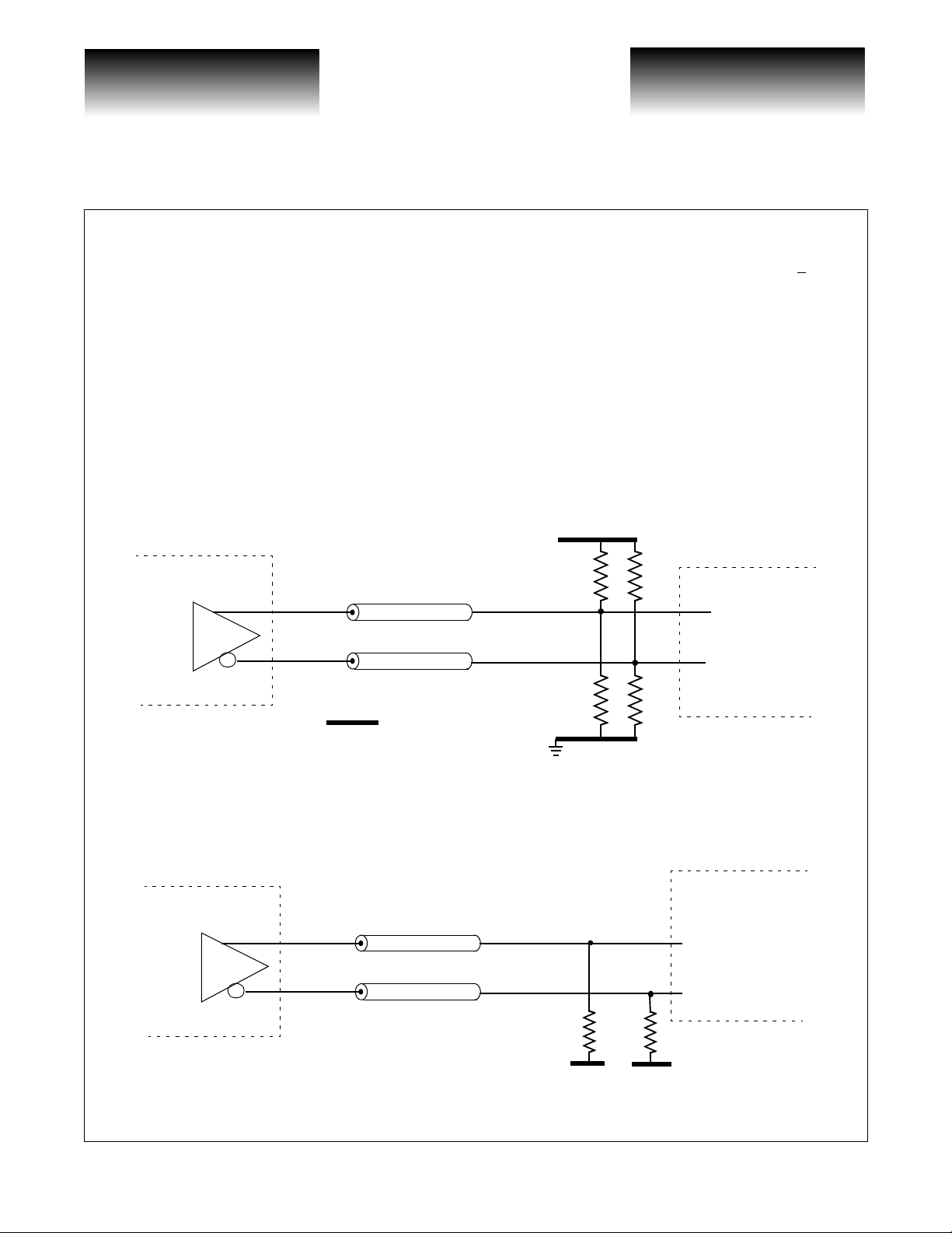
The demultiplexed serial stream is made available by a 16 bit differential LVPECL interface D(15:0)+ with
accompanying differential LVPECL divide by 16 clock CLK16O
± and divide by 32 clock CLK32O±. The low
speed LVPECL output drivers are designed to drive a 50Ω transmission line. The transmission line can be DC
terminated with a split end termination scheme, see Figure 2, or DC terminated by 50Ω to V
-2V on each line,
CC
see Figure 3. At any time, the eq uivalent split-end termination technique can be subs tituted for the traditional
50Ω to V
-2V on each line. AC coupling can be achieved b y a n umber of met hod s. F igure 4 i llustrat es an AC
CC
coupling method for the occasion when the downstream device provides the bias point for AC coupling. If the
downstream device were to have internal termination, the line to line 100Ω resistor may not be necessary. The
divide by 32 output can be used to provide a reference clock for the clock multiplication unit on the VSC8163.
Figure 2: Split-end DC Termination of Low Speed LVPECL CLK16O, CLK32O, D[15:0] Outputs
Term
VCC
R1
R1
downstream
VSC8166
Split-end equivalent termination is Zo to V
R1 = 125Ω R2 = 83Ω, Zo=50Ω, V
Z
o
Term
= VCC-2V
Z
R1||R2 = Z
R2 + VEER1
V
CC
R1+R2
Figure 3: Traditional DC Termination of Low Speed LVPECL CLK16O, CLK32O, D[15:0] Outputs
o
o
= V
Term
VEE
R2
R2
downstream
VSC8166
Z
o
R1 =50Ω
VCC-2V
R1 =50Ω
VCC-2V
G52252-0, Rev. 3.0
11/9/99 741 Calle Plano, Camarillo, CA 93012 • 805/388-3700 • FAX: 805/987-5896
VITESSE SEMICONDUCTOR CORPORATION
Page 3
VITESSE
t
SEMICONDUCTOR CORPORATION
2.488 Gbit/sec
1:16 SONET/SDH Demux with Clock Recovery
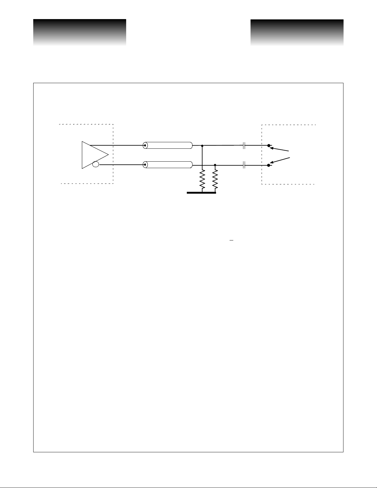
Figure 4: AC Termination of Low Speed LVPECL CLK16O, CLK32O, D[15:0] Outputs
VSC8166
High Speed Interface
The incoming 2.488G b/s data is re ceived by high speed inputs DI +. The data inp uts are internally terminated by a center-tapped resistor network. For differential input DC coupling, the network is terminated to the
appropriate termination voltage V
and complement inputs. For differential input AC coupling, the network is terminated to V
capacitor.
In most situations these inputs will have high transition density and little DC offset. However, in cases
where this does not hold, di rect DC con nect i on is possi ble. Serial data inputs ha ve the circuit topolog y sh own in
Figure 5. The reference voltage is created by a resistor divider as shown. If the input signal is driven differentially and DC-coupled to the part, the mid-point of the input signal swing should be centered about this reference voltage and n ot e xc eed t he maxi mum al l owable amplitude (
operations, it is recommended that the user provides an external reference voltage which has better temperature
and power supply noise r ejecti on than th e on-chip r esistor divider. The external re ference sho uld ha v e a nominal
value equivalent to the common mode switch point of the DC coupled signal, and ca n be connec ted to either
side of the differential gate.
TERM
Z
o
Z
o
50
∆V
V
CMI
Ω
CC
, ∆V
-2V
50
Ω
(pins HSDREF) providing a 50Ω to V
Preliminary Datashee
VSC8166
0.1uF
0.1uF
TERM
). For single-ended, DC-coupling
IHS
downstream
bias point
generated
internally
termination for both true
via a blocking
TERM
Page 4
741 Calle Plano, Camarillo, CA 93012 • 805/388-3700 • FAX: 805/987-5896 11/9/99
VITESSE SEMICONDUCTOR CORPORATION
G52252-0, Rev 3.0
VITESSE
SEMICONDUCTOR CORPORATION
Preliminary Datasheet
SC8166
Z
O
V
Z
O
1:16 SONET/SDH Demux with Clock Recovery
Figure 5: High Speed Serial Data Inputs
Chip Boundary
VCC = 3.3V
C
IN
50
Ω
50
Ω
Term
C
AC
C
IN
2.488 Gbit/sec
VEE = 0V
TYP = 100 pF
C
IN
TYP = 100pF
C
AC
Supplies
This device is specified as a LVPECL device with a single positive 3.3V supply. Should the user desire to
use the device in a ECL environment with a negative 3.3V supply, then VCC will be ground and VEE w ill be -
3.3V.
Decoupling of the power supplies is a critical element in maintaining the proper operation of the part. It is
recommended that the V
each V
power supply pin as close to the package as possible. If room permits, a 0.001µF capacitor should
CC
power supply be d ecoup led using a 0.1µF and 0.01µF capacitor placed in parallel on
CC
also be placed in parallel with the 0.1µF and 0.01µF capacitors mentioned above. Recommended capacitors are
low inductance ceramic SMT X7R devices. For the 0.1µF capacitor, a 0603 package should be used. The
0.01µF and 0.001µF capacitors can be either 0603 or 0403 packages.
For low frequency decoupling, 47µF tantalum low inductance SMT caps should be sprinkled over the
board’s main +3.3V power supply and placed close to the C-L-C pi filter.
If the device is being used in an E CL environment with a -3.3V supply, then all references to decoupling
must be changed to VEE, and all references to decoupling 3.3V must be changed to -3.3V.
V
CC
G52252-0, Rev. 3.0
11/9/99 741 Calle Plano, Camarillo, CA 93012 • 805/388-3700 • FAX: 805/987-5896
VITESSE SEMICONDUCTOR CORPORATION
Page 5
 Loading...