

VITESSE VSC8162 Datasheet
A
VITESSE
SEMICONDUCTOR CORPORATION
dvance Product Information
SC8162
2.488 Gbit/sec SONET/SDH
1:16 Demux with Clock Recovery
Features
• 2.488Gb/s 1:16 Demux with Integrated Clock and
Data Recovery
• Recovered Clock and Data Available
• Monolithic Phase Locked Loop
• Digitally Adjustable Serial Data Sampling Point
• Differential Low Speed Outputs
• Differential/Single-ended Reference Clock
• Loss of Lock Detection
• Meets SONET OC-48 and SDH STM-16 Jitter
Tolerance Requirements
General Description
The VSC8162 combines a clock recovery unit (CRU) with a 1:16 demultiplexer on a single chip to directly
generate 16-bit wide data from an incoming 2.488Gb/s NRZ data stream. An on-chip Phase Locked Loop (PLL)
generates a 2.488GHz clock which remains phase locked to the incoming data. The incoming data is retimed
and demultiplexed to a 16-bit word. A Loss of Lock (LOL) signal indicates gross conditions where incoming
data no longer has sufficient transitions to keep the CRU in lock.
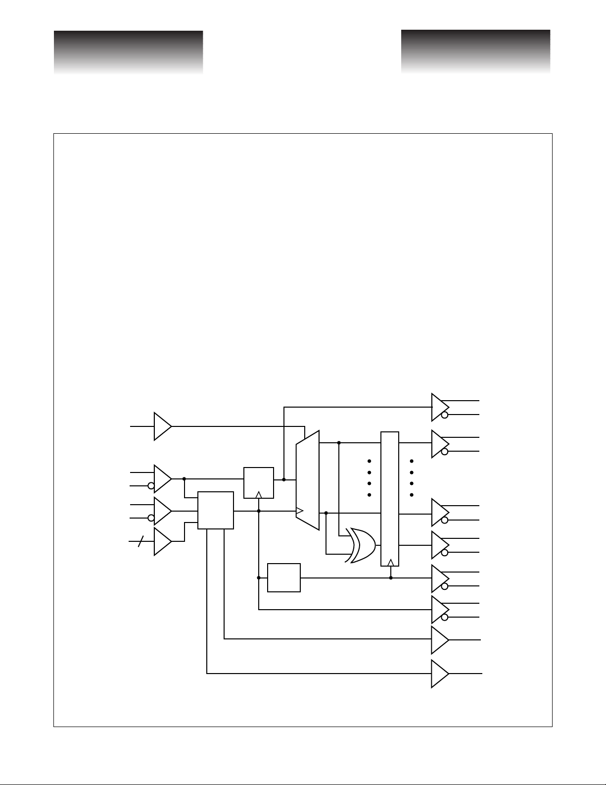
VSC8162 Functional Block DIagram
DINVERT
DI+
DI–
REFCK+
REFCK–
PADJ[4:0]
RTDO+
RTDO–
D0+
D0–
Data
Retime
Clock
Recovery
5
Divide
by 16
Output Register
D15+
D15–
PARITY+
PARITY–
CLK16+
CLK16–
CLKO+
CLKO–
LOL
NOREF
G52209-0, Rev. 2.0
9/14/98 741 Calle Plano, Camarillo, CA 93012 • 805/388-3700 • FAX: 805/987-5896
VITESSE
SEMICONDUCTOR CORPORATION
Page 1

VITESSE
SEMICONDUCTOR CORPORATION
2.488 Gbit/sec SONET/SDH
1:16 Demux with Clock Recovery
Advance Product Information
VSC8162
Functional Description
Clock Recovery:
The clock recovery unit (CRU) consists of a phase detector, voltage controlled oscillator (VCO), loop filter
and frequency control unit (FCU). The components of the CRU are fully integrated on the VSC8162. A
19.44MHz reference clock (REFCLK) is required for proper operation of the Clock Recovery Unit (CRU). Jitter tolerance of the CRU is well above the SONET and SDH jitter tolerance masks. In addition, the recovered
high speed clock is output on the CLKO pins.
Incoming data is presented to both the clock recovery circuit and the data retiming circuit. When the CRU is
in lock mode, a phase detector circuit is effective. When there is a phase error between the incoming data and
the on-chip VCO, the phase detector output raises or lowers the voltage on the loop filter to null the phase difference.
The frequency control unit (FCU) monitors the frequency difference between the reference clock, REFCK,
and the recovered clock. At the time that the VCO frequency,
differ by less than 1 MHz, the FCU only passively monitors the frequency difference continuously without
sending any corrections to the loop filter. In the event of the loss of an input signal, or if the input is switching
randomly, the VCO will drift in one direction. At the time that
the FCU will maintain the VCO frequenc y to be at approximately 1MHz of f the frequency of
lock detector will assert the LOL output. LOL is designed to be asserted from between 2.3us and 100us after the
interruption of data.
When NRZ data is again presented at the data input, the phase detector will permit the VCO to lock to the
incoming data. Hysteresis is provided which delays the deassertion of LOL until approximately 160us following the restoration of valid data.
The NOREF output will go high to indicate that there is no signal on the REFCK input, or that the REFCK
is more than approximately 25% above or below the expected value.
f
, and the 128x REFCK frequency,
VCO
and
128
x
f
differ by more than 1 MHz,
REF
f
VCO
128
128
x
f
REF
x
f
REF
, and the
,
Retiming:
The retiming decision circuit functions as a D Flip Flop. The recovered clock nominally clocks the decision
circuit in the center of the data eye. Internally , the reco v ered clock is duplicated to create 32 copies, with a phase
difference between each of 1/32 of a unit interval. The PADJ[4:0] inputs select which of the 32 phases are to be
used to retime the data. Certain lightwave systems employing optical amplifiers suffer from noise in the leading
edge of the data eye. Therefore these systems may achieve their lowest Bit Error Rate (BER) by delaying the
retiming point until later in the eye. The PADJ inputs can be strapped to generate a fixed delay or the customer
can develop a dynamic circuit which can select the optimum retiming point during a training sequence. The
retimed high speed data can be monitored using the RTDO pins.
Figure 1 and Table 1 indicate how the PADJ pins adjust the sampling point in the data eye. The step size of
each unit interval is approximately 12.5ps. The values in Table 1 are not exact and should be used only as an
approximation of the expected delay. Due to environmental variations, the actual measured value at any point
could vary by as much as +/- 1 step size. It should be noted that PADJ[4:0] = ‘00000’ always corresponds to the
sampling center point and that the delay between unit intervals increases monotonically.
Page 2
741 Calle Plano, Camarillo, CA 93012 • 805/388-3700 • FAX: 805/987-5896 9/14/98
VITESSE
SEMICONDUCTOR CORPORATION
G52209-0, Rev. 2.0
A
VITESSE
SEMICONDUCTOR CORPORATION
dvance Product Information
SC8162
PADJ are ECL compatible inputs (see Table 6). If the pins are left floating, the inputs will default to the
logic low state. In order to set to a logic high level, the inputs can be tied directly to V
resistor.
Table 1: Retiming Phase Adjust Settings
PADJ4
000000.00 0.0
0000111.25 12.6
0001022.50 25.1
0001133.75 37.7
0010045.00 50.2
0010156.25 62.8
0011067.50 75.4
0011178.75 87.9
0100090.00 100.5
01001101.25 113.0
01010112.50 125.6
01011123.75 138.2
01100135.00 150.7
01101146.25 163.3
01110157.50 175.8
01111168.75 188.4
10000180.00 201.0
10001-168.75 -188.4
10010-157.50 -175.8
10011-146.25 -163.3
10100-135.00 -150.7
10101-123.75 -138.2
10110-112.50 -125.6
10111-101.25 -113.0
11000-90.00 -100.5
11001-78.75 -87.9
11010-67.50 -75.4
11011-56.25 -62.8
11100-45.00 -50.2
11101-33.75 -37.7
11110-22.50 -25.1
11111-11.25 -12.6
PADJ3 PADJ2 PADJ1 PADJ0
2.488 Gbit/sec SONET/SDH
1:16 Demux with Clock Recovery
without the need for a
CC
Degrees
From Center
PS From
Center
G52209-0, Rev. 2.0
9/14/98 741 Calle Plano, Camarillo, CA 93012 • 805/388-3700 • FAX: 805/987-5896
VITESSE
SEMICONDUCTOR CORPORATION
Page 3
µ
VITESSE
SEMICONDUCTOR CORPORATION
2.488 Gbit/sec SONET/SDH
1:16 Demux with Clock Recovery
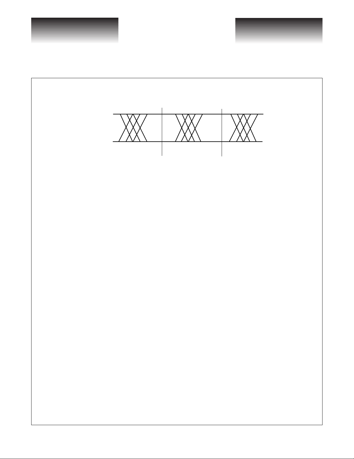
Figure 1: Retiming Offset
Advance Product Information
VSC8162
DI
Sampling point at the
center of the eye
PH_ADJ[4:0] = 00000
1:16 Demultiplexer
The demultiplexer inside of the VSC8162 consists of a 1:16 demultiplexer and timing circuitry which gen-
erates a divide-by-16 clock from the high speed clock input. The demultiplexer accepts a serial data stream
input (DI+/DI-) at 2.488 Gb/s and deserializes it into 16 parallel differential outputs (D0..D15). The timing
parameters of the parallel data outputs (D0..D15) are specified with respect to the falling edge of CLK16, so
that CLK16 can be used to clock the destination of D0..D15.
The parity output of the demultiplexer is the XOR of all 16 parallel outputs. The DINVERT input is an ECL
input (see Table 6) which can be used to invert the sense of the data through the demultiplexer. If DINVERT is
left floating, it defaults to the low state, which is the state that corresponds to normal operation (no data inversion).
Sampling point
delayed ~50ps from
the center of the eye
PH_ADJ[4:0] = 00100
FILTI, FILTO Pins
The FILTI and FILTO pins are used to provide additional capacitance to the loop filter of the VCO. To opti-
mize the VCO’s performance, it is recommended that 0.1
FILTI+ and FILTI- pins, as well as the FILTO+ and FILTO- pins.
Supplies
The VSC8161 is designed to operate with V
the part can be operated in an all positive supply environment, or a mixed positive and negative supply environment.
To operate in an all positive supply environment, each of the supply voltages must be shifted up by 5.2V
such that V
supply environment, each of the supply voltages must be shifted up by 2.0V such that V
V
= -3.2V and V
EE
Bear in mind that termination voltages must be adjusted to reflect any shift in supply voltages.
Page 4
will now be GND, V
EE
= +2.0V
CC
741 Calle Plano, Camarillo, CA 93012 • 805/388-3700 • FAX: 805/987-5896 9/14/98
.
= +3.2V and V
TT
VITESSE
SEMICONDUCTOR CORPORATION
= -5.2V, V
EE
F, size 0805 capacitors are connected between the
= -2.0V and V
TT
= +5.2V. To operate in a mixed positive and negative
CC
= GND (0.0V). However,
CC
will now be GND,
TT
G52209-0, Rev. 2.0
VITESSE
A
SEMICONDUCTOR CORPORATION
dvance Product Information
SC8162
2.488 Gbit/sec SONET/SDH
1:16 Demux with Clock Recovery
Interface Recommendations
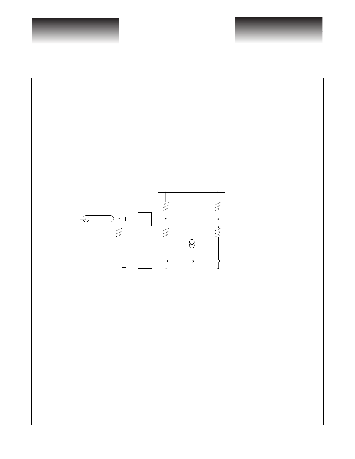
REFCK+, REFCK– Inputs
Internal biasing will position the reference voltage of approximately -1.32V on both the true and comple-
ment inputs. This input can either be DC coupled or AC coupled; it can also be driven single-ended or differentially. Figure 2 shows the configuration for single-ended, AC-coupling operation. In the case of direct coupling
and single-ended input, it is recommended that a stable V
input.
Figure 2: Single-ended AC Coupling for REFCK+, REFCK– Inputs
Chip Boundary
Z
O
C
IN
REFCK+
-1.32V
for ECL levels be used for the complementary
REF
= GND
V
CC
-1.32V
RT = Z
O
R
= 1kΩ (Approx.)
| |
V
TT
CIN TYP = 0.1µF
C
TYP = 0.1µF for single ended applications.
SE
V
C
TT
selected for REFCLK = 19.44 MHz)(Capacitor values are
SE
REFCK–
= -2V
V
TT
G52209-0, Rev. 2.0
9/14/98 741 Calle Plano, Camarillo, CA 93012 • 805/388-3700 • FAX: 805/987-5896
VITESSE
SEMICONDUCTOR CORPORATION
Page 5
VITESSE
SEMICONDUCTOR CORPORATION
Ω
2.488 Gbit/sec SONET/SDH
1:16 Demux with Clock Recovery
High Speed Data Input:
Advance Product Information
VSC8162
The data input receiver is internally terminated with a 100 ohm resistor between the true and complement
inputs. The inputs are internally biased to allow AC coupling. These inputs are recommended to be AC coupled
to permit use with a variety of limiting amplifiers. See Figure 3.
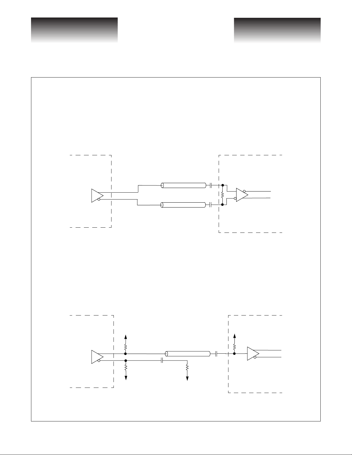
Figure 3: High-Speed Data Input Termination
8162Limiting Amp
Zo = 50Ω
= 50Ω
Z
o
0.1 µF
0.1 µF
DI
100Ω
DIN
High Speed Data Output:
A high speed data output termination scheme is shown in Figure 4. In order to disable the high speed data
switching, the 422
pulldown resistors can be removed.
Figure 4: High-Speed Data Output Termination
8162 Laser Driver
V
EE
V
422Ω
422Ω
EE
DO
DON
0.1 µF
Zo = 50Ω
50Ω
V
TERM
0.1 µF
V
TERM
50Ω
Page 6
VITESSE
741 Calle Plano, Camarillo, CA 93012 • 805/388-3700 • FAX: 805/987-5896 9/14/98
SEMICONDUCTOR CORPORATION
G52209-0, Rev. 2.0
 Loading...