

VITESSE VSC8151QV Datasheet
VITESSE
SEMICONDUCTOR CORPORATION
Advance Product Information
SC8151
STS-48/STM-16 Section Terminator
2.488Gb/s SONET/SDH
Features
• Integrated 2.488Gb/s T ransceiver
• SONET/SDH Transport Overhead Output
• SONET/SDH Transport Overhead Modification
• B1 Error Detection, Re-calculation, and Insertion
• Support for Multiple SONET/SDH Rates
• LOF/SEF Alarm Generation
• Section & Line AIS Insertion
• 50Ω Source Terminated 2.488Gb/s I/O
General Description
The VSC8151 is a 2.488Gb/s Section Termination device which both monitor s and modif ie s the secti on and
line overhead of a received SONET/SDH signal, and can generate AIS-L maintenance signals for trouble sectionalization. These features allow all section termination requirements to be supported for Operations, Administration, Management, and Provisioning (OAM&P) functions in SONET/SDH terminal and optical networking
applications. An integrated 2.488Gb/s serial transceiver isolates the SONET/SDH signal interface, allowing
protocol information to be exchanged with programmable logic using a low-speed TTL interface.
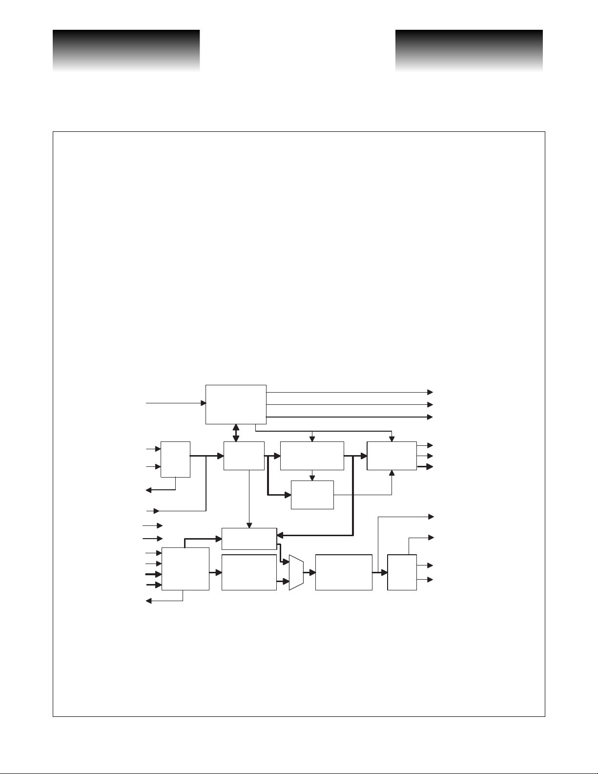
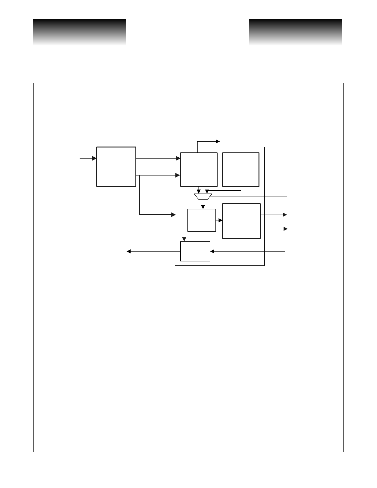
VSC8151 Functional Block Diagram
RXFRERR
RXSEF
RXLOF
RXFPOUT
RXOHCLK
RXOHOUT[7:0]
TXPOUT[15:0]
POUTCLK
TXSCLKOUT+/TXSOUT+/-
LOS
RXSIN+/-
RXSCLKIN+/-
POUTCLK
RXPIN[15:0]
SYSRST
TXSCLKIN+/-
TXOHWI
TXWRENA
TXADDR[5:0]
TXOHIN[7:0]
TXFPOUT
RXPIN[7:0]
1:8
DMX
OVERHEAD
INPUT &
INTERNAL
CONTROL
CONTROL
& ALARM
DETECTION
FRAMING
ASSEMBLER
AIS
GENERATION
DESCRAMBLER
B1
MONITOR
SCRAMBLER
& B1 CALC
OVERHEAD
OUTPUT
8:1
MUX
NOTE: References (R#-#) or (O#-#) refer to the SONET requirement or option specification listed in
Bellcore document GR-253 CORE Issue 2, Rev. 2, January 1999.
Functional Overview
The VSC8151 is divided into two logic sections, a monitoring section and a modification section, each
interfaced externally through both 2.5G b/s serial interfaces as well as 16-bit paralle l interfaces. Incoming
G52225-0, Rev. 2.9
12/1/99 741 Calle Plano, Camarillo, CA 93012 • 805/388-3700 • FAX: 805/987-5896
VITESSE SEMICONDUCTOR CORPORATION
Page 1
VITESSE
SEMICONDUCTOR CORPORATION
2.488Gb/s SONET/SDH
STS-48/STM-16 Sect ion Terminator
Advance Product Information
VSC8151
SONET/SDH data is demultiplexed, framed, descrambled, and the 27 bytes of the section and line overhead are
output. The BIP parity of the incoming signal is calcul at ed and co mpared with t he received B1 and B2 bytes for
calculating received parity errors. The byte aligned data, calculated B1/B2 parity, and frame boundary location
are then passed to the modification section where new overhead bytes are inserted. The modified data is
rescrambled, and B1/B2 parity rec alculated (if desired) pr ior to serialization and ou tput. An internal state
machine generates a section alarm inhibit signal (AIS) with user defined transport overhead that can be alternatively transmitted in place of the received signal.
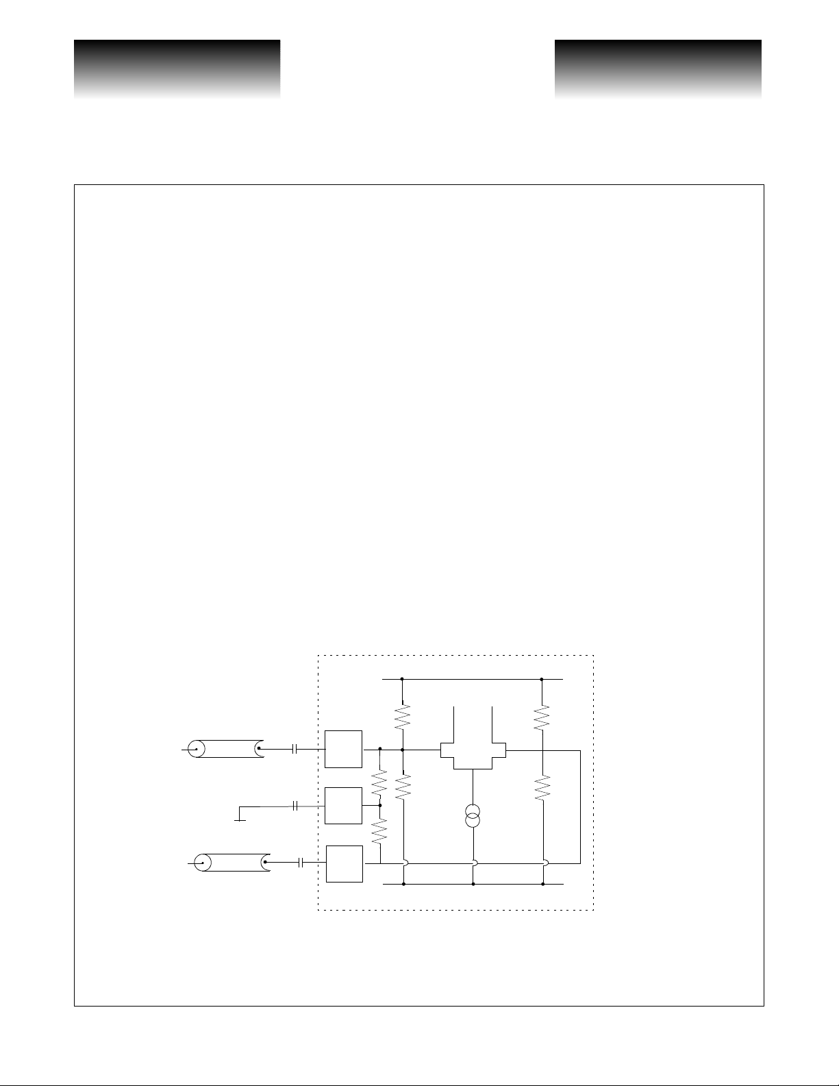
2.5G Serial and Parallel Input Interfaces
The demux receives differential clock and data signals at the appropriate SO NET/SDH rate and demu ltiplexes the data for framing. These inputs are interna lly terminated by a ce nter-tapped resistor network and
include biasing resistors to fa cil ita te AC coupling. For differential input DC coupling, the netw ork is t ermi nated
to the appropriate termination voltage V
providing a 50Ω to V
Term
inputs. For differential input AC coupling, the network is terminated to V
The common mode reference voltage is created by a resistor divider as shown. If the input signal is driven
differentially and DC-coupled to the part, the mid-point of the input signal swing should be centered about this
reference voltage and not e xceed the max imum al lo wa ble ampl itude. F or sing le-ended , DC-coupl ing o perations,
it is recommended that the user provides an external reference voltage which has better temperature and power
supply noise rejection than the on-chip resistor divider. The external reference should have a nominal value
equivalent to the common mode switch point of the DC coupled signal, and can be connected to either side of
the differential gate.
Figure 1: High Speed Serial Clock and Data Inputs
termination for both true and complement
Term
via a blocking capacitor.
Term
Z
O
C
V
TERM
Z
O
CIN TYP = 100 pF (clock), 100nF (data)
C
TYP = 100 pF (clock), 100nF (data) for single ended applications.
SE
Page 2
741 Calle Plano, Camarillo, CA 93012 • 805/388-3700 • FAX: 805/987-5896 12/1/99
Chip Boundary
V
= 3.3V
CC
C
IN
50Ω
AC
50Ω
C
SE
VITESSE SEMICONDUCTOR CORPORATION
1.65V 1.65V
V
= 0V
EE
R
= 1.5k
Ω
| |
G52225-0, Rev. 2.9
VITESSE
SEMICONDUCTOR CORPORATION
Advance Product Information
SC8151
STS-48/STM-16 Section Terminator
2.488Gb/s SONET/SDH
The serial demux can be bypassed and the 16-bi t single-ended PECL bu s R XPIN[1 5: 0] can be used to input
SONET/SDH data for applications where the data has already been deserialized by a previous device. This
mode is selected by asserting the EQULOOP input (active high). Input setup and hold requirements are specified with respect to t he f a lli ng edg e of POUTCLK; th e user is responsible for meeting loop timi ng requirement s
between the VSC8151 and previous device. The user must still provide a line rate clock to the serial clock input
RXSLKIN+/- to provide a high-speed output clock to the mux and the means to create the divide-by-16 POUTCLK.
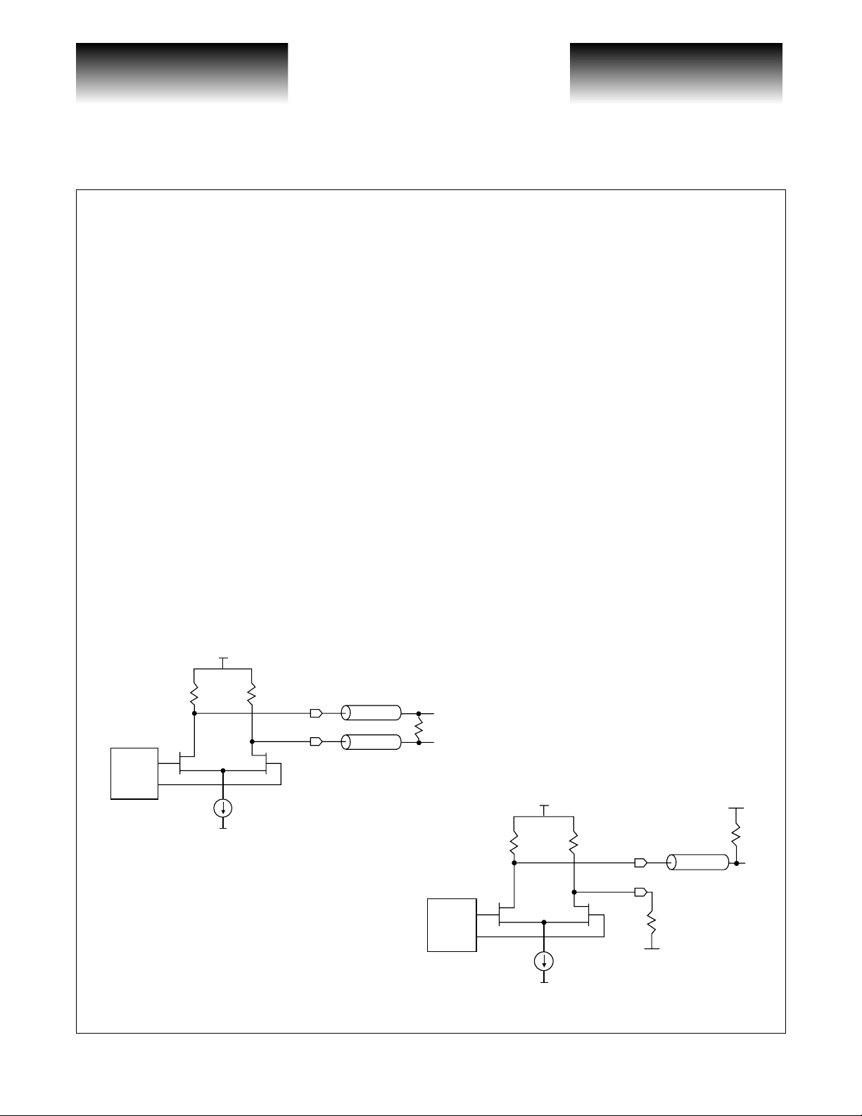
2.5G Serial and Parallel Output Interfaces
The high speed clock and data outp ut driver consists of a differential pair design ed to drive a 50Ω transmission line. The transmission line should be terminated with a 100Ω resistor at the load between true and complement outputs. No connection to a termination voltage is required. The output driver is source terminated to 50
on-chip, providing a snubbing of any reflections. If used single-ended, one way to terminate the output driver is
differentially at the load with a 100Ω resistor between true and com plement outpu ts. See Figure 2 A. Another
option is to terminate the used output at the load with 50 ohm to V
V
at the source. See Figure 2B.
TERM
In some applications, it may be desirable to turn off the high speed outputs (TXSOUT, TXSCLKOUT) to
reduce power. To disable the high speed clock output, tie pin 22 to V
high speed data output, t i e pi n 1 7 t o V
(3.3V) instead of GND. T urning off each output will reduce maximum
CC
current consumption by 107mA for the clock output, and 122mA for the data output.
and the unused output with 50 ohm to
TERM
(3.3V) instead of GND. To disable the
CC
Ω
Figure 2A
Pre-Driver
50Ω
Figure 2: High Speed Output Driver & Termination
V
CC
50Ω
100Ω
Z0 = 50Ω
Figure 2B
V
EE
Pre-Driver
50Ω
V
CC
50Ω
50Ω
V
TERM
V
EE
Z0 = 50Ω
50Ω
V
TERM
G52225-0, Rev. 2.9
12/1/99 741 Calle Plano, Camarillo, CA 93012 • 805/388-3700 • FAX: 805/987-5896
VITESSE SEMICONDUCTOR CORPORATION
Page 3
VITESSE
SEMICONDUCTOR CORPORATION
2.488Gb/s SONET/SDH
STS-48/STM-16 Sect ion Terminator
Advance Product Information
VSC8151
The serial mux output can be bypassed and the 16-bit single-ended PECL bus TXPOUT[15:0] can be used
to output modified SONET/S DH data or AIS to anoth er device. These outputs are enabled by setting the DP bit
in the MISC register app ropr i ately, and should be disabled if not being used. It i s possi ble to use both the 16-bit
parallel output bus and the 2.5Gb/s serial out put si multaneou sly. The POUTCLK output is used to provide a b us
output clock for RXFPOUT and is a divide-by-16 version of TXSCLKIN.
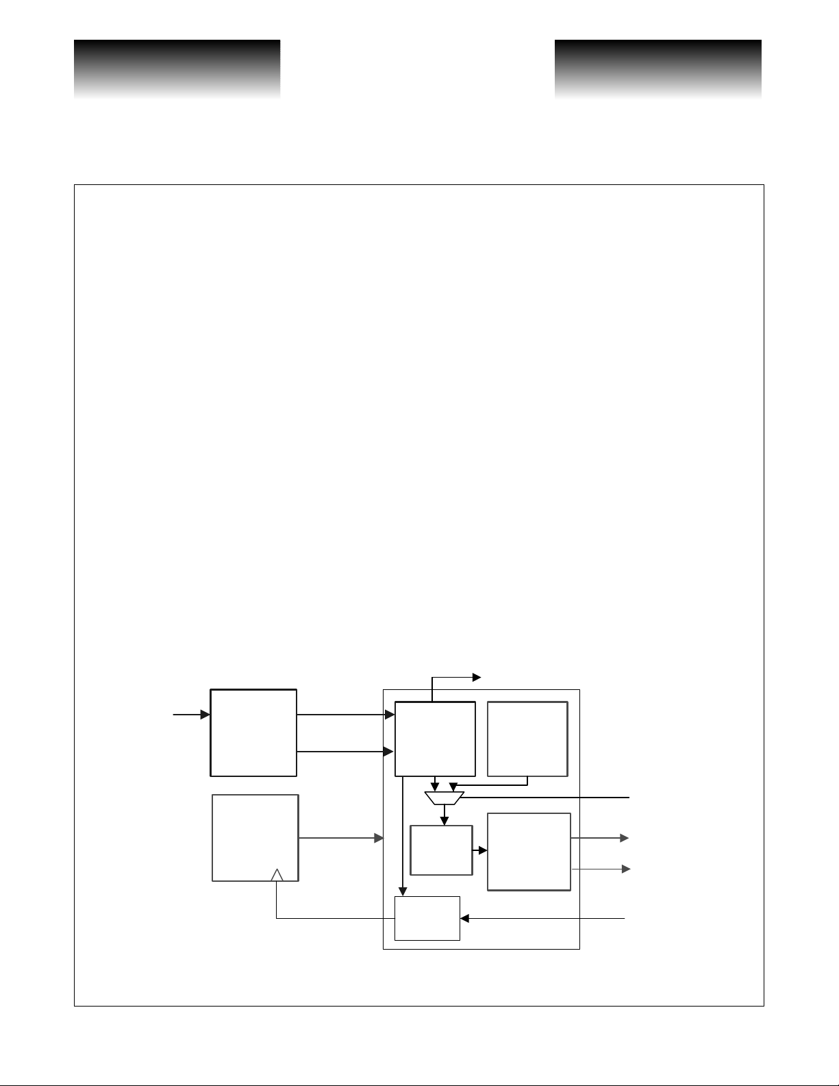
2.5G Output Clocking Domains
The 2.5GHz clock input to the VSC8151 mux (TXSCLKIN) acts as the pe rmanent transmit clock for the
VSC8151. An internal clock domain boundary exists between the monitor and the transmit sections of the
device, allowing the AIS transm it portio n to func tion co mpletely indepen dently of the rece ive portion. This
allows a CDR to track whatever data is being received and allows the VSC8151 to monitor in-frame status of
the signal continuously.
During a LOS condition, the CDR clock output may drift outside of the SONET/SDH transmission standard of +/-20PPM. By providing the option of using an external clock multiplication unit (CMU), one can
maintain a standard of +/-20PPM even during AIS states. This backup CMU rece ives it’s timing reference from
either a local AIS refer ence or the divided clock from the received RXSCLKIN +/- , depending whethe r AIS
transmit mode is selected or not.
The user controls the source of the reference clock ou tput through settings in the VS C8151 register file.
The user will change these settings at the same time AIS is asserted or when imminent loss of RXSCLKIN
clock quality exists. The AIS reference output can be switched from a divided down RXSCLKIN signal to a
copy of one of the external references, ensuring that a proper reference clock remains for the transmit multiplexer. (See Table 2: VSC8151 Configuration Registers, Definition 13)
Figure 3: VSC8151 using CMU as Transmit Timing Source
Received
Data
Clock and
Data Recovery
VSC8122
Clock
Multiplication
Unit
VSC812X
Page 4
741 Calle Plano, Camarillo, CA 93012 • 805/388-3700 • FAX: 805/987-5896 12/1/99
RXSIN+/-
2.488Gb/s Data
622Mb/s Data
155MB/s Data
2.488GHz Clock
622MHz Clock
155MHz Clock
RXSCLKIN+/-
TXSCLKIN+/-
2.488GHz Clock
622MHz Clock
155MHz Clock
SEF/LOF ALARMS
Demux &
Monitor
Logic
Modify
Logic
AIS State
Machine
Mux &
Frame
Assembly
Logic
AIS Reference
78 MHz
VITESSE SEMICONDUCTOR CORPORATION
CMU
Reference
Generator
AIS Insert
TXSOUT+/-
TXSCLKOUT+/-
AIS Reference
155/78 MHz
G52225-0, Rev. 2.9
VITESSE
SEMICONDUCTOR CORPORATION
Advance Product Information
SC8151
STS-48/STM-16 Section Terminator
2.488Gb/s SONET/SDH
If the user chooses to use the CDR as a t iming so ur ce even during AIS mode , the output of the CDR can be
connected single ended to both RXSCLK IN and TXSCLKIN, or a mult i-drop conn ection can b e made d if feren tially.
Figure 4: VSC8151 using CDR as Transmit Timing Source
SEF/LOF ALARMS
Demux &
Monitor
Logic
Modify
Logic
AIS State
Machine
Mux &
Frame
Assembly
AIS Insert
TXSOUT+/-
TXSCLKOUT+/-
Received
Data
Clock and
Data Recovery
VSC8122
RXSIN+/-
2.488Gb/s Data
622Mb/s Data
155MB/s Data
2.488GHz Clock
622MHz Clock
155MHz Clock
RXSCLKIN+/-
TXSCLKIN+/-
2.488GHz Clock
622MHz Clock
155MHz Clock
Logic
AIS Reference
78 MHz
CMU
Reference
Generator
AIS Reference
155/78 MHz
SONET/SDH Monitoring Circuitry Overview
The monitoring circuitry provides SONET/SDH compliant framing and framing alarms, as well as detect-
ing B1 and B2 parity errors and transport overhead byte output.
Framing
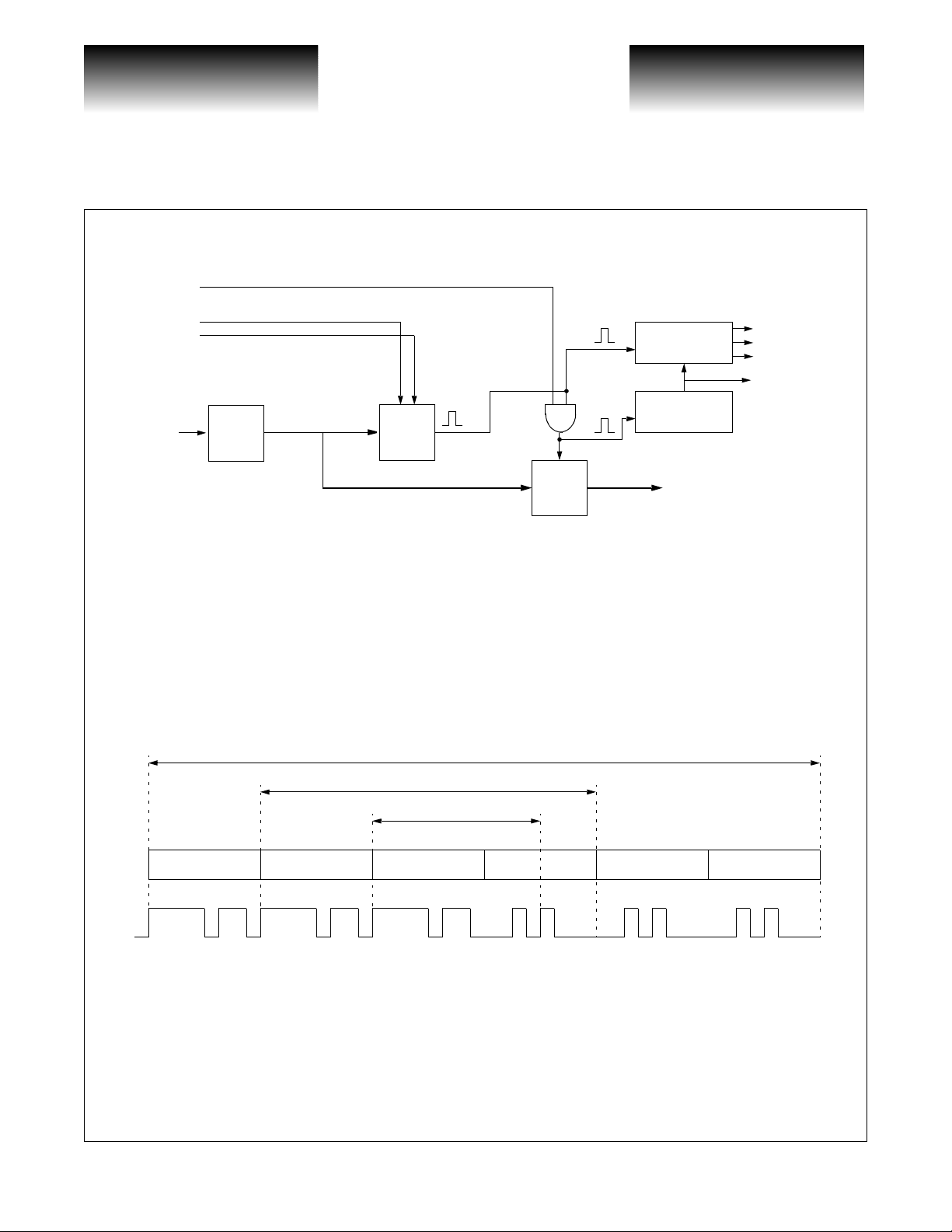
The frame acquisition algorithm determines the in-frame/out-of-frame status of the receiver. Out-of-frame
is defined as a sta te where th e frame boundaries of t he received SONET/SDH signal a re unkno wn, i .e. after sy s-
tem reset or if for some reason the receiver looses synchronizat i on, e.g. due to ‘bit sli ps’. In-frame is def ined as
a state where the frame boundaries are known.
The receiver monitors the frame synchronization by checking for the pres ence of a portion of the A1/A2
framing pattern every 125uS. If one or more bit errors are detected in the expected A1/A2 framing pattern output RXFRERR (active high) will be asserted (See Figure 5). If framing pattern errors are detected for four consecutive frames a Severely Errored Frame (SEF) alarm will be asserted on output RXSEF (active high) (R5-
223).
G52225-0, Rev. 2.9
12/1/99 741 Calle Plano, Camarillo, CA 93012 • 805/388-3700 • FAX: 805/987-5896
VITESSE SEMICONDUCTOR CORPORATION
Page 5
VITESSE
SEMICONDUCTOR CORPORATION
2.488Gb/s SONET/SDH
STS-48/STM-16 Sect ion Terminator
Figure 5: Functional Block Diagram of Frame Acquisition Circuit
FRD
SL1
SL0
RXSIN
1:8
DMX
FRAME
DET
Advance Product Information
VSC8151
RXFRERR
RXSEF
RXLOF
RXFPOUT
RESYNC
BYTE
ALIGN
ERROR/ALARM
DETECTION
FRAME SYNC.
COUNTER
Aligned Output
The frame boundary detection/verification is based on 12, 24 or 48 bits of the A1/A2 overhead (See
Figure 6) depending on the setting of the FRDET register (See Table 2). Frame acquisition procedures are controlled by the settings of the FRDET register. Reframing can be controlled manually or reframing can automatically be initiated by the presence of an SEF signal. Using SEF as an indicator that reframe is necessary will
achieve realignment within 250uS or the receipt of two error free framing patterns (R5-225)
A frame detect based on 24 bits will result in an SEF alarm at an av era ge of no more than once e v ery 6 minutes assuming a BER of 10-3 (R5-224). A frame detect based on 48 bits or 12 bits will result in a mean time
between SEF detects of 0.43 minutes and 103 minutes respectively.
Figure 6: Frame Detection Patterns
48 bits
24 bits
12 bits
A1 (0xF6) A1 (0xF6) A1 (0xF6) A2 (0x28) A2 (0x28) A2 (0x28)
Loss of Signal
The LOS (Loss of Signal, active high) input should be asserted whenever the interfacing module no longer
generates a valid electrical signal on the high speed clock and/or data lines of the VSC8151. If the clock signal
is present when the LOS input is a sserted th e VSC8151 wil l asser t SEF and ot her o utputs wil l become invalid. If
the input clock is not present, then the tr ansi ti on of t he LOS i npu t wil l not be dete cted and the part is effect ively
frozen. Asserting LO S will for ce SEF ( Severely Errored Frame) and L OF (Loss of Fram e) high, an d force all
0’s to be output from the device, regardless of the input.
Page 6
741 Calle Plano, Camarillo, CA 93012 • 805/388-3700 • FAX: 805/987-5896 12/1/99
VITESSE SEMICONDUCTOR CORPORATION
G52225-0, Rev. 2.9

VITESSE
SEMICONDUCTOR CORPORATION
Advance Product Information
SC8151
Loss of Frame
A Loss of Frame (LOF) defect is declared (RXLOF active h igh) when a Se ve rely Errored F rame (SEF) condition persists for 3ms (R6 -5 9). The LOF state detec tion is based on an integrating tim er to prevent sporadic
errors from asserting LOF, such as a periodic 1ms error. An LOF defect is cancelled after an in-frame condition
(SEF low) persists for 3ms (R6-61) because an integrating timer approach has been implemented (O6-62).
Multiple SONET/SDH Rate Functionality
The VSC8151 supports three SONET/SDH rates: STS-48/STM-16, STS-12/STM-4, and STS-3/STM-1.
The user is responsible for rate-provisioning the device by setting the RATESEL register (See Table 2). The
device requires clocks RXSCLKIN+/- and TXSCLKIN+/- to match the selecte d data rate in order for internal
circuitry to function correctly. The RATESEL register changes the expected frame length of the received signal
and selects the characteristics of the outgo in g traffic or AIS signal. LOF in tegration timing remains 3ms reg ardless of selected SONET/SDH rate.
Descrambler
Framed SONET/SDH bytes are descrambled using a frame synchron ous descr ambl er wit h generat i ng pol ynomial 1 + X6 + X7 and a sequence length of 127. The scrambling algorithm is reset to an all 1’s state immediately following the Z0 byte (last channel of first row, third column). The A1, A2, and J0/Z0 bytes are not
descrambled (R5-6). The descrambler can be disabled by setting the MISC register appropriately.
STS-48/STM-16 Section Terminator
2.488Gb/s SONET/SDH
B1 Error Monitoring
The bit-interleaved parity (BIP-8) error detection code (B1) will be calculated for every received frame
before descrambling and compared to the descrambled B1 value in the following frame (R3-16). The results of
this calculation are used to generate a B1 parit y mask that is ou tput using th e ov erhead output interf ace. The calculated B1 parity used to do this com parison c an be sub stituted in the re ceived data stream and ou tput. This
effectively ‘corrects’ the B1 byte and prevents the same B1 errors from being detected downstream.
B2 Error Monitoring
Incoming B2 errors for the first STS-1 are monitored and detected. This circuitry is not designed to supply
B2 error rate monitoring but exists to provide support for modification of the overhead bytes of the line overhead. Incoming B2 pa rity must be dete rmined bec ause modification of the line overhead require s that the B2
byte for the first STS-1 be re-calculated. If the line overhead is not being modified by the user then the B2 error
monitoring still takes place and the B2 errormask is output.
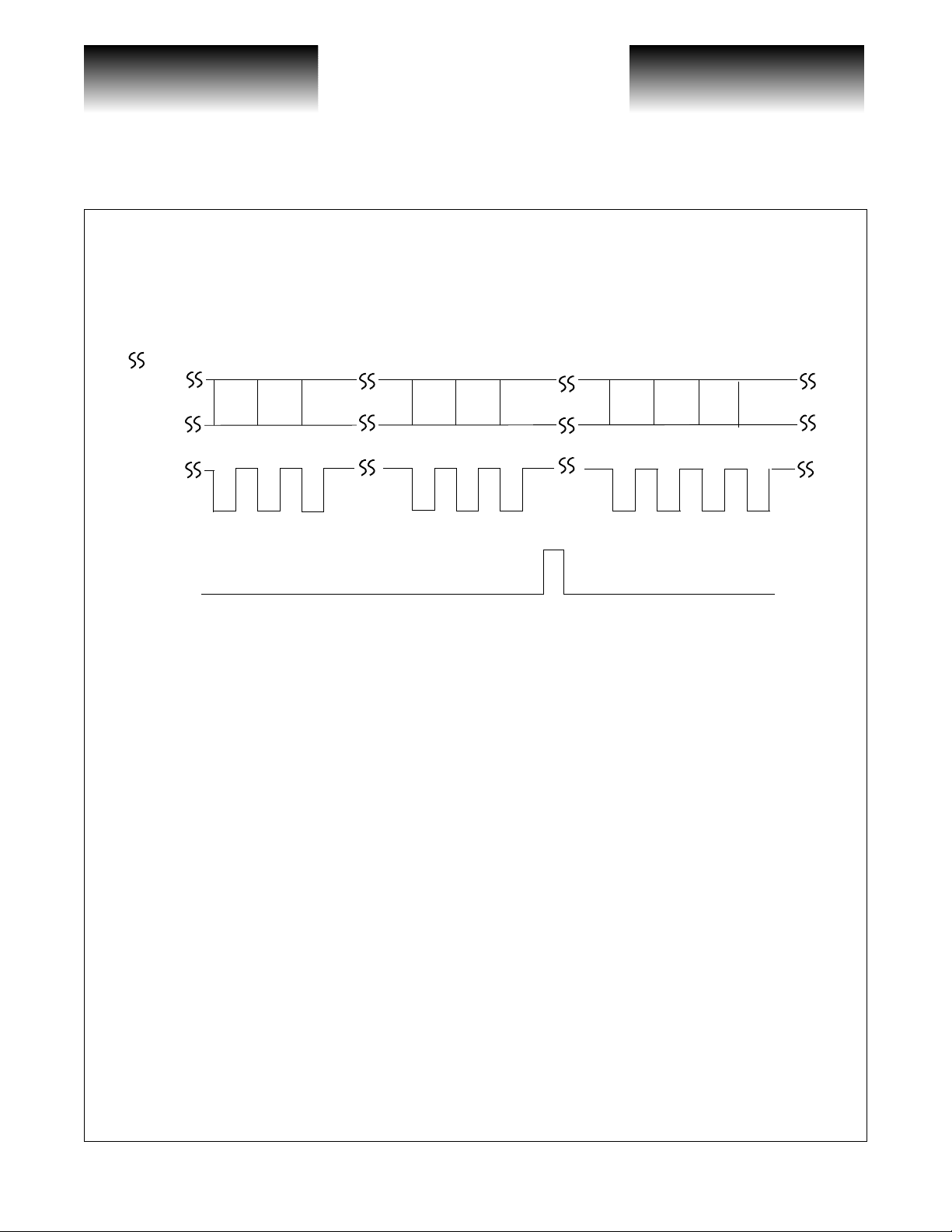
Overhead Output
The 9 bytes of the SONET section overhead and the 18 bytes in the first channel of the line overhead (See
Figure 7) are made available to the user through the overhead output inter face RXOHOU T[7:0], RXOH CLK,
and RXFPOUT. Two additional bytes containing the r esul ts of the B1 and B2 parity error detect i on are also output. These 29 bytes are output from the RXOHOUT port, each accompanied by a pulse of RXOHCLK. The 27
overhead bytes are output in the order they are received, with a pulse on RXFPOUT appearing after the J0 byte.
RXFPOUT is used to provide a reference point for the 29 byte output sequ ence of overhead bytes and clocks
G52225-0, Rev. 2.9
12/1/99 741 Calle Plano, Camarillo, CA 93012 • 805/388-3700 • FAX: 805/987-5896
VITESSE SEMICONDUCTOR CORPORATION
Page 7
VITESSE
R
SEMICONDUCTOR CORPORATION
2.488Gb/s SONET/SDH
STS-48/STM-16 Sect ion Terminator
(See Figure 7). It is suggested that RXOHCLK be used to clock an external counter with RXFPOUT providing
a counter reset. This allows the counter value to be correlated to a specific output byte and to be used as a write
address for a register file.
Figure 7: Functional Overhead Output Timing
= delay
RXOHOUT[7:0]
XOHCLK
RXFPOUT
M0 E2 A1 A2 J0 B1 E1 F1
S1
Advance Product Information
VSC8151
B1MASK
The additional two bytes are parity error masks that indicate the number of received B1 and B2 errors.
These bytes contain a parity error-mask of the results of the BIP calculation. Incoming parity errors are desig-
nated by a ‘1’ in the correspon din g bi t posi tio n. A B1 or B2 error mask byte of 00H indicates no received parity
errors for that frame, and a byte of 13H would indicate 3 of 8 bits were errored. The B1 error mask appears
immediately after the F1 user byte is output and the B2 error mask appears immediately after the K2 APS byte
is output.
The RXOHOUT[7:0] output is undefined when SEF is high. RXFPOUT and RXOHCLK are functions of
the received data being properly framed and will also be indeterminate during a SEF or LOS condition.
SONET/SDH Modification Circuitry Overview
The modification circuitry receives frame aligned data from the monitoring circuitry or from an internal
state machine that generates a section AIS signal. The transp ort o verhe ad of either signal can be modif ied b y the
user, including the insertion of recalculated B1 parity. These features encompass the requirements for performing section termination, as well as allowing the modification of line overhead bytes such as K1/K2 and the line
DCC bytes.
Overhead Write Interface
The 9 bytes of the sect ion o v erhead a nd the 18 b ytes of t he f irst c hanne l of th e line overhead can be repla ced
with user defined bytes or allowed to pass through the part unchanged. The overhead write interface makes use
of an internal 32 byte register file for storing the 27 overhead modifier bytes as well as providing internal configuration registers. TXWRENA, TXADDR[5:0], TXOHWI, and TXOHIN[7:0] are the write interface inputs.
Page 8
741 Calle Plano, Camarillo, CA 93012 • 805/388-3700 • FAX: 805/987-5896 12/1/99
VITESSE SEMICONDUCTOR CORPORATION
G52225-0, Rev. 2.9

VITESSE
SEMICONDUCTOR CORPORATION
Advance Product Information
SC8151
Data present on the TXOHIN[7:0] bus is written to the internal register addressed by TXADDR[5:0] on the rising edge of TXWRENA. Assertion of TXOHWI (active high) during the overhead byte write cycle inhibits the
modification of the addressed overhead byte.
A1/A2 Boundary Modification
Only the first A1 and A2 bytes of the SONET/SDH can be modif ied. The A1 by te can be replaced with user
defined data without affecting the framing algorithms of subsequent VSC8151 devices. An F6H byte can be resubstituted before exiting the subsequent VSC8151, effectively creating an in-band 64kb/s messaging channel.
The A2 byte could be replaced by t he user to inte ntion ally corrup t the A1/A2 bou ndary and outpu t a data stream
that causes downstream network equipment to lose frame lock and enter alarm states.
BIP-8 Recalculation & Modification
The TXOHIN[7:0] information written to the B1 and B2 add ress loc ation does n ot replace t he outg oing BIP
byte. The 8 bits form an XOR mask that will intentionally induce BIP e rrors into the outgoing data stream. A
TXOHIN[7:0] word such a s B2H would co rrupt the BIP byte at bits 1 , 4, 5, 7, and a d ownstream device will
observe four parity errors. A TXOHIN[7:0] word of 00H will induce no parity errors, but will replace the BIP
byte with a recalculated value. Setting the TXOHWI bit at the B1 or B2 location will prevent the BIP byte from
being modified or corrected.
Note that if there is any modif icati on to the transport ov erhead it is necessary for th e B1 byte to be corrected
in order to prevent downstream parity errors. The B2 byte needs to be corrected if any changes are made to the
line overhead for the same reason.
Errors can be intentionally induced to the B2 channel to compensate for the lack of complete B2 error monitoring. Modifying the line overhead requires that the B2 byte in the first STS-1 be corrected, but this has the
effect of artificially lowering the observed B2 error rate at subsequent line termination equipment (LTE). Correcting the B2 byte i n the f ir st STS- 1 position will resul t in a 1 /48th , 1/12t h, or 1/3r d reduc tion dependin g on the
provisioned SONET/SDH rate. Monitoring received B2 errors on the RXOHOUT[7:0] B2 errormask and rewriting this errormask to the B2 address will keep the outgoing B2 error rate consistent with the received B2
error rate.
STS-48/STM-16 Section Terminator
2.488Gb/s SONET/SDH
Alarm Indication Signal (AIS) Overhead Modification
Transport overhead modification procedures are identical for AIS transmiss ion mode. TXFPOUT is
sourced from the frame counters resident within the receive framing circuitry during non-AIS transmiss ion
mode. During an AIS condition valid SONET/SDH data is no longer being received, resulting in the part entering a LOF or LOS state. Counters in the receive framing block will be invalid during this time, therefore when
AIS is asserted the TXFPOUT signal is sourced from a redundant set of frame counters present within the AIS
generation state machine. The frame counters for AIS block are separate from the receiv e framing circuitry, and
as a result the TXFP OUT signal wi ll be in an unknown state durin g a AIS mo de transition , but will become
periodic again after 125us. User logic should anticipate a late or early TXFPOUT pulse when switching in and
out of AIS mode.
G52225-0, Rev. 2.9
12/1/99 741 Calle Plano, Camarillo, CA 93012 • 805/388-3700 • FAX: 805/987-5896
VITESSE SEMICONDUCTOR CORPORATION
Page 9
 Loading...