

VITESSE VSC8150QQ Datasheet
VITESSE
SEMICONDUCTOR CORPORATION
Preliminary Data Sheet
SC8150
2.488Gb/s SONET/SDH
Overhead Monitor
Features
• Integrated 2.488 Gb/s Demultiplexer
• Outputs SONET/SDH Transport Overhead
• Support for Multiple SONET/SDH Rates
• B1 Calculation and Error Reporting
• LOF/SEF Alarm Generation
• Serial Data Loopthrough Output
• 100 PQFP Package
• Single 3.3V Supply Option
General Description
The VSC8150 monitors an SONET/SDH signal in order to provide section and line data for Operations,
Administration, Maintenance, and Provisioning (OAM&P) at multiple SONET/SDH rates. Differential PECL
clock and data input receivers and a differential data output isolate the high-speed interface. Low-speed TTL
inputs and outputs allow the use of inexpensive programmable logic to perform OAM&P functions. The
VSC8150 is an ideal solution for constructing a non-intrusive SONET/SDH monitoring interface when visibility of payload data is not required.
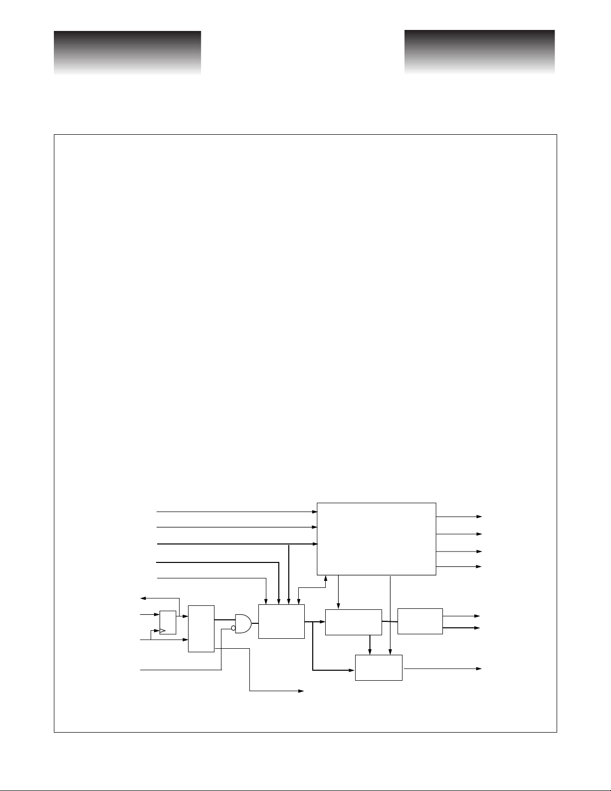
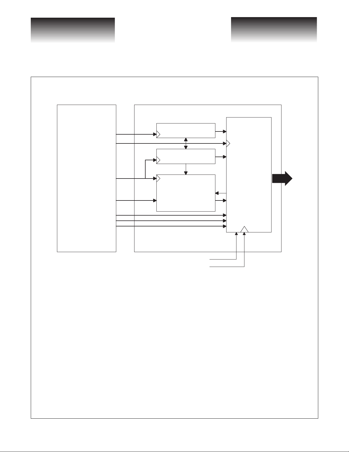
Functional Description
The VSC8150 high-speed interface receives recovered SONET/SDH data RXSIN +/− and clock RXSCLKIN
framing alarms generated. Incoming B1 parity is calculated and compared with the transmitted B1 value, and
detected errors are output. The 27 bytes of the first STS-1 transport overhead are descrambled and output for
processing.
+/− and provides a re-timed data output RXSLBOUT +/− . Internally the data is framed and SEF/LOF
VSC8150 Functional Block Diagram
DISDSCRM
RESET
RATESEL[1:0]
SELFRDET[1:0]
FRDETEN
RXSLBOUT+/-
RXSIN+/-
RXSCLKIN+/-
LOS
G52186-0, Rev. 3.0
10/12/98 741 Calle Plano, Camarillo, CA 93012 • 805/388-3700 • FAX: 805/987-5896
1:8
DMX
RXPIN[7:0]
VITESSE
FRAMER
RXPCLKIN
SEMICONDUCTOR CORPORATION
DESCRAMBLER
311MHz INTERNAL
CLOCK SOURCE
CONTROL
&
ALARM DETECTION
OVERHEAD
LATCH
B1 CHECK
RXFPOUT
RXFRERR
RXSEF
RXLOF
SOHCLK
SOHOUT[7:0]
B1ERR
Page 1
VITESSE
SEMICONDUCTOR CORPORATION
2.488Gb/s SONET/SDH
Preliminary Data Sheet
Overhead Monitor
NOTE: References (R#-#) or (O#-#) refer to the SONET requirement or option specification listed in
Bellcore document GR-253 CORE Issue 2.
Framing
The frame acquisition algorithm determines the in-frame/out-of-frame status of the receiver. Out-of-frame
is defined as a state where the frame boundaries of the received SONET/SDH signal are unknown, i.e. after system reset or if for some reason the receiver loses synchronization, e.g. due to ‘bit slips’. In-frame is defined as a
state where the frame boundaries are known.
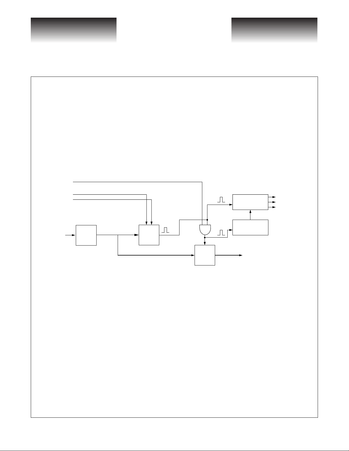
Figure 1: Functional Block Diagram of Frame Acquisition Circuit
FRDETEN
SEFFRDET1
SELFRDET0
ERROR/ALARM
DETECTION
VSC8150
RXFRERR
RXSEF
RXLOF
FRAME SYNC.
RXSIN
The receiver monitors the frame synchronization by checking for the presence of a portion of the A1/A2
framing pattern every 125uS. If one or more bit errors are detected in the expected A1/A2 framing pattern
RXFRERR will be asserted for 51.44ns. If framing pattern errors are detected for four consecutive frames a
Severely Errored Frame (SEF) alarm will be asserted (RXSEF active high) ( R5-206 ) (See Figure 7and 10).
The frame boundary detection/verification is based on 12, 24 or 48 bits of the A1/A2 overhead (See Figure
2) depending on the setting of the SELFRDET input (See Table 1). Frame acquisition is initiated when the
FRDETEN input is held high. This control is level sensitive and the VSC8150 will continually perform frame
acquisition as long as FRDETEN is held high; a suggested implementation is to short FRDETEN logically or
physically to the SEF output. Such an arrangement will achieve realignment within 250uS or the receipt of two
error free framing patterns (
A frame detect based on 24 bits will result in an SEF alarm at an average of no more than once ev ery 6 minutes assuming a BER of 10-3 (
between SEF detects of 0.43 minutes and 103 minutes respectively.
1:8
DMX
R5-208 ).
R5-207 ). A frame detect based on 12 bits or 48 bits will result in a mean time
FRAME
DET
RESYNC
BYTE
ALIGN
OUT
COUNTER
Page 2
VITESSE
741 Calle Plano, Camarillo, CA 93012 • 805/388-3700 • FAX: 805/987-5896 10/12/98
SEMICONDUCTOR CORPORATION
G52186-0, Rev. 3.0
VITESSE
SEMICONDUCTOR CORPORATION
Preliminary Data Sheet
SC8150
Table 1: Frame Detection Select Settings
Function
24 bits 1 0
48 bits 0 1
12 bits 0 0
Frame detection disabled 1 1
A1 (0xF6) A1 (0xF6) A1 (0xF6) A2 (0x28) A2 (0x28) A2 (0x28)
2.488Gb/s SONET/SDH
Overhead Monitor
SELFRDET1 SELFRDET0
Figure 2: Frame Detection Patterns
48 bits
24 bits
12 bits
Loss of Signal
A Loss of Signal (LOS active high) input is provided to prevent noise from propagating into the overhead
output logic. Logic zeros will be clocked into the device when LOS is active high, and SEF will be immediately
synchronously asserted, with LOF appearing 3ms afterward. If RXSCLKIN+/- disappears before LOS is
asserted the part will freeze and SEF/LOF will never appear.
Loss of Frame
A Loss of Frame (LOF) defect is declared (RXLOF active high) when a Severely Errored Frame (SEF)
condition persists for 3ms (
errors from not asserting LOF, such as a periodic 1ms error. In the event of sporadic errors, the out of frame
timer increments when RXSEF = 1. It is on hold when RXSEF = 0 and does not change state as long as this
condition lasts for < 3 ms. The out of frame timer is reset to it’s initial state if the RXSEF is low for > 3 ms, and
an LOF defect is cancelled after an in-frame condition (RXSEF low) persists for a total of 3ms (
Multiple SONET/SDH Rate Functionality
The VSC8150 supports three SONET/SDH rates: STS-48/STM-16, STS-12/STM-4, and STS-3/STM-1.
The user is responsible for rate-provisioning the device by setting the two inputs RATESEL[1:0] (See Table 2).
The device requires a clock rate appropriate to the selected data rate in order for internal circuitry to function
correctly. LOF integration timing is 3ms regardless of the rate selected.
R6-59 ). The LOF state detection is based on an integrating timer to prevent sporadic
R6-61 ).
G52186-0, Rev. 3.0
10/12/98 741 Calle Plano, Camarillo, CA 93012 • 805/388-3700 • FAX: 805/987-5896
VITESSE
SEMICONDUCTOR CORPORATION
Page 3
VITESSE
SEMICONDUCTOR CORPORATION
2.488Gb/s SONET/SDH
Preliminary Data Sheet
Overhead Monitor
Table 2: SONET/SDH Rate Select Settings
Function
STS-3/STM-1 0 1
STS-12/STM-4 1 0
STS-48/STM-16 0 0
Invalid 1 1
RATESEL1 RATESEL0
Descrambler
Framed SONET/SDH bytes are descrambled using a frame synchronous descrambler with generating polynomial 1 + X6 + X7 and a sequence length of 127. The scrambling algorithm is reset to an all 1's state immediately following the Z0 byte ((SONET 192 x 3) | (SDH 64x9) = 577th received byte in frame). All A1, A2, and
J0/Z0 bytes are not descrambled (
R5-6 ).
B1 Error Monitoring
The section bit-interleaved parity (BIP-8) error detection code B1 will be calculated for every frame before
de-scrambling and compared to its extracted value after de-scrambling the B1 value in the following frame (R3-
16). If B1 errors were detected in the previous frame a series of pulses will appear on the B1ERR output, beginning approximately 60ns after the B1 byte is received. The number of pulses indicates the quantity of errored
bit positions detected; the absence of pulses indicates no received B1 errors, and eight pulses would indicate the
maximum number of received B1 errors. The pulses are eight parallel clocks wide (25.7nS at 2.488GHz RXSCLKIN), and spaced apart by the same amount (See figure 10).
VSC8150
Overhead Byte Read Out
Overhead bytes are descrambled (with the exception of A1, A2, and J0) and output from SOHOUT[7:0] in
the order of their appearance in the frame. Only the bytes from the first STS-1 frame or the first, fourth, and
seventh columns of the first STM-1 frame are presented (See Figure 6). Accompanying the data from the
SOHOUT[7:0] output are the output clock SOHCLK and frame pulse RXFPOUT (See Figures 8 and 9).
The SOHOUT output is undefined when SEF is high. The user should be aware that overhead data from
one frame prior to the RXFRERR pulse could be corrupted and should not be used for OAM&P functions.
FPGA Interface
RXFPOUT is used to provide a reference point to the 27 byte sequence of overhead bytes and clocks. It is
suggested that the SOHCLK be used to clock an external counter with RXFPOUT used as the counter reset.
The count value can be used as the overhead byte address, and RXPOUT will reset the counter when it reaches
a logical value of 27. The high order bit of this counter is useful for indicating when the B1 pulse train results
can be read. A block diagram illustrates this arrangement more clearly. (See Figure 3).
Page 4
741 Calle Plano, Camarillo, CA 93012 • 805/388-3700 • FAX: 805/987-5896 10/12/98
VITESSE
SEMICONDUCTOR CORPORATION
G52186-0, Rev. 3.0
VITESSE
SEMICONDUCTOR CORPORATION
Preliminary Data Sheet
SC8150
Figure 3: Suggested VSC8150 System Implementation
VSC8150
B1ERR
RXFPOUT
SOHCLK
SOHOUT[7:0]
RXSEF
RXLOF
RXFRERR
FPGA
4 Bit Counter
RESET
RESET
5 Bit Counter
WA[4:0]
D[7:0] Q[7:0]
27x8 Register File
Q[2:0]
Q4
RA[4:0]
2.488Gb/s SONET/SDH
Overhead Monitor
OAM&P
B1 Count
Frame Count
B1 V alid
OH Data
LOS
System Clock
High Speed Interface
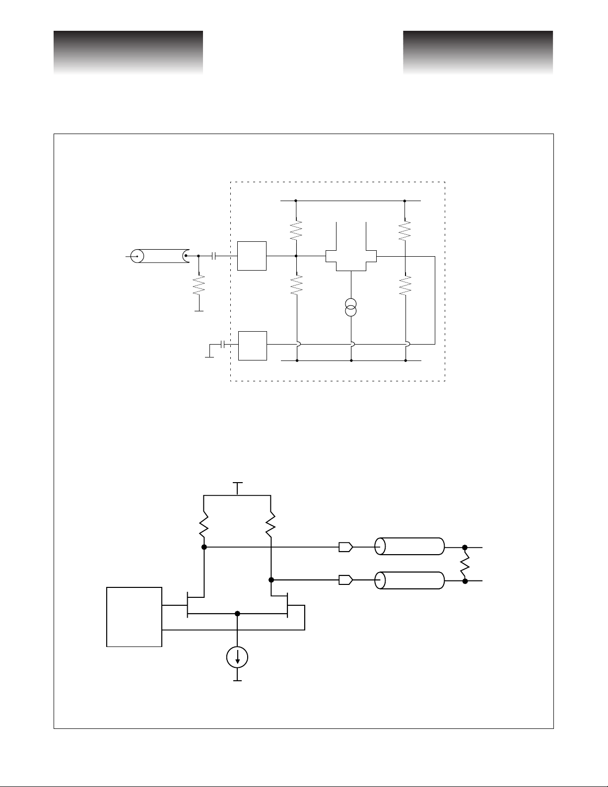
Serial data received on the RXSIN+/- inputs is retimed on the falling edge of RXSCLKIN+/- clock and
appears on the serial loopback output RXSLBOUT+/- (See Figure 11). This interface will pass data at all frequencies from DC to 2.5GHz, and does not necessarily have to retime SONET/SDH data.
Inputs RXSIN+/- and RXSCLKIN+/- do not have internal termination resistors, but internal biasing resistors provide a bias voltage suitable for AC coupling (See Figure 4).
In most situations these inputs will have high transition density and little DC offset. However, in cases
where this does not hold, direct DC connection is possible. All serial data and clock inputs have the same circuit topology, as shown in figure 4.
signal is driven dif ferentially and DC-coupled to the part, the mid-point of the input signal swing should be centered about this reference voltage and not exceed the maximum allowable amplitude. For single-ended, DCcoupling operations, it is recommended that the user provides an external reference voltage which has better
temperature and power supply noise rejection than the on-chip resistor divider. The external reference should
have a nominal value equivalent to the common mode switch point of the DC coupled signal, and can be connected to either side of the differential gate.
The reference voltage is created by a resistor divider as shown. If the input
G52186-0, Rev. 3.0
10/12/98 741 Calle Plano, Camarillo, CA 93012 • 805/388-3700 • FAX: 805/987-5896
VITESSE
SEMICONDUCTOR CORPORATION
Page 5
VITESSE
SEMICONDUCTOR CORPORATION
2.488Gb/s SONET/SDH
Overhead Monitor
Z
O
RT = Z
Preliminary Data Sheet
Figure 4: High Speed Serial Clock and Data Inputs
Chip Boundary
VCC = 3.3V
C
IN
O
V
Term
C
SE
V
EE
1.65V
1.65V
= 0V
V
EE
VSC8150
= 1.5kΩ
R
| |
CIN TYP = 100 pF
CSE TYP = 100 pF for single ended applications. (Capacitor values
are selected for DI = 2.5Gb/s.)
Figure 5: High Speed Output Termination
V
CC
50Ω
50Ω
Pre-Driver
100Ω
Z0 = 50Ω
Page 6
V
EE
VITESSE
741 Calle Plano, Camarillo, CA 93012 • 805/388-3700 • FAX: 805/987-5896 10/12/98
SEMICONDUCTOR CORPORATION
G52186-0, Rev. 3.0
 Loading...