VITESSE VSC8140TW, VSC8140QR Datasheet
VITESSE
SEMICONDUCTOR CORPORATION
Data Sheet
SC8140
Transceiver with Integrated Clock Generator
2.48832Gb/s 16:1 SONET/SDH
Features
• 2.48832Gb/s 16-Bit Transceiver
• Targeted for SONET OC-48 / SDH STM-16
Applications
• LVPECL Low-Speed Interface
• On-chip PLL-Based Clock Generator
• High-Speed Clock Output With Power-Down
Option
• Supports Parity at the 16-Bit Parallel T ransmit
and Receive Interfaces
• Provides Equ ipment, Facilities an d Split Loopback Modes as well as Loop Timing Modes
• Loss of Signal (LOS) Detect input
• Meets Bellcore Jitter Performance Specifications
• Single +3.3V Supply
• 2.25 Watts Typical Power Dissipation
• Packages: 128-pin PQFP or 208-pin TBGA
General Description
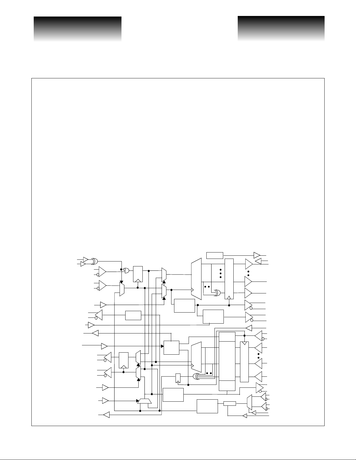
The VSC8140 is a SONET/SDH compatible transceiver with integrated clock generator for use in SONET/
SDH systems operating at a 2.48832Gb/s data rate. The internal clock generator uses a Phase-Locked Loop
(PLL) to multiply either a 77.76MHz or 155.5 2MHz ref er ence cl ock in ord er to provi de t he 2.488 32GHz clo ck
for internal logic and output retiming. The 16-bit parallel interface incorporates an on-board FIFO eliminating
loop timing design issues by providing a flexible parallel timing a rchitecture. In addition, the dev ice provides
both facility and equipment loopback modes and two loop timing modes. The VSC8140 operates using a 3.3V
power supply, and is available in either a th ermally-enh anced 128-PQF P or a thermally- enhanced 208 -pin
TBGA package.
VSC8140 Block Diagram
LOS
POL
RXIN+
RXIN-
RXCLKIN+
RXCLKIN-
EQULOOP
CLK128O+
CLK128O-
RXCLKO_FREQSEL
OVERFLOW
FIFORESET
TXOUT+
TXOUT-
TXCLKOUT+
TXCLKOUT-
FACLOOP
LOOPTIM0
PARERR
Q D
Divide
by 128
D Q
Divide by
FIFO
CNTRL
Divide by
16
16
voltage
Divide by
2
2.48832GHz
PLL
gen.
Output Register
Write
Pointer
16x5 FIFO
Read
Pointer
VREFOUT
VREFIN
RXOUT0
RXOUT15
RXPARITYOUT
RXCLK16O+
RXCLK16O-
RXCLKO16_32+
RXCLKO16_32-
PARMODE
TXCLK16I+
TXCLK16I-
TXIN0
TXIN15
Input Register
TXPARITYIN
TXCLK16O+
TXCLK16O-
LPTIMCLK+
LPTIMCLK-
REFCLK+
REFCLK-
LOOPTIM1
REF_FREQSEL
G52251-0, Rev. 4.0
VITESSE SEMICONDUCTOR CORPORATION
9/6/00 741 Calle Plano, Camarillo, CA 93012 • 805/388-3700 • FAX: 805/987-5896
Page 1
VITESSE
SEMICONDUCTOR CORPORATION
2.48832Gb/s 16:1 SONET/SDH
Transceiver with Integrated Clock Generator
Data Sheet
VSC8140
Functional Description
Transmitter Low-Speed Interface
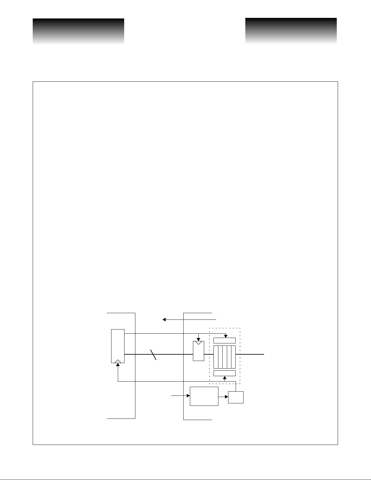
The Upstream Device should use the TXCLK16O as the timing source for its final output latch (see Figure
1). The Upstream Device should then generate a TXCLK16I that is phase-aligned with the data. The VSC8140
will latch TXIN[15:0]
respect to TXCLK16I (see Table 1).
A FIFO exists within the VS C8140 to eliminate difficult system loop timing issues. O nce the PLL has
locked to the reference clock, RESET must be held low for a minimum of five CLK16 c ycles to initialize the
FIFO, then RESET should be set high and held constant for continuous FI FO operation. For the transpar ent
mode of operation (no FIFO), simply hold RESET at a constant low state (see Figure 2).
The use of a FIFO permits the system designer to tolerate an arbitrary amount of delay between
TXCLK16O and TXCLK16I. Once RESET is asserted and the FIFO initialized, the delay between TXCLK16O
and TXCLK16I can decrease or increase up to one period of th e low-spee d clock (6.4ns). Should this delay dri ft
exceed one period, the write pointer and the read pointer could point to the same word in the FIFO, resulting in
a loss of transmit ted d ata ( a F IFO o verf low ). In the e ven t of a FIF O ove rfl ow, an active low OV ERFLO W signal is asserted (for a minimum of five TXCLK16I cycles) which can be used to initiate a reset signal from an
external controller.
The TXCLK16O
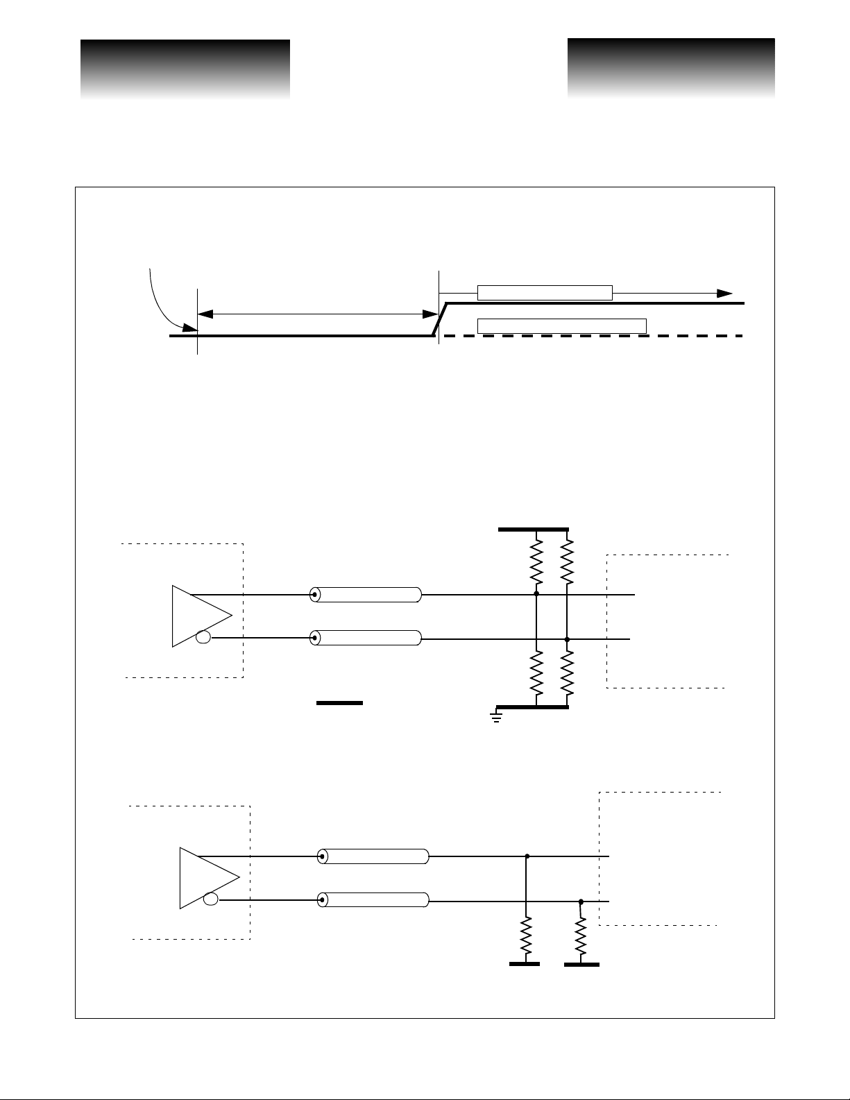
transmission line can be DC termin ated wit h a spli t-end t erminat ion scheme (see F igure 3), or DC terminat ed by
50Ω to V
substituted for the traditional 50Ω to V
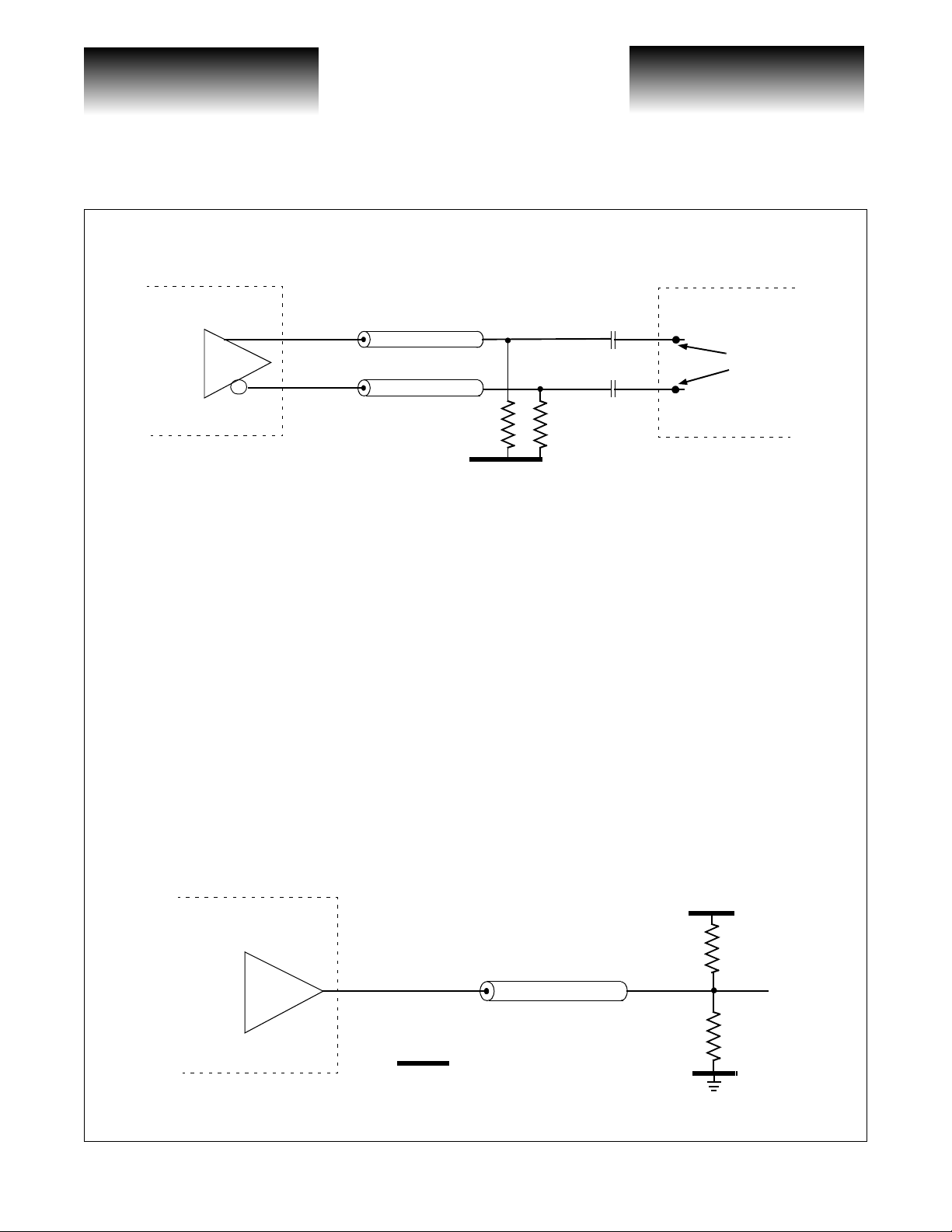
ods. Figure 5 illustrates an AC-coupling met hod for the occasi on when the downstr eam device provid es the bias
point for AC-coupling.
-2V on each line (see Figure 4). At any time, the equivalent split-end termination technique can be
CC
± on the rising edge of TXCLK16I+. The data must meet setu p and hold times with
± output driver is a LVPECL output driver designed to drive a 50
-2V on each line. AC-coupling can be ac hieved by a number of meth-
CC
transmission line. The
Ω
Page 2
741 Calle Plano, Camarillo, CA 93012 • 805/388-3700 • FAX: 805/987-5896 9/6/00
Figure 1: Low-Speed Systems Interface
OVERFLOW
TXCLK16I
16
TXCLK16O
REFCLK
VITESSE SEMICONDUCTOR CORPORATION
2.48832GHz
VSC8140
PLL
16 x 5 FIFO
write
read
Div 16
G52251-0, Rev. 4.0
VITESSE
SEMICONDUCTOR CORPORATION
Data Sheet
SC8140
Transceiver with Integrated Clock Generator
Figure 2: Enabling FIFO Operation
2.48832Gb/s 16:1 SONET/SDH
PLL locked to reference clock.
Minimum 5 CLK16 cycles
RESET
Holding RESET “low” for a minimum of 5 CLK16 cycles, then setting “high” enables FIFO operation.
Holding RESET constantly “low” bypasses the FIFO for transparent mode operation.
Figure 3: DC Termination of Low-Speed LVPECL RXCLK16O, RXCLK16_32O, TXCLK16O Outputs
VSC8140
Split-end equivalent termination is ZO to V
R1 = 125Ω R2 = 83Ω, ZO=50Ω, V
Z
o
TERM
TERM
= VCC-2V
FIFO Mode Operation
Transparen t M o de Operation
V
CC
R1
R1
downstream
Z
o
R1||R2 = Z
VCCR2 + VEER1
Figure 4: DC Termination of Low-Speed LVPECL RXCLK16O, RXCLK16_32O, TXCLK16O Outputs
R1+R2
O
= V
TERM
V
EE
R2
R2
downstream
VSC8140
G52251-0, Rev. 4.0
9/6/00 741 Calle Plano, Camarillo, CA 93012 • 805/388-3700 • FAX: 805/987-5896
VITESSE SEMICONDUCTOR CORPORATION
Z
o
R1 =50Ω
VCC-2V
R1 =50Ω
VCC-2V
Page 3
VITESSE
SEMICONDUCTOR CORPORATION
2.48832Gb/s 16:1 SONET/SDH
Transceiver with Integrated Clock Generator
Figure 5: AC Termination of Low-Speed LVPECL RXCLK16O, RXCLK16_32O, TXCLK16O Outputs
VSC8140
Z
o
100nF
downstream
Data Sheet
VSC8140
bias point
generated
internally
Receiver Low-Speed Interface
Z
o
100nF
50Ω
50Ω
V
CC
-2V
The demultiplexed serial stream is made available by a 16-bit single-ended LVPECL interface
RXOUT[15:0] with accompanying differential LVPECL divide-by-16 clock RXCLK16O
LVPECL divide-by-16 or -32 clock RXCLK16_32O
RXCLKO_FREQSEL is used to select RXCLK16_32O
RXCLK16_32O
± output as 77.76MHz, RXCLKO_FREQSEL = “1” designates RXCLK16_32O± output as
±.
±. RXCLKO_FREQSEL = “0” designates
± and selectable
155.52MHz.
The RXCLK16O and RXCLK1 6_32O outp ut drivers ar e designe d to drive a 5 0Ω transmission line. The
transmission line can be DC termin ated wit h a spli t-end t erminat ion scheme (see F igure 3), or DC terminat ed by
50Ω to V
-2V on each line (see Figure 4). A C-coupling can be achieved by a number of m ethods. Figure 5
CC
illustrates an AC-coupling method for the occasion when the downstream device provides the bias point for
AC-coupling. The divide-by-16 output (RXCLK16O) or the divide-by-16 or -32 output (RXCLK16_32O) can
be used to provide an external looptiming reference clock (after external filtering with a 1x REFCLK PLL) for
the clock multiplication unit on the VSC8140.
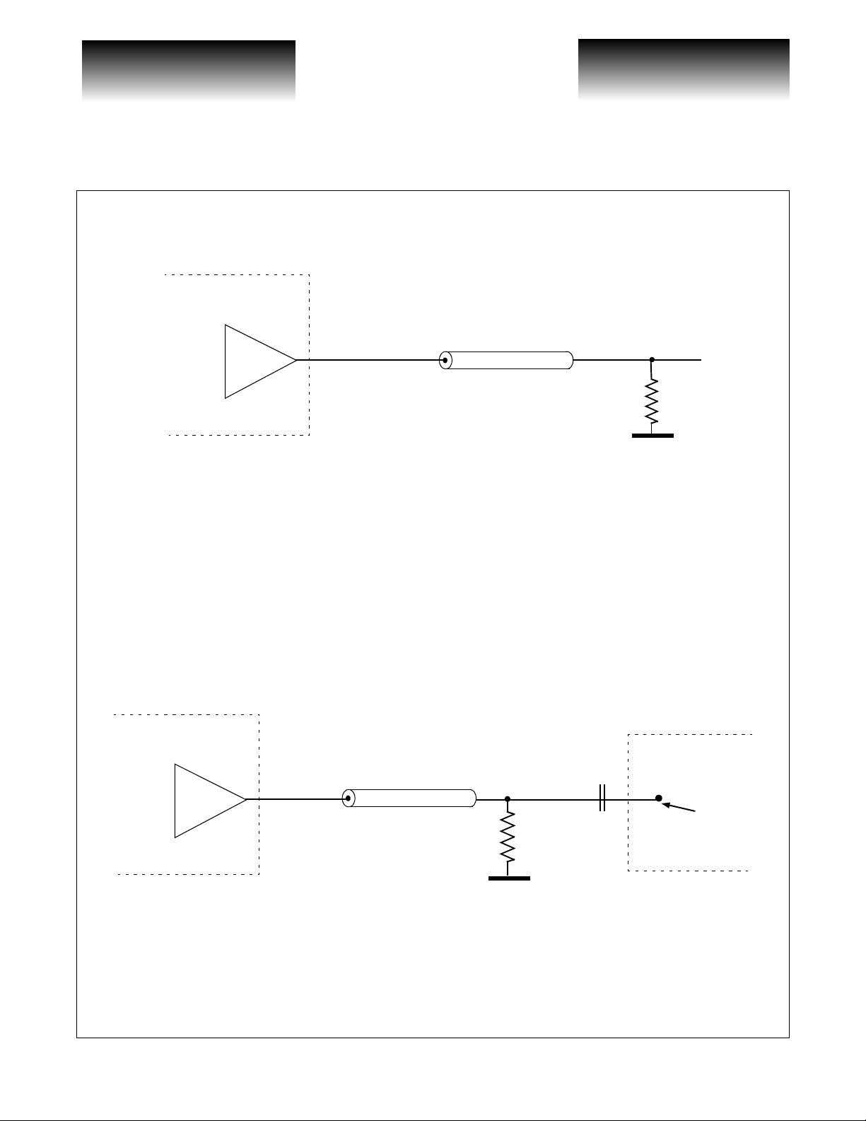
The RXOUT[15:0] output drivers are designed to drive a 50Ω transmission line which can be DC terminated with a split-end termination scheme (see Figure 6), or a traditional termination scheme (see Figure 7).
Figure 6: Split-end DC Termination of Low-Speed LVPECL RXOUT[15:0] Outputs
VSC8140
Page 4
741 Calle Plano, Camarillo, CA 93012 • 805/388-3700 • FAX: 805/987-5896 9/6/00
Split-end equivalent termination is ZO to V
R1 = 125Ω R2 = 83Ω, ZO=50Ω, V
R1||R2 = Z
V
CC
VITESSE SEMICONDUCTOR CORPORATION
o
R2 + VEER1
R1+R2
= V
TERM
TERM
Z
TERM
= VCC-2V
R1 = 125Ω
o
V
CC
R2 = 83Ω
V
EE
G52251-0, Rev. 4.0
VITESSE
SEMICONDUCTOR CORPORATION
Data Sheet
SC8140
Figure 7: Traditional DC Termination of Low-Speed LVPECL RXOUT[15:0] Outputs
Transceiver with Integrated Clock Generator
2.48832Gb/s 16:1 SONET/SDH
VSC8140
Z
o
R1 =50Ω
VCC-2V
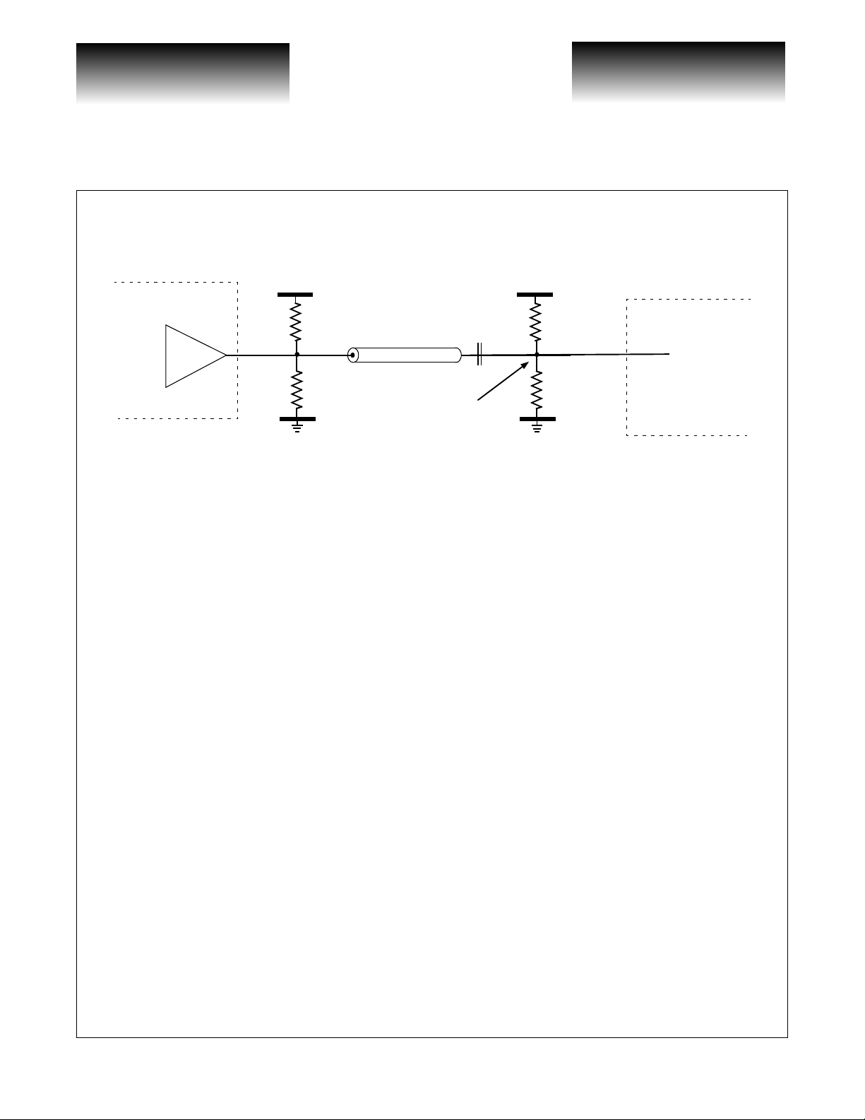
The RXOUT[15:0] outp ut drivers ca n also be ap propriate ly AC-co upled by a number of m ethods, ho wever, DC-coupling is preferred since there is no guarantee of transition density for individual bits in the 16-bit
word. Figure 8 illustrates an AC-coupling method for the occasion when the downs tream device pro vides the
bias point for AC-coupling. Figure 9 illustrates an AC-coupling method for the occasion when the bias point
needs to be generated externally. The resistor values in Figure 9 were selected to generate a bias point of 1.98V,
the mid-point for LVPECL V
generate the necessary bias point for the downstream device.
and VOL as specified for the VSC8140. Resistor values should be selected to
OH
Figure 8: AC Termination of Low-Speed LVPECL RXOUT[15:0] Outputs
VSC8140
Z
o
100nF
R1 = 50Ω
VCC-2V
G52251-0, Rev. 4.0
9/6/00 741 Calle Plano, Camarillo, CA 93012 • 805/388-3700 • FAX: 805/987-5896
VITESSE SEMICONDUCTOR CORPORATION
downstream
bias point
generated
internally
Page 5
VITESSE
SEMICONDUCTOR CORPORATION
2.48832Gb/s 16:1 SONET/SDH
Transceiver with Integrated Clock Generator
Figure 9: AC Termination of Low-Speed LVPECL RXOUT[15:0] Outputs
V
CC
V
CC
Data Sheet
VSC8140
VSC8140
R1 = 125Ω
Z
o
100nF
R2 = 83Ω
bias point
V
EE
Parity
Systems employing internal parity are supported by the VSC8140. On the transmit side, a parity check is
performed between the TXPARITYIN input and the 16 TXIN[15:0] bits.
PARM ODE is use d to selec t even or odd parity expected for these 17 b its. (TXIN[ 15:0] an d TXPARI-
TYIN). PARMODE = “0” selects odd, PARMODE = “1” selects even. The PARERR output (parity error output) is asserted active high when the parity of the 17 bits (TXIN[15:0] and TXPARITYIN) does not conform to
the expected parity designated by PARMODE. PARERR becomes available T
TXCLK16I. PARERR is a NRZ pulse that is updated every 6.4 ns, i.e., the period of TXCLK16I. The timing
relationship of PARERR to TXCLK16I is shown in Figure 17. The PARERR pin may be left open if parity is
unused.
On the receive side, the parity output (RXPARITYOUT) is simply the XOR of all 16 outputs.
generated
externally
V
EE
R3 =83Ω
R4 = 125Ω
DV
downstream
after the rising edge of
Loss of Signal
The VSC8140 has a TTL input LOS to force the part into a Loss of Signal (LOS) state. Most optics have a
TTL output usually called Signal Detect (SD), based on the optical power of the incoming light stream.
Depending on the optics manufacturer, this signal is either active high or low. To accommodate polarity differences, the internal Loss of Sign al is generated when the POL and LOS i nputs a re of o pposit e states. Once acti ve,
all zeroes “0” will be propagated downstream u sing the transmit clock until the optical signal is regained and
LOS and POL are in the same logic state.
Page 6
741 Calle Plano, Camarillo, CA 93012 • 805/388-3700 • FAX: 805/987-5896 9/6/00
VITESSE SEMICONDUCTOR CORPORATION
G52251-0, Rev. 4.0
VITESSE
SEMICONDUCTOR CORPORATION
Data Sheet
SC8140
Transceiver with Integrated Clock Generator
2.48832Gb/s 16:1 SONET/SDH
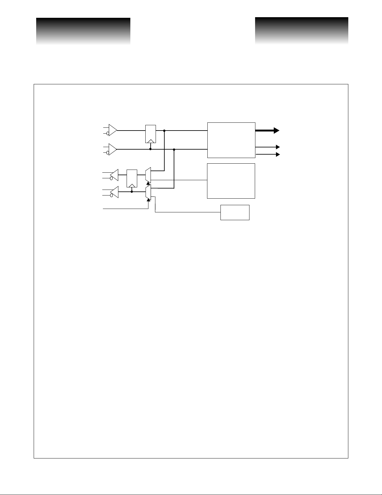
Figure 10: Facility Loopback Data Path
RXIN+
RXIN-
RXCLKIN+
RXCLKIN-
TXOUT+
TXOUT-
TXCLKOUT+
TXCLKOUT-
FACLOOP
Q D
D Q
1
0
1
0
1:16 Serial to
Parallel
16:1 Parallel to
Serial
2.48832GHz
PLL
RXOUT[15:0]
RXCLK16O
RXCLK32O
Facility Loopback
The facility loopback function is controlled by the FACLOOP signal. When the FACLOOP signal is set
high, the Facility Loopback mode is activated and the high-speed serial receive data (RXIN) is presented at the
high-speed transmit output (TXOUT), as depicted in Figure 10. In addition, the high-speed receive clock input
(RXCLKI) is selected and presented at the high-speed transmit clock output (TXCLKOUT). In Facility Loopback mode, the high-speed receive data (RXI N) is also convert ed to paral lel data and pr esented at the low-sp eed
receive output pins (RXOUT[15:0]). The receive clock (RXCLKIN) is also divided down and presented at the
low-speed clock output (RXCLK16O).
Equipment Loopback Data Path
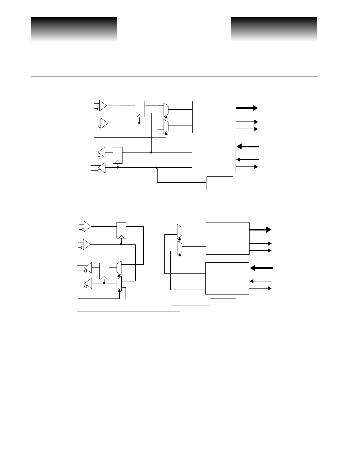
The Equipment Loopback function is controlled by the EQULOOP signal, which is active high. When the
Equipment Loopback mode is activated, the high-speed transmit data generated from the parallel to serial conversion of the low-speed data (TXIN[15:0]) is selected and converted back to parallel data in the receiver section and presented at the low-speed parallel data outputs (RXOUT[15:0]), as shown in Figure 11. The internally
generated OC-48 clock is used to generate the low-speed receive output clocks (RXCLK16O and
RXCLK16_32O). In Equipment Loopback mode, the transmit data (TXIN[15:0]) is serialized and presented at
the high-speed output (TXOUT) along with the high-speed transmit clock (TXCLKOUT) which is generate d by
the on-chip PLL.
G52251-0, Rev. 4.0
9/6/00 741 Calle Plano, Camarillo, CA 93012 • 805/388-3700 • FAX: 805/987-5896
VITESSE SEMICONDUCTOR CORPORATION
Page 7
VITESSE
SEMICONDUCTOR CORPORATION
2.48832Gb/s 16:1 SONET/SDH
Transceiver with Integrated Clock Generator
Figure 11: Equipment Loopback Data Path
EQULOOP
TXCLKOUT+
TXCLKOUT-
RXIN+
RXIN-
RXCLKIN+
RXCLKIN-
RXIN+
RXIN-
RXCLKIN+
RXCLKIN-
TXOUT+
TXOUT-
Q D
D Q
D Q
Figure 12: Split Loopback Datapaths
Data Sheet
VSC8140
0
1
0
1
0
1
0
1
1:16 Serial to
Parallel
16:1 Parallel to
Serial
2.48832GHz
PLL
1:16 Serial to
Parallel
RXOUT[15:0]
RXCLK16O
RXCLK32O
TXIN[15:0]
TXCLK16I
TXCLK16O
RXOUT[15:0]
RXCLK16O
RXCLK32O
TXOUT+
TXOUT-
TXCLKOUT+
TXCLKOUT-
FACLOOP
EQULOOP
Q D
1
0
1
0
16:1 Parallel to
Serial
2.48832GHz
PLL
TXIN[15:0]
TXCLK16I
TXCLK16O
Split Loopback
Equipment and Facility Loop back modes can b e enabled simultaneou sly. In this case, high-speed serial data
received (RXIN) and clock (RXCLKIN) are muxed through to the high-speed serial outputs (TXOUT and
TXCLKOUT). The low-speed 16-bit transmit stream (TXIN[15:0]) is muxed into the low-speed 16-bit receive
output stream (RXOUT[15:0]). See Figure 12.
Looptiming
LOOPTIM0 mode bypasses the PLL when LOOPTIM0 is asserted high. In this mod e, the PL L is by passed
using the receive high-speed clock (RXCLKIN), and the entire part is synchronously clocked from a single
external source.
Page 8
741 Calle Plano, Camarillo, CA 93012 • 805/388-3700 • FAX: 805/987-5896 9/6/00
VITESSE SEMICONDUCTOR CORPORATION
G52251-0, Rev. 4.0
VITESSE
SEMICONDUCTOR CORPORATION
Data Sheet
SC8140
When LOOPTIM1 is asserted high, the RXCLK16_32O or RXCLK16O output can be tied to the LPTIMCLK input. In order to meet jitter transfer, the RXCLK16_32O or RXCLOCK16O needs to be filtered by a 1X
PLL circuit with a narrow pass characteristic. The part is forced out of this m ode in Equipment Loo pback to
prevent the PLL from feeding its own clock back.
Clock Generator
An on-chip PLL generates the 2 .48832GHz transmit c lock from the ex ternally provided REF CLK input.
The on-chip PLL uses a low phase noise reactance-based Voltage Controlled Oscillator (VCO) with an on-chip
loop filter (with two external 0.1µF peaking ca pacito rs). Th e loop ban dwi dth of th e PL L is wi thin t he SO NET
specified limit of 2MHz.
The customer can select to pr ovide either a 77. 76MHz reference, or 2x of that refer ence, 155.52MHz.
REF_FREQSEL is used to select the desired reference frequency. REF_FREQSEL = “0” designates REFCLK
input as 77.76MHz, REF_FREQSEL = “1” designates REFCLK input as 155.52MHz.
The REFCLK should be of high quality since noise on the REFCLK below the loop bandwidth of the PLL
will pass through the PLL and appear as jitter on the output. Preconditioning of the REFCLK signal with a
VCXO may be required to avoid passing REFCLK noise with greater than 2ps RMS of jitter to the output. The
VSC8140 will output the REFC LK noise in addit ion to the intrinsic jitter from the VSC 8140 itse lf during such
conditions.
Transceiver with Integrated Clock Generator
2.48832Gb/s 16:1 SONET/SDH
Loop Filter
The PLL on the VSC8140 employs a n inte rnal lo op fi lter wit h of f -chip pea kin g capaci tors. The PL L desi gn
is fully differential, therefore the loop filter must also be fully differential. One capacitor should be connected
between FILTAO and FILTAI, with the other connected between FILTAON and FILTAIN. Recommended
capacitors are low-inductance 0.1µF 0603 ceramic SMT X7R devices with a voltage rating equal to or greater
than 10V.
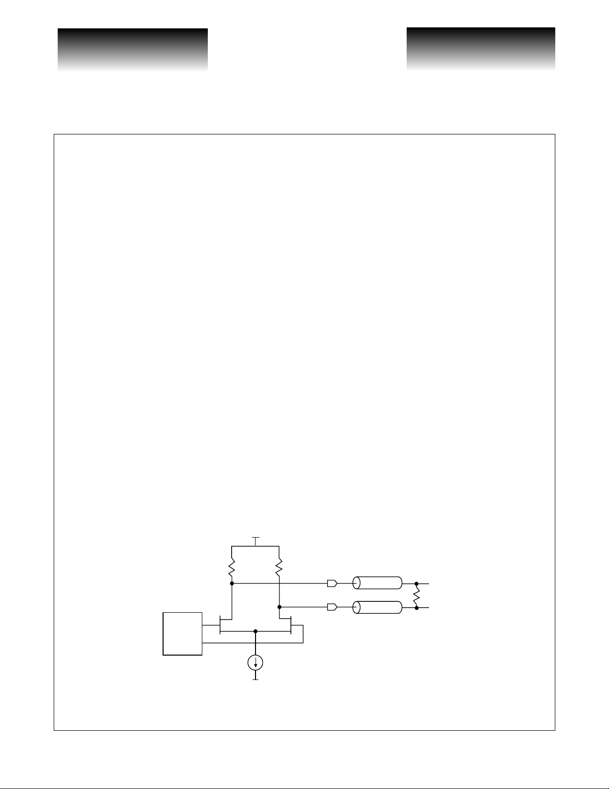
Figure 13: High-Speed Output Termination
V
CC
50Ω
100Ω
Z0 = 50Ω
Pre-Driver
50Ω
V
EE
G52251-0, Rev. 4.0
9/6/00 741 Calle Plano, Camarillo, CA 93012 • 805/388-3700 • FAX: 805/987-5896
VITESSE SEMICONDUCTOR CORPORATION
Page 9
VITESSE
SEMICONDUCTOR CORPORATION
2.48832Gb/s 16:1 SONET/SDH
Transceiver with Integrated Clock Generator
Transmitter High-Speed Data and Clock Outputs
Data Sheet
VSC8140
The high-speed data and cloc k output drivers (TXOUT and TXCLKOUT) consist of a differential pair
designed to drive a 50Ω transmission line. The transmission line should be terminated with a 100Ω resistor at
the load between true and complement outputs (see Figure 13). No connection to a termination voltage is
required. The output driver is back terminated to 50Ω on-chip, providing a snubbing of any reflections. If used
single-ended, the high-speed outpu t driver must sti ll be termi nated dif feren tial ly at the l oad with a 100Ω resistor
between true and complement outputs.
In order to save power, the high-speed transmit clock output (TXCLKOUT) can be powered down by connecting the power pins VEEP_CLK and VEE_PWRDN to the V
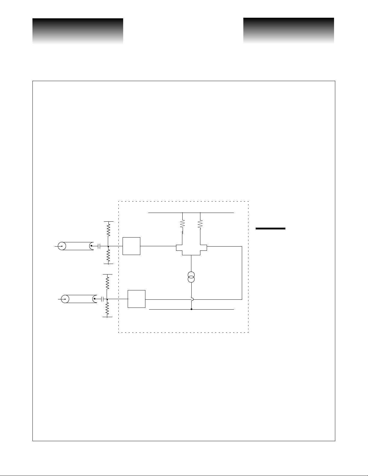
Figure 14: AC Termination of Low-Speed LVPECL REFCLK and LPTIMCLK Inputs
Chip Boundary
VCC = 3.3V
V
CC
R1
Z
O
C
IN
supply instead of to VEE.
CC
R1||R2 = Zo , R1 = 83Ω R2 =125Ω
VCCR2 + VEER1
R1+R2
= V
BIAS
EE
CC
C
EE
R2
R1
IN
R2
= 0V
V
EE
CIN TYP = 100nF
for AC operation
V
V
Z
O
V
Reference Clock Inputs
The incoming low-speed reference clock inputs are rece ived by differential LVPECL inputs REFCLK± .
Off-chip termination of these inputs is required (see Figure 14).
In most situations these inputs will have high transition density and little DC offset. However, in cases
where this does not hold, direct DC connection is possible. All serial clock inputs have the same circuit topology, as shown in Figure 14. If the input signal is driven differentially and DC-coupled to the part, the mid-point
of the input signal swing should be centered about the input comm on-mode voltage V
and not exceed the
CM
maximum allowable amplitude. For single -ended , DC-coupling operat ions, it is re commended tha t the user provides an external reference voltage. The external reference should have a nominal value equivalent to the common-mode switch point of the DC-coupled signal, and can be connected to either side of the differential gate.
Page 10
741 Calle Plano, Camarillo, CA 93012 • 805/388-3700 • FAX: 805/987-5896 9/6/00
VITESSE SEMICONDUCTOR CORPORATION
G52251-0, Rev. 4.0
VITESSE
SEMICONDUCTOR CORPORATION
Data Sheet
SC8140
Z
O
VREFIN
VREFOUT
2.48832Gb/s 16:1 SONET/SDH
Transceiver with Integrated Clock Generator
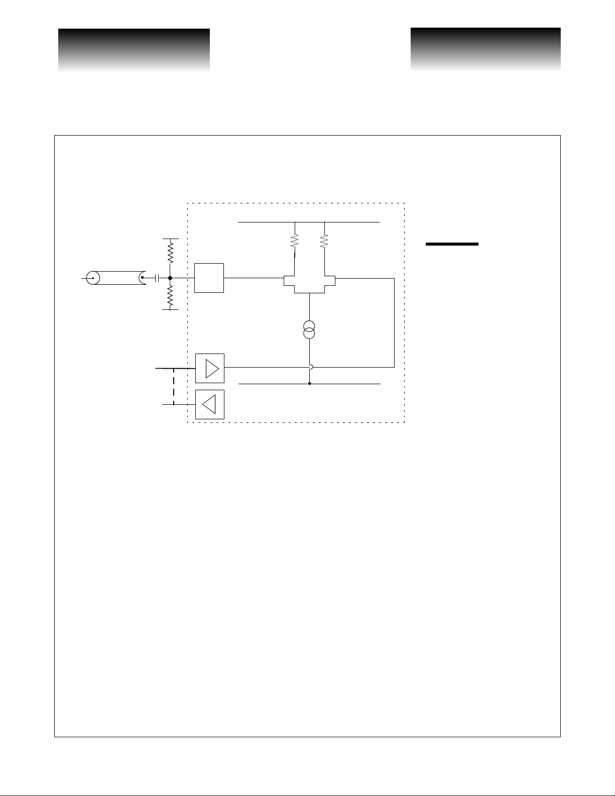
Figure 15: Termination of Low-Speed LVPECL TXIN[15:0] Inputs
Chip Boundary
VCC = 3.3V
V
CC
R1
C
IN
EE
R2
= 0V
V
EE
V
R1||R2 = Zo , R1 = 83Ω R2 =125Ω
VCCR2 + VEER1
R1+R2
= V
CIN TYP = 100nF
for AC operation
BIAS
Low-Speed Inputs
The incoming low-speed inputs are received by single-ended LVPECL inputs TXIN[15:0]. A reference
voltage is necessary to provide for optimal switching of the inputs. The user can either provide an input voltage
reference from the upstream de vice (VREFIN), or ca n use the reference volta ge provided from the VSC8140
(VREFOUT). Side-by-side placement of the VREFIN and VREFOUT pins facilitates easy implementation.
For DC or AC operation, the external reference should have a nominal value equivalent to the commonmode switch point of an LVPECL DC-coupled signal, and adhere to the DC characteristics as specified by the
Table 3 DC characteristics (V
G52251-0, Rev. 4.0
9/6/00 741 Calle Plano, Camarillo, CA 93012 • 805/388-3700 • FAX: 805/987-5896
).
CM
VITESSE SEMICONDUCTOR CORPORATION
Page 11
 Loading...