

VITESSE VSC8132QR Datasheet
Preliminary Data Sheet
VITESSE
SEMICONDUCTOR CORPORATION
VSC8132
2.488Gb/s 1:32 SONET/SDH Demux
Features
• 2.488Gb/s 1:32 Demultiplexer
• SONET STS-48/SDH STM - 16
• HSPECL Differential Serial Data and Clock
Inputs
• 32-Bit TTL Parallel Data Outputs with Odd/
Even Parity Check
• Frame Detect Synchronization
• 77.76, 51.84, and 38.88MHz TTL Clock Outputs
• Single 3.3V supply
• Loss of Clock Alarm
• Loss of Data Alarm
• 2.05W Max Power Dissipation
• 128-Pin PQFP Package
General Description
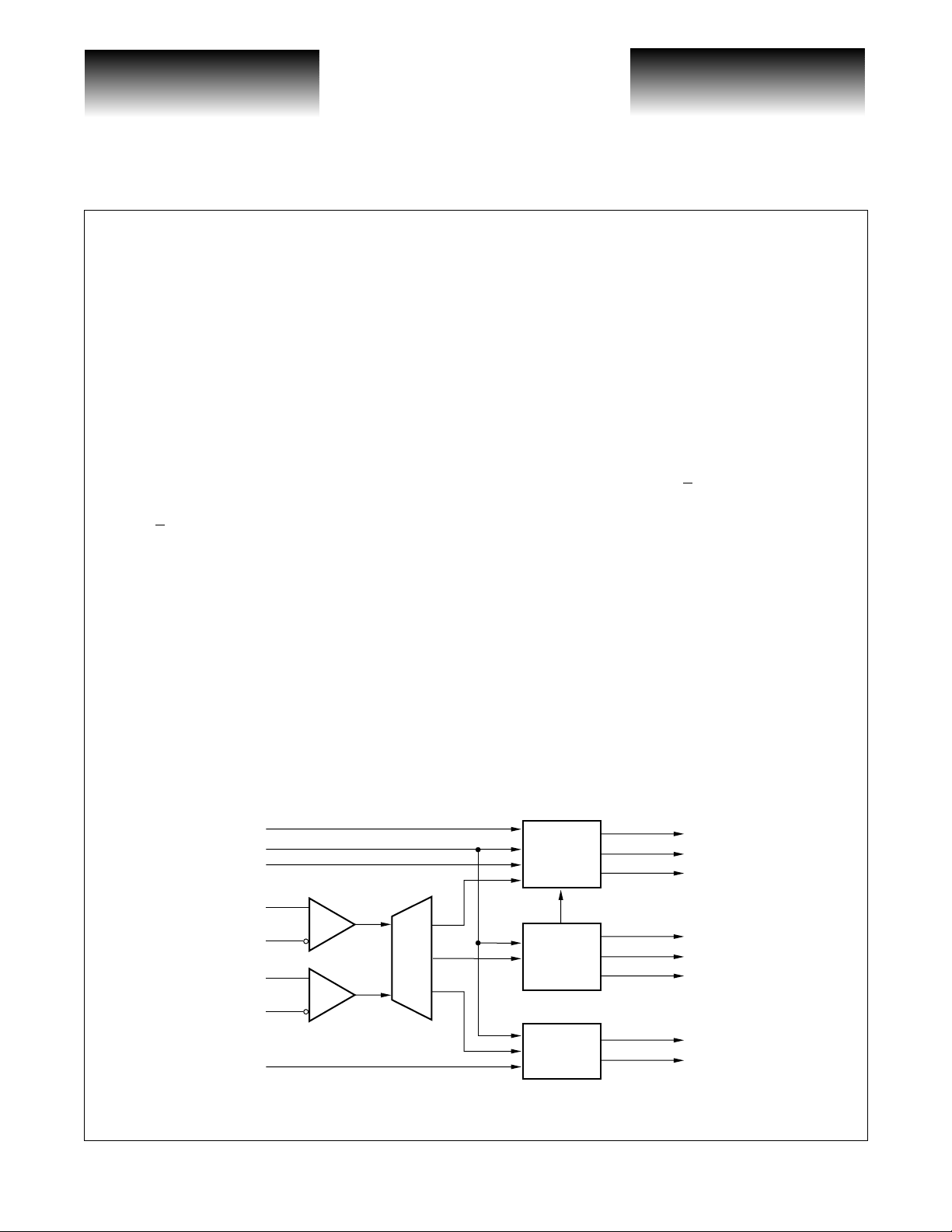
The VSC8132 demultiplexes a 2.488Gb/s HSPECL serial input datastre am (DI+) to 32-bit wide, TTL
77.76Mb/s parallel data outputs D[31:0] for SONET/SDH applications . A 2.488GHz HSPECL input clock
(CLKI+
and 38.88MHz, are generated for upst ream d evi ces ( DATACLK78, CLK51, C LK38 ). Odd or ev en pa r ity i s per formed on the incoming high-speed data via the TTL Parity Select input (PARSEL), and a TTL Parity output
(PARITY) is provided to indicate parity of the input data. Frame Detect on the incoming data is controlled via
the Frame Detect Inhibit (OOFN) and Reset (RESET) TTL inputs. A frame detect monitors the incoming data
steam and screens for 2 bits in A1 byte out of the 8 bits and 2 bits of A2 byte out of the 8 bits. When a Frame
Detect occurs, a synchronization TTL output (SYNC) will be set. Alarm indicators are used to monitor the
activity of the clock and data with TTL compatible control inputs (ALMRESET) and outputs (DTALARM,
CKALARM).
mally-enhanced 128-pin, 14x20x2mm PQFP package.
) is used to time the incoming data and 3 TTL clock outputs, at frequencies of 77.76MHz, 51.84MHz,
Only a single 3.3V power supply is required for device operation. The VSC8132 is packaged in a ther-
VSC8132 Block DIagram
OOFN
RESET
PARSEL
DI+
DI–
CLKI+
CLKI–
ALMRESET
G52250-0, Rev 3.1 Page 1
12/7/00
© VITESSE SEMICONDUCTOR CORPORATION • 741 Calle Plano • Camarillo, CA 93012
Tel: (800) VITESSE • FAX: (805) 987-5896 • Email: prodinfo@vitesse.com
1:32
Demux
Internet: www.vitesse.com
Framing
and
Parity
Clock
Generation
Alarms
DATA[3:0]
SYNC
PARITY
DATACLK78
CLK51
CLK38
DTALARM
CKALARM
VITESSE
SEMICONDUCTOR CORPORATION
Preliminary Data Sheet
2.488Gb/s 1:32 SONET/SDH Demux
VSC8132
Functional Description
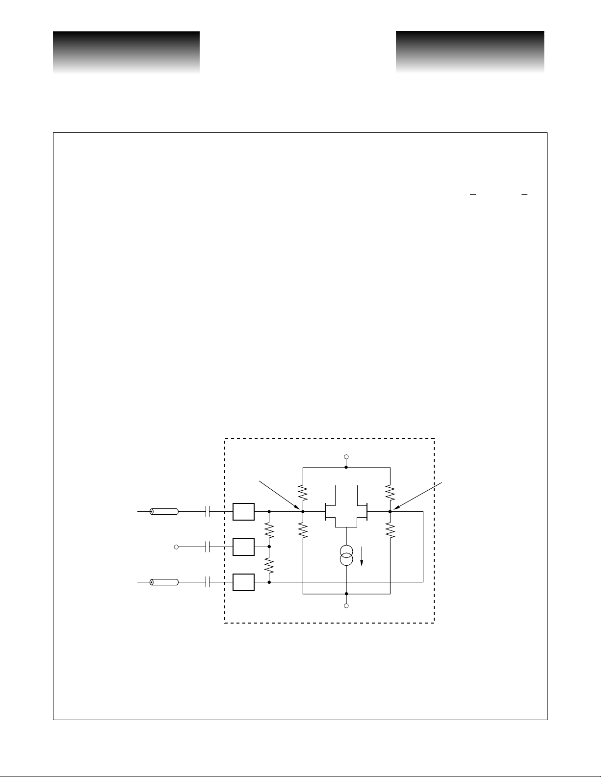
High-Speed Clock and Data Interface
The incoming high-speed data and high-speed clock are received by high-speed inputs DI+ and CLKI+.
The inputs are internally biased to accommodate AC-coupling.
The data and clock inputs are internally terminated by a center-tapped resistor network. For differential
input DC-couplin g, the network is terminated to the appropriate termination voltage,
V
termination for both true and complement inputs. For differential input AC-coupling, the network is ter-
TERM
minated to
V
via a blocking capacitor.
TERM
In most situations, these inputs will have high transition density and little DC offset. However, in cases
where this does not hold, direct DC connection i s possible . All serial data and clock in puts have t he same circuit
topology as shown in Figure 1. The reference voltage is created by a resistor divider as shown. If the input signal is driven differentially and DC-coupled to the part, the mid-point of the input signal swing should be centered about this reference voltage and not exceed the maximum allowable amplitude. For single-ended, DCcoupling operations, it is recommended th at the user provides an externa l reference voltage whic h has better
temperature and power supply noise rejection than the on-chip resistor divider. The external reference should
have a nominal value equivalent to the common mode switch point of the DC-coupled signal, and can be connected to either side of th e differential gate.
Figure 1: High-Speed Clock and Data Inputs
V
providing a 50 Ω to
TERM
V
Z
TERM
Z
Chip Boundary
V
= 3.3V
CC
C
IN
0
0
100nF
C
AC
100nF
C
IN
100nF
1.65V
50Ω
50Ω
3kΩ
3kΩ
3kΩ
3kΩ
I
I
= 0V
V
EE
1.65V
Page 2 G52250-0, Rev 3.1
© VITESSE SEMICONDUCTOR CORPORATION • 741 Calle Plano • Camarillo, CA 93012
Tel: (800) VITESSE • FAX: (805) 987-5896 • Email: prodinfo@vitesse.com
Internet: www.vitesse.com
12/7/00

Preliminary Data Sheet
VITESSE
SEMICONDUCTOR CORPORATION
VSC8132
Low-Speed Data Interface
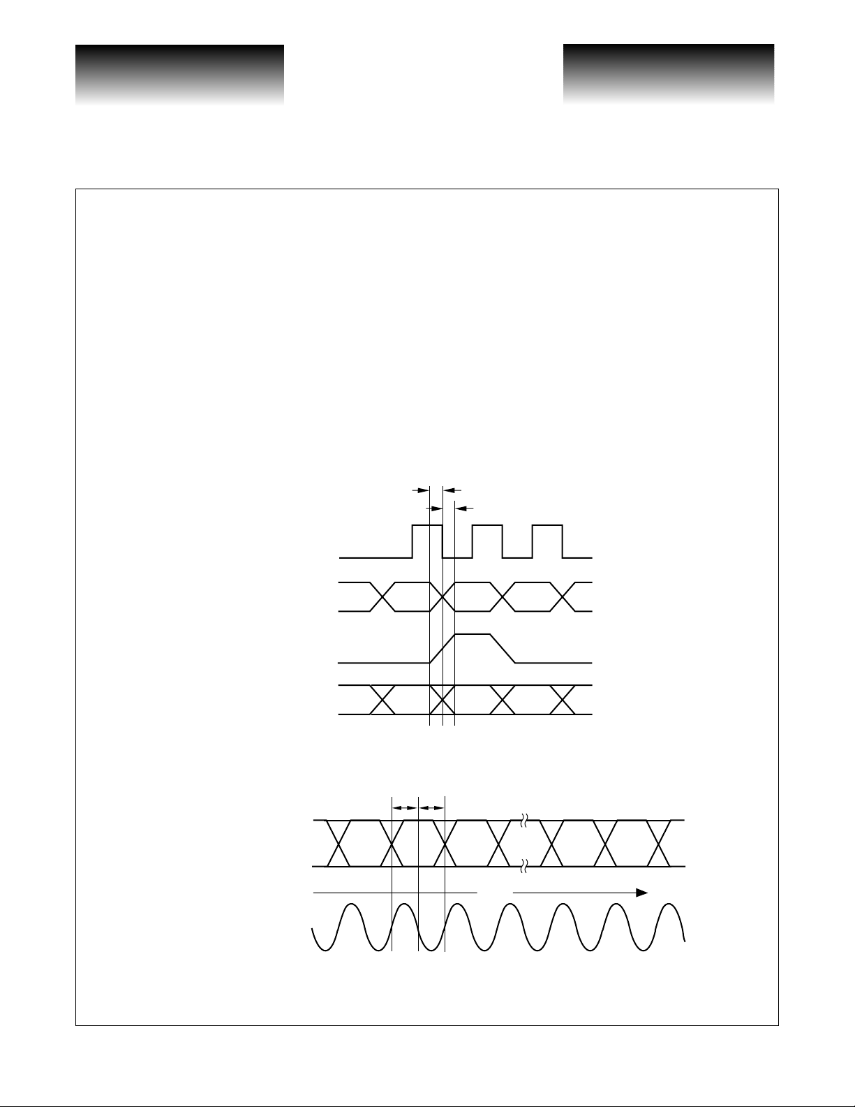
The 77.76Mb/s parallel data outputs D[31:0] are clocked out of the VSC8132 on the falling clock edge of
the 77.76MHz output clock (DATA78CLK). The data and clock are TTL levels. The MSB (D31) bit is the first
bit into the serial interface.
Parity Selection
The parity output bit (PARITY) is clocked out on the falling edge of the 77.76MHz clock (DATA78CLK).
This bit indicates the parity of the 32 bits of data along with the frame sync bit. The parity of the output is determined by the parity select in put ( PARSEL). When t he parit y select in put is L OW, the outp ut pari ty is od d. When
the parity select is HIGH, the output parity is even. The parity inputs and outputs are TTL levels. See Figure 2
for output timing relationship.
Framing Logic Interface
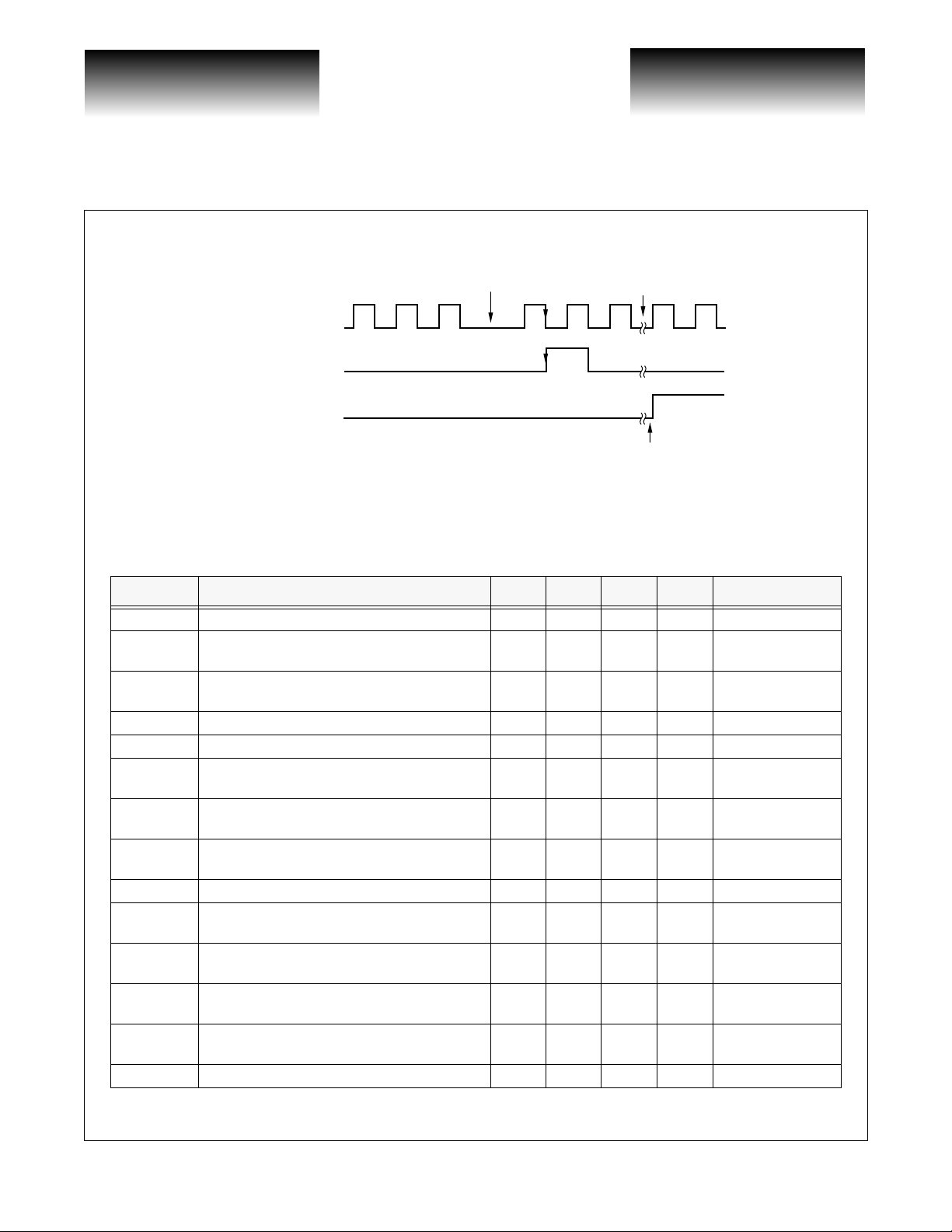
When a frame detect occurs and t he f ra me d ete ct i nh ib it input ( OOFN) i s set L OW, the frame det ect output
(SYNC) is set HIGH on the negative edge of the 77.76MHz clock and on the 3rd set of four A2 bytes at the 32bit data output. The frame detect mechanism is inhibited when the frame detect inhibit (OOFN) input is set
HIGH. The frame detect output and frame detect inhibit are TTL levels.
NOTE: The 77.76MHz clock miss es one clock cycle during a frame detect. This m issed cycle oc curs one
clock period before the Sync pulse is set HIGH (see Figure 4).
To use as a framer:
Step 1: Set OOFN LOW
Step 2:Wait for Sync pulse
Step 3:When Sync Pulse goes HIGH, set OOFN HIGH
2.488Gb/s 1:32 SONET/SDH Demux
Chip Reset
Chip reset (RESET) will reset the framing logic so that no fram e detection barrel shift ing is performed.
Therefore, if the fra me d ete ct inh ibit inp ut is set h igh , the ch ip w ill ac t as a sim ple de mux afte r re set. T he reset
should be set high for 16 clock cycles of the high speed clock input. The chip reset is a TTL level.
Alarm Logic Interface
The Loss of Clock (CKALARM) and Loss of Data (DTALARM) alarms monitor the activity of the clock
and data. The Alarm Reset (ALMRESET) input controls the alarm activity . Polling of the alarms signals are initiated by toggling the Alar m Reset in put HIGH and the n LOW on e ti me. To reset both alarm output s, th e Alar m
Reset should be toggled HIGH to LOW two times. All alarm logic interface signals are TTL levels.
Supplies
The VSC8132 is specified as a HSPECL/TTL device with a single positive 3.3V supply. Normal operation
is to have V
a negative 3.3V supply, V
put signals are still referenced to V
G52250-0, Rev 3.1 Page 3
12/7/00
= +3.3V and V
CC
© VITESSE SEMICONDUCTOR CORPORATION • 741 Calle Plano • Camarillo, CA 93012
= ground. Should the user desire to use the device in a ECL environment with
EE
will be ground and VEE will be -3.3V. If used with VEE tied to -3.3V, the TTL out-
CC
.
EE
Tel: (800) VITESSE • FAX: (805) 987-5896 • Email: prodinfo@vitesse.com
Internet: www.vitesse.com
VITESSE
SEMICONDUCTOR CORPORATION
Preliminary Data Sheet
2.488Gb/s 1:32 SONET/SDH Demux
Decoupling of the power supplies is a critical element in maintaining the proper operation of the part. It is
recommended that the V
on each V
power supply pin as close to the package as possible. If room permits, a 0.001µF capacitor should
CC
also be placed in parallel with the 0.1
low-inductance ceramic SMT X7R devices. For the 0.1
0.01
µF and 0.001µF capacitors can be either 0603 or 0402 packages.
For low frequency decoupling, 47
power supply be decoupled using a 0.1µF and 0.01µF capacitor placed in parallel
CC
µF and 0.01µF capacitors mentioned above. Recommended capacitors are
µF capacitor, a 0603 package should be used. The
µF tantalum, low-inductance SMT caps should be sprink led over the
board’s main +3.3V power supply and placed close to the C-L-C pi filter.
If the device is being used in an ECL environment w ith a -3.3V supply, all references to decoupling V
must be changed to VEE, and all references to decoupling 3.3V must be changed to -3.3V.
AC Characteristics
Figure 2: Output Timing
t
PD1
t
PD2
78MHz CLK
VSC8132
CC
78MHz DATA
SYNC PULSE
PARITY
DI+
Differential Serial Data Input
CLKI+
Differential Clock Input
Figure 3: Data Output Timing
t
SERSU
D31 D0
MSB
NOTE: Bit 31 (MSB) is received first, Bit 0 (LSB) is received last.
t
SERHO
Time
LSB
Page 4 G52250-0, Rev 3.1
© VITESSE SEMICONDUCTOR CORPORATION • 741 Calle Plano • Camarillo, CA 93012
Tel: (800) VITESSE • FAX: (805) 987-5896 • Email: prodinfo@vitesse.com
Internet: www.vitesse.com
12/7/00
Preliminary Data Sheet
VITESSE
SEMICONDUCTOR CORPORATION
VSC8132
2.488Gb/s 1:32 SONET/SDH Demux
Figure 4: Framing Sequence
Missed Clock
(1)
Pulse
OOFN (In)
(1)
(asynchronous)
CLK78 (Out)
SYNC PULSE (Out)
NOTE: (1) No missing clock pulse for CLK78 when VSC8132 is working as a dumb demux.
Once frame occurs and OOFN is set HIGH, the no framing will occur until
OOFN is set LOW again. The VSC8132 will remain framed with SONET frame.
Approximately <110µs
Set HIGH, less than 110µs
after SYNC goes HIGH
T a ble 1: AC Characteristics
Parameters Description Min Typ Max Units Conditions
t
DATApd
t
CLKRpd
t
CLKFpd
t
DEDGE
t
CLKEDGE
t
CONEDGE
t
SERSU
t
SERHO
f
MAX
t
CLK38Rpd
t
CLK38Fpd
t
CLK51Rpd
t
CLK51Fpd
, t
t
PD1
PD2
Data Valid From Falling Edge of 77.76MHz 230 1250 ps External load = 5pf
High-speed Clock Rising Edge to 77.76M Hz
Clock Rising Edge
High-Speed Cl oc k R i si ng E dg e to 77 .7 6MHz
Clock Fallin g Edge
2.5 8.0 ns External load = 5pf
2.3 7.1 ns External load = 5pf
D[0:31] Edge Rate (10%-90%) - 2.0 ns External load = 5pf
77.76, 51.84, 38.88MHz Edge Rates (10%-90%) - 2.0 ns External load = 5pf
Control Signals (SYNC, PARITY, DTALARM,
and CKALARM) Edge Rate (10%-90%)
DI+ Setup Time with Respect to Falling Edg e of
CLKI+
DI+ Hold Time with Respect to Falling Edge of
CLKI+
-2.0ns
100 - ps See Figure 3
75 - ps See Figure 3
External load = 5pf
Demux Input Maximum Clock Frequency - 2.9 GHz
High-Speed Cl oc k R i si ng E dg e to 38 .8 8MHz
Clock Rising Edge.
High-Speed Cl oc k R i si ng E dg e to 38 .8 8MHz
Clock Fallin g Edge
High-Speed Cl oc k R i si ng E dg e to 51 .8 4MHz
Clock Rising Edge
High-Speed Cl oc k R i si ng E dg e to 51 .8 4MHz
Clock Fallin g Edge
2.0 6.3 ns External load = 5pf
2.0 5.9 ns External load = 5pf
2.0 6.0 ns External load = 5pf
2.0 5.9 ns External load = 5pf
Data Invalid Window 0, 230 0, 1250 ps
G52250-0, Rev 3.1 Page 5
12/7/00
© VITESSE SEMICONDUCTOR CORPORATION • 741 Calle Plano • Camarillo, CA 93012
Tel: (800) VITESSE • FAX: (805) 987-5896 • Email: prodinfo@vitesse.com
Internet: www.vitesse.com
 Loading...