

VITESSE VSC8124RE Datasheet

VITESSE SEMICONDUCTOR CORPORATION Page 1
2/23/00 741 Calle Plano, Camarillo, CA 93012 • 805/388-3700 • FAX: 805/987-5896
VITESSE
SEMICONDUCTOR CORPORATION
Target Specification
VSC8124
2.488 Gb/s Quad
Data Re-timer
G52271-0, Rev. 1.14
Features
General Description
The VSC8124 is a four channel, 2.5 Gb/s data re-timer for cleaning up data downstream of optical links or
cross point switches. Serial data at the 2.5 Gb/s rate is independently re-timed on four channels, and driven differentially by CML drivers. The re-timing function on each channel can be individually bypassed for lower rate
signals or test purposes. The VSC8124 provides four independent loss of signal indicators in the event of loss of
synchronous data transitions.
• Four Channel 2.488 Gb/s Data Recovery
• SONET Quality Jitter Tolerance
• Fastlock Data Acquisition less than 200
Bit Times
• Loss of Signal Indicators
• Long Strings of Static Data Tolerated by the
Clock Recovery Circuit without Loss of Signal
• First Order Clock Recovery Loop Minimizes
Jitter Accumulation
• Differential on Chip Terminated Serial Data I/O
• Bypass for OC3, OC12 Data Rates
• 155.52 MHz Reference Clock Frequency
• 3.3V Supply Operation
• 14 x 14mm, 100 Pin Thermally Enhanced
TQFP Package
VITESSE
SEMICONDUCTOR CORPORATION
2.488 Gb/s Quad
Data Re-timer
Target Specification
VSC8124
Page 2 VITESSE SEMICONDUCTOR CORPORATION
741 Calle Plano, Camarillo, CA 93012 • 805/388-3700 • FAX: 805/987-5896 2/23/00
G52271-0, Rev. 1.14
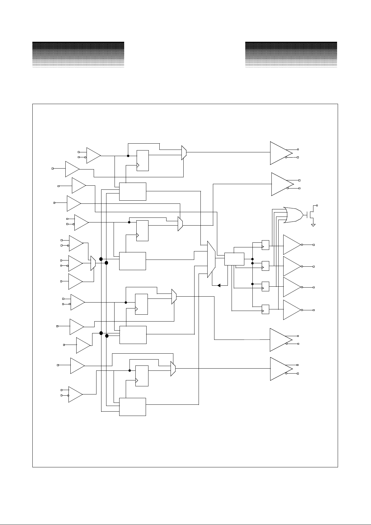
VSC8124 Block Diagram
Clock
Recovery
Unit
Clock
Recovery
Unit
Clock
Recovery
Unit
Clock
Recovery
Unit
SD3+
SD3-
RDAT3+
RDAT3-
RDAT2+
RDAT2-
RDAT1+
RDAT1-
RDAT0+
RDAT0-
LOS
Logic
LOS3N
LOS2N
LOS1N
LOS0N
LOSALMN
SD0+
SD0-
SD1+
SD1-
SD2+
SD2-
REFCK0+
REFCK0-
PECL
CML
CML
CML
CML
TTL
TTL
TTL
TTL
CML
CML
LOSREL
REFCK1+
REFCK1-
PECL
REFCK+
TTL
0
1
TTL
1
0
TTL
RTBYP3
TTL
RTBYP2
1
0
TTL
FASTLOCK
TTL
RTBYP1
1
0
TTL
RTBYP0
1
0
CML
CML
VITESSE SEMICONDUCTOR CORPORATION Page 3
2/23/00 741 Calle Plano, Camarillo, CA 93012 • 805/388-3700 • FAX: 805/987-5896
VITESSE
SEMICONDUCTOR CORPORATION
Target Specification
VSC8124
2.488 Gb/s Quad
Data Re-timer
G52271-0, Rev. 1.14
Functional Description
Reference Clock
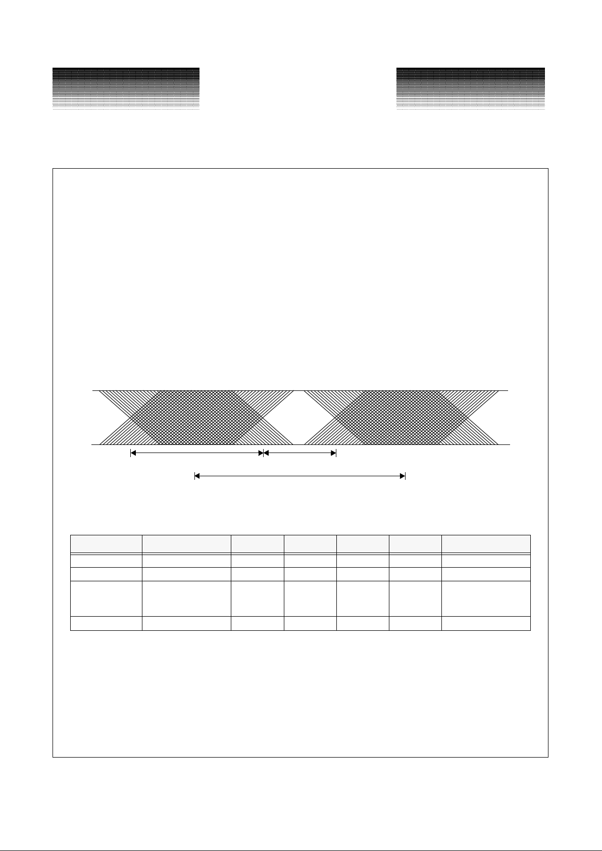
A clean reference clock should be provided to meet jitter specifications. An arbitrary discontinuity in refer-
ence clock phase can be tolerated without data error at slightly reduced jitter tolerance. (See Table 1) Phase
changes must not occur more often than every 20 µs. Serial data transition density must average for that
period. Two reference clock input ports are provided. The REFSEL pin selects the active port. When REFSEL
is not driven, it floats low, selecting REFCK0. Changing REFSEL implies a phase change.
Clock Recovery
The incoming serial data on each channel is presented to a clock recovery and data re-timing circuit. For
each channel, a phase detector and low pass filter force a local clock to track the average phase of the incoming
serial data. The low pass filter is first order to prevent jitter peaking in cascaded devices.
Figure 1: Serial Input Data Eye Diagram
Table 1: Serial Input Data Specification
NOTE: 1) Jitter tolerance is measured at worst case power supply and temperature, using 155.52 MHz clean reference clock
(REFCK to meet 2.0 ps RMS jitter at less than 10 Mhz in bandwidth), and 600mV swing differential PRBS data
with150ps maximum rise time.
2) Jitter tolerance and re-timed data jitter are degraded in FASTLOCK mode.
3) Reference clock frequency tolerance: ∆f <= 100 ppm
4) Jitter tolerance specifications do not apply in re-timer bypass mode.
Parameter Description Min Typ Max Units Conditions
J
T
Jitter tolerance 220 - - ps Normal Operation
J
T
Jitter tolerance 150 170 - ps Fast Lock Mode
J
T
Jitter tolerance 190 210 - ps
Within 20µs after
REFCLK phase
change
Period - 401.88 - ps
0.5
≥
J
T
Eye Opening
Period
VITESSE
SEMICONDUCTOR CORPORATION
2.488 Gb/s Quad
Data Re-timer
Target Specification
VSC8124
Page 4 VITESSE SEMICONDUCTOR CORPORATION
741 Calle Plano, Camarillo, CA 93012 • 805/388-3700 • FAX: 805/987-5896 2/23/00
G52271-0, Rev. 1.14
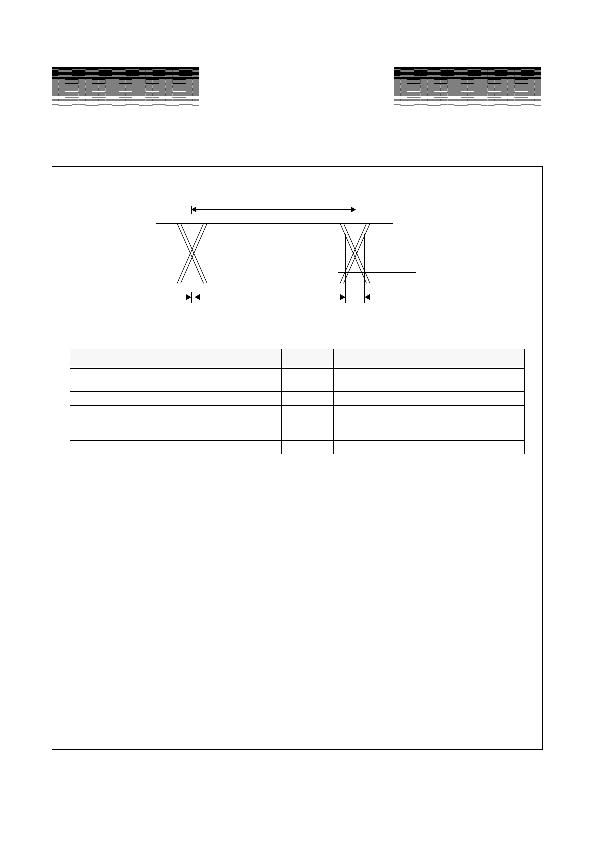
Figure 2: Re-timed Serial Output Data Eye Diagram
Table 2: Serial Output Data Specification
NOTES: 1) Jitter generation is measured at worst case power supply and temperature using 155.52 MHz clean reference clock
and clean serial data.
2) Jitter generation and rise, fall time specifications do not apply in re-timer bypass mode.
Parameter Description Min Typ Max Units Conditions
J
G
Jitter generation - -
12ps rms
Normal Operation
J
G
Jitter generation - - 15 ps rms Fast Lock Mode
J
G
Jitter generation - - 14ps rms
Within 40 µs after
REFCK phase
change
tr, t
f
Rise time, fall time - - 140 ps 20 to 80%
Period
J
G
80%
20%
tr t
f
,
VITESSE SEMICONDUCTOR CORPORATION Page 5
2/23/00 741 Calle Plano, Camarillo, CA 93012 • 805/388-3700 • FAX: 805/987-5896
VITESSE
SEMICONDUCTOR CORPORATION
Target Specification
VSC8124
2.488 Gb/s Quad
Data Re-timer
G52271-0, Rev. 1.14
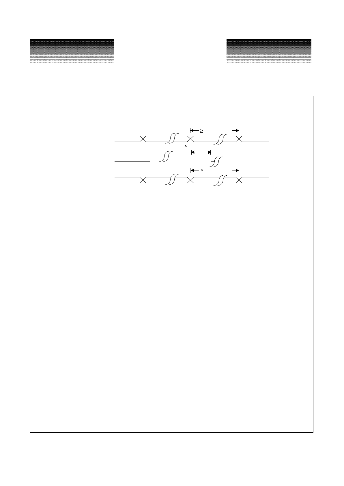
Figure 3: Fastlock Timing Diagram
Fast Lock
The VSC8124 supports a fastlock clock recovery mode which enables the clock recovery unit to lock the
retiming clock to the incoming data within 80 bit periods of initiation. As a requirement for the operation of the
fastlock function, the driving system must send a 0101 bit pattern while the fastlock pin is at a high logic level.
The FASTLOCK function is active simultaneously on all four data channels The fastlock pin has a TTL input
receiver meeting the specifications contained in Table 7. Note that jitter tolerance and re-timed data jitter are
degraded in FASTLOCK mode.
Loss of Signal
The loss of signal (LOS) circuitry is shared among four serial data channels, sampling the signal condition
on each channel sequentially. There is a loss of signal latch and active low indicator pin (LOS[0:3]N) for each
channel. In addition, there is an alarm pin (LOSALMN) which indicates the OR of the latched states of the four
channel indicators. The alarm pin uses an open drain output, so the alarm pins from multiple parts can be wired
together. A weak external pull resistor (approximately 1k Ohm) must be provided to utilize the wired NOR
alarm function. To facilitate system troubleshooting, the LOS latches can only be cleared by the active high
LOSCLR input.
The loss of signal clear (LOSCLR) input will cause all four loss of signal indicators LOS[0:3]N and the loss
of signal alarm (LOSALM) to be cleared. The LOSCLR input is asynchronous. It must be held active for at
least two reference clock cycles. A channel found to be missing after the error latch has been cleared, will again
set its error latch and the LOSALMN.
The LOS circuit examines a selected clock recovery channel for expected data transition activity. Expected
data activity includes pseudo-random data at a baud rate 16 times the reference clock frequency, and data
including at least 8500 consecutive bits of a 101010... pattern. The detector will allow the OC-48 framing pattern to pass without triggering LOS. The LOS detector is disabled when FASTLOCK mode is active.
To assist diagnostic procedures, the effect of individual loss of signal indicators in the loss of signal alarm
can be masked. This is controlled by the MASK[0:3] pins. Each of those pins, when pulled high, disables the
effect of its respective channel on the loss of signal alarm (LOSALM). If all MASK pins are pulled high, the
LOSALM signal will not pull down. The loss of signal indicators for individual channels are not affected by the
MASK pins.
1010...
Valid Data
Valid DataInput Data
Output Data
Fastlock
200 Bit Times
200 Bit Times
80 Bit Times
Valid Data
Valid Data
VITESSE
SEMICONDUCTOR CORPORATION
2.488 Gb/s Quad
Data Re-timer
Target Specification
VSC8124
Page 6 VITESSE SEMICONDUCTOR CORPORATION
741 Calle Plano, Camarillo, CA 93012 • 805/388-3700 • FAX: 805/987-5896 2/23/00
G52271-0, Rev. 1.14
Re-timer Bypass
The serial data re-timer can be individually bypassed for data channels. This allows asynchronous data signals to pass through the part. The bypass function is controlled by the RTBYP[0:3] pins.
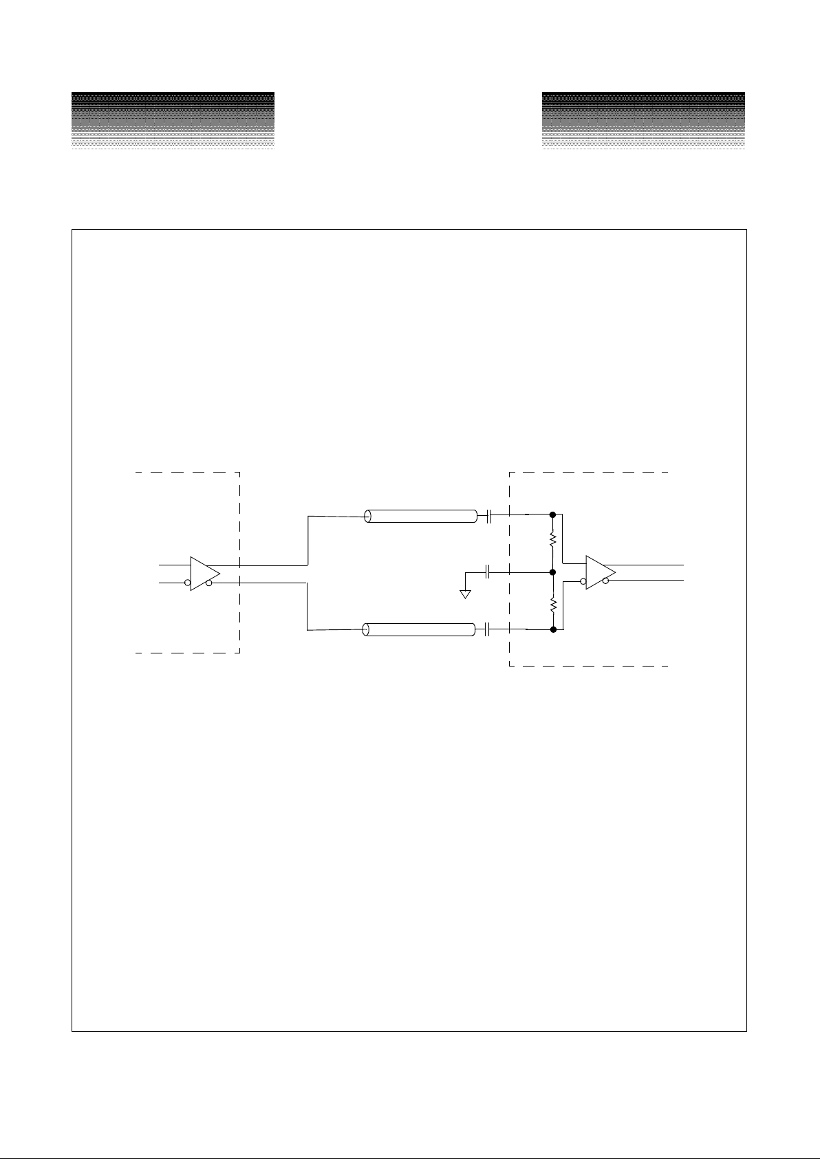
High Speed Interfaces
Figure 4: High Speed Data Input Termination- AC Coupled
Notes:
1)It is recommended that VTERM pins from multiple inputs NOT be tied together, unless driven from a low impedance supply.
2) The high speed data receivers have self biased inputs.
3) For unused serial data receivers, it is recommended to tie one side low by connecting a 1k Ohm resistor to Vee and letting the other side float.
Quad data Re-timerXpnt switch
0.1 µF
0.1 µF
Zo = 50Ω
Zo = 50Ω
DI
50Ω
DIN
50Ω
VTERM
 Loading...