

VITESSE VSC8123 Datasheet
VITESSE
SEMICONDUCTOR CORPORATION
Product Summary
VSC8123
10Mb/s to 2.7Gb/s Rate Agile,
Adaptive Clock and Data Recovery
Features
• Continuous NRZ Frequency Coverage from
10Mb/s to 2.7Gb/s data rates
• Programmable Acquisition and Tuning of Frequency,
Phase and Voltage—No Reference Clock Required
• Built-In Bit L evel Error Rat e Monitoring Opera te s
Independently of In-Service Data Channel
• User-Definable Control Algorithms fo r
Acquisition, Tracking, and Error Profiling
• Integrated High-Gain AGC Front End with
Offset Correction and On-Die Termination
• Secondary High-Level Input for Backup Data
Input or hint/LOS Clock
• 80-Pin PQFP Package
General Description
The VSC8123 is a universal clock and data recovery system designed for a broad range of system applications. The integrated frequency synthesizer provides continuous coverage from 10Mb/s to OC-48+FEC data
rates with SONET quality output. In addition to its broadband capability, the VSC8123 is designed for the most
demanding applications, where signal integrity is low and the absolute maximum voltage and timing margin is
required. The VSC8123 offers signal acquisition capabilities far beyond what conventional CDRs offer, in a
highly monolithic form.
In addition to the bro adband synt hesize r capab ility, the VSC8123 also has the ability to dynamical ly modif y
its acquisition point in both voltage and phase. This enables the VSC8123 to acquire data in the presence of significant symmetry distortion or “bad spots” in the data eye. Integrated voltag e and phase adjust ment is pr o v id ed
to offset the sampling point over the entire voltage and phase range of the input data eye. Additional circuitry is
provided to measure relative bit-error rates without affecting the integrity of the active data stream. Using an
external controll er, the VSC8123 can acq uire fre quency, scan the incoming data eye and au tomati cally se t its
position to optimize margin in both vol ta ge and phase. T hi s opt i mization can be one-time on power-up, or set t o
continuously repeat without taking the d ata stream off-line—no errors will be introduced into the output data
stream as the chip tracks the center of the data eye.
Through the controller interface, the VSC8123 can provide telemetry on the condition of the incoming data
eye and the quality of the acquisition without taking the data off-line, enabling eye profiling, Q-testing, signal
strength measurements, and bit-level error detection/prediction—all non-invasively.
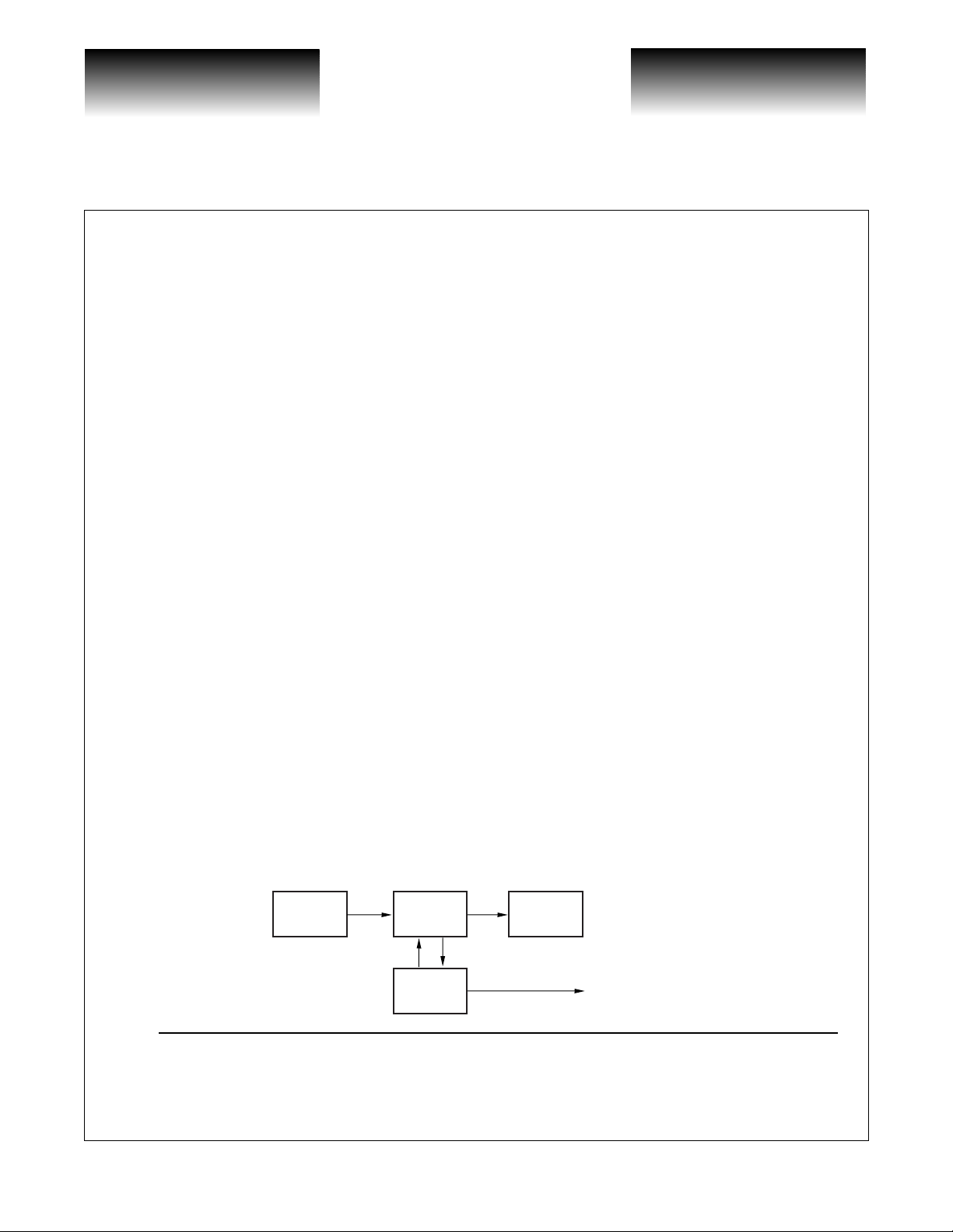
System Block Diagram
TIA
VSC7969
Notice
Vitesse Semiconductor Corporation (“Vitesse”) provides this document for informational purposes only. This document contains pre-production information
about Vitesse products in their concept, development and/or testing phase. All information in this document, including descriptions of features, function s,
performance, technical specification s and availability, is subject to change without notice at any time. Nothing co nta ine d in this document shall be construed
as extending any warrant y or pr omis e, express or im plie d, tha t any Vitesse produ ct wi ll be available as descr ibe d or wi ll be su itable for or will accomplish
any particular task.
Vitesse Semiconductor Corporation’s products are not intended for use in life support appliances, devices or systems. Use of a Vitesse product in such applications without written consent is pr ohi bited.
PS120500 Page 1
© VITESSE SEMICONDUCTOR CORPORATION • 741 Calle Plano • Camarillo, CA 93012
Tel: (800) VITESSE • FAX: (805) 987-5896 • Email: prodinfo@vitesse.com
CDR
VSC8123
Controller
Internet: www.vitesse.com
Transceiver or
Demultiplexer
VSC8145
VSC8141
System Interface
 Loading...