

VITESSE VSC8122QP Datasheet

VITESSE
SEMICONDUCTOR CORPORATION
Data Sheet
VSC8122
Multi-Rate SONET/SDH
Clock and Data Recovery IC
Features
• Multi-Rate OC-3, OC-12, OC-24, OC-48 Clock
and Data Recovery
• Supports Gigabit Ethernet
• Differential Back Terminated I/O
• Maintains Clock Output in the Absence of Data
• Selectable Reference Clock
• Loss of Lock Indicator
• Exceeds SONET/SDH Requirements for Jitter
Tolerance, Jitter Transfer and Jitter Generati on.
• 3.3V Supply Ope r ation
• 1W Typical Power
• 64-pin , 10x10mm PQFP Packaging
General Description
The VSC8122 is a single-chip clock recovery IC for use in SONET OC-48, OC-24, OC-12, OC-3, or Giga-
bit Ethernet systems operating at their respective 2.48832Gb/s, 1.24416Gb/s, 622.08Mbps, 155.52Mbps, or
1.25Gbps data rates. The VSC8122 complies with SONET jitter tolerance, jitter transfer and jitter generation
specifications.
Alarm functions support typical telecom system applications. The Loss of Lock (LOL) output indicates
when the devic e goes out of lock, which wo uld most of ten occu r in the e v ent of a loss of v ali d dat a. The NOREF
output flags when the reference input to the VSC8122 either is removed, or goes severely out of tolerance.
VSC8122 Block Diagram
DI+
DI-
REFCK1 +/REFCK0 +/-
Ph/Freq.
Detector
REF_INPUTSEL
FILTO+/-
Divider
FILTI+/-
Loop
Filter
REF_SEL[1:0]
VCO
FSEL[1:0]
Divider
Data
Retiming
Lock
Detect
CO+
CO-
DO+
DO-
LOL
NOREF
G52228-0, Rev 4.1 Page 1
01/05/01
© VITESSE SEMICONDUCTOR CORPORATION • 741 Calle Plano • Camarillo, CA 93012
Tel: (800) VITESSE • FAX: (805) 987-5896 • Email: prodinfo@vitesse.com
Internet: www.vitesse.com
VITESSE
SEMICONDUCTOR CORPORATION
Multi-Rate SONET/SDH
Clock and Data Recovery IC
Data Sheet
VSC8122
Functional Description
Data Input
The data input receiver is internally terminated by a center-tapped resistor network. For differential input
AC coupling, the network is terminated to the appropriate termination voltage, V
capacitor, C
to ground. The input requires a differential signal with a peak-to-peak voltage on both the true
AC
and complement of a minimum of 250mV. These inputs are required to be AC-coupled to allow use with a variety of limiting amplifiers.
Figure 1: Input Termination (AC-Coupled)
VSC8122Limiting Amp
Zo = 50Ω
0.1 µF
C
AC
DI+
50Ω
V
50Ω
TERM
through a blocking
TERM
Z
= 50Ω
o
0.1 µF
DI-
High-Speed Clock and Data Outputs
The VSC8122 high-speed clock and data outputs can be DC-terminated, 50 Ω to VCC as indicated in
Figure 2.
Figure 2: High-Speed Clock and Data Output DC Termination
VSC8122
V
CC
50Ω
50Ω
V
CC
CO+ / DO+
CO- / DO-
100Ω
100Ω
V
CC
Zo = 50Ω
= 50Ω
Z
o
V
CC
Page 2 G52228-0, Rev 4.1
© VITESSE SEMICONDUCTOR CORPORATION • 741 Ca l le Pl an o • Camarillo, CA 93012
Tel: (800) VITESSE • FAX: (805) 987-5896 • Email: prodinfo@vitesse.com
Internet: www.vitesse.com
01/05/01

VITESSE
SEMICONDUCTOR CORPORATION
Data Sheet
VSC8122
Outputs can also be A C t erminated as sho wn in Figure 3 . The ou tput differential voltag e and common-mode
voltage range are specified in Table 4, High-Speed Inputs and Outputs.
Figure 3: High-Speed Clock and Data Output AC Termination
VSC8122
V
CC
100Ω
CO+ / DO+
CO- / DO-
Clock Recovery
100Ω
V
CC
The VSC8122 has a selectable input data rate. Two pins (FSEL0 and FSEL1) select the data rate to be provided to the VSC8122.
0.1µF
0.1µF
Zo = 50Ω
= 50Ω
Z
o
Multi-Rate SONET/SDH
Clock and Data Recovery IC
V
TERM
50Ω
50Ω
V
TERM
Table 1: Input Data Rate Select
Input Data Rate FSEL0 FSEL1
2.48832Gb/s or 2.5Gb/s
1.24416Gb/s or 1.25Gb/s
622.08Mb/s or 625Mb/s
155.52Mb/s or 156.25Mb/s
00
10
01
11
The incoming data is presented both to the clock recovery circuit and the data retiming circuit. When there
is a phase error between the incoming data and the on-chip Voltage-Controlled Oscillator (VCO), the loop filter
raises or lowers the control voltage of the VCO to null the phase difference.
The lock detector monitors the frequency difference between the REFCK (optionally divided by a prescaler) and the reco ve red cl ock di v ided b y 128 . In the event of the loss of an in put signal , or i f the in put i s switching randomly, the VCO will move in one direction. At the time the VCO differs by more than 1MHz from the
REFCK based 2.48832GHz rate, the lock detector will assert the LOL output. LOL is designed to be asserted
from between 2.3µs and 100µs after the interruption of data. The VCO will continue to be frequency-locked at
approximately 1MHz off of the REFCK based 2.48832GHz rate.
When NRZ data is again presented at the data input, the phase detector will permit the VCO to lock to the
incoming data. Hystere sis is p ro vided whi ch del ays the deasserti on of LOL unti l appro ximate ly 160µs f ollo wi ng
the restoration of valid data.
The NOREF output will go high to indicate that there is no signal on the REFCK input, o r that the REFCK
is more than approximately 25% above or below the expected value.
G52228-0, Rev 4.1 Page 3
01/05/01
© VITESSE SEMICONDUCTOR CORPORATION • 741 Calle Plano • Camarillo, CA 93012
Tel: (800) VITESSE • FAX: (805) 987-5896 • Email: prodinfo@vitesse.com
Internet: www.vitesse.com

VITESSE
SEMICONDUCTOR CORPORATION
Multi-Rate SONET/SDH
Clock and Data Recovery IC
Data Sheet
VSC8122
Two sets of reference frequencies for the VSC8122 are shown in Table 2. SONET reference clock frequencies are as indicated, with Gigabit Ethernet frequencies listed in parenthesis. The two different sets of reference
clocks are needed since the reference clock for SONET and Gigabit Ethernet applications will be slightly dif ferent. Internally, the VSC8122 requires a 19.44MHz reference (or 19.53MHz reference for Gigabit Ethernet). The
customer can select to provide either the 19.44MHz reference (or 19.53MHz reference for Gigabit Ethernet), or
the 2x, 4x or 8x of that re fer e nce at 38 .88MHz ( 3 9.06M Hz) , 77.7 6MHz ( 78 .13MHz) o r 155M Hz (156.25MHz).
The REF_SEL[1:0] inputs will program the internal divider as required to use the selected REFCK frequency.
Two reference clock inputs are provided, REFCK1 and REFCK0, to allow “on-the-fly sw itchin g” between
SONET and Gigabit Ethernet applications if desired. Sin ce SONET and Gigabit Ethernet require d if ferent reference clock frequencies, the VSC8122 allows the user to toggle between the two reference clock frequencies
(REFCK1 and REFC K0 ) to su pply the ap pr opria t e in put c loc k. RE F_INP UTS E L is us ed to to ggl e be tw een th e
two reference clock input frequencies; REF_INPUTSEL= “0” selects REFCK0 and REF_INPUTSEL= “1”
selects REFCK1. Either reference cl ock i nput (R EFCK1, REF CK0) can be used for SONET o r Giga bit Et hernet
reference frequencies. LVPECL levels are recommended for REFCK inputs (see Figure 4). If a reference clock
is unused, it is recommended that one of its inputs be tied to V
GND through a 5.1k
Ω resistor.
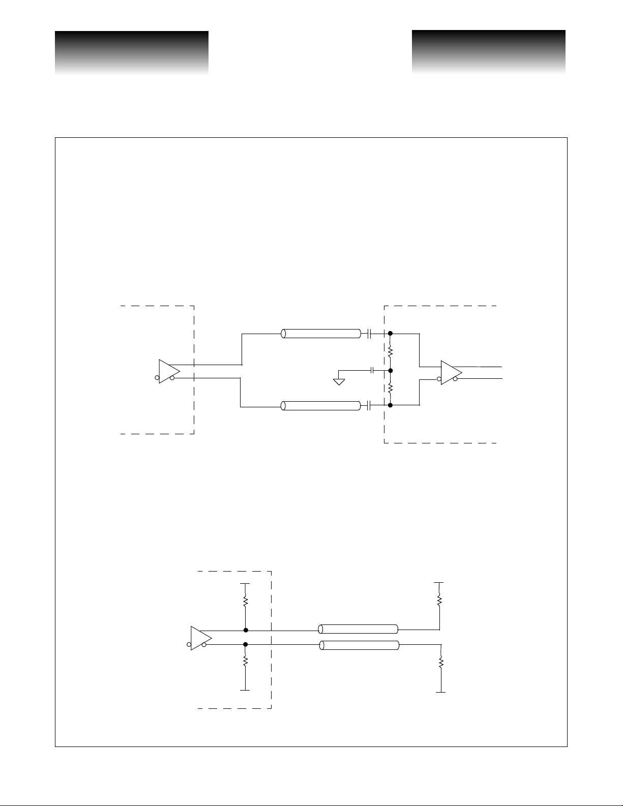
Figure 4: REFCK Input Levels
through a 5.1kΩ resistor, the other one to
CC
LVPECL Level REFCK Inputs (recommended)
NON- LVPECL Level REFCK Inputs
0.1µf
REFCK0 /
REFCK1
50Ω
(1)
VCC-2
NOTES: (1) For differential REFC K input sig nals, 100 Ω termination between true and compleme nt REFCK signals c an be
substituted for the 50
(2) With the input ac-coupled, V
VSC8122
Ω to V
TERM
termination on each line.
can be to any power supply required for the upstream device.
TERM
REFCK0 /
REFCK1
V
TERM
VSC8122
50Ω
(1, 2)
Page 4 G52228-0, Rev 4.1
© VITESSE SEMICONDUCTOR CORPORATION • 741 Ca l le Pl an o • Camarillo, CA 93012
Tel: (800) VITESSE • FAX: (805) 987-5896 • Email: prodinfo@vitesse.com
Internet: www.vitesse.com
01/05/01
VITESSE
SEMICONDUCTOR CORPORATION
Data Sheet
VSC8122
Table 2: Reference Frequency
Reference Frequency REF_SEL0 REF_SEL1
19.44MHz (19.53MHz) 0 0
38.88MHz (39.06MHz) 1 0
77.76MHz (78.13MHz) 0 1
155.52MHz (156.25MHz) 1 1
Loop Filter
Multi-Rate SONET/SDH
Clock and Data Recovery IC
The Phase-Lock Loop (PLL) on the VSC81 22 employs two external capacitors. The PLL de sign is fully
differential, therefore the loop filter must also be fully differential. One capacitor should be connected between
FILTAO and FILTAI, with the other connected between FILTAON and FILTAIN. Recommended capacitors are
low-inductance 1.0
µF (0603 or 0805) ceramic SMT X7R devices, 6.3 WVDC or greater, with tolerance of 10%
or better.
AC Characteristic s (Over recommended operating conditions)
Table 3: AC Characteristics
Parameters Description Min Typ Max Units Conditions
t
pd
t
r,tf
t
r,tf
Jitter
gen
Jitter
tol
LBW Loop Bandwidth ——2.0 MHz -3dB point of jitter transfer curve
Jitter
peak
Center of output da ta eye from
rising edge of CO+
DO± rise and fall times ——150 ps 20% to 80% into 50Ω load.
CO± rise and fall times ——135 ps 20% to 80% into 50Ω load.
Jitter Generation (12kHz20MHz)
Jitter Tolerance ————Exceeds SONET/SDH mask
Jitter Peaking ——0.1 dB
-75 — +75 ps
——3.6 ps - rms
Measured at the HS data output for
jitter in the 12kHz - 20MHz band.
Assume 1.2ps rms input data jitter.
G52228-0, Rev 4.1 Page 5
01/05/01
© VITESSE SEMICONDUCTOR CORPORATION • 741 Calle Plano • Camarillo, CA 93012
Tel: (800) VITESSE • FAX: (805) 987-5896 • Email: prodinfo@vitesse.com
Internet: www.vitesse.com
 Loading...