

VITESSE VSC8121QI Datasheet
VITESSE
SEMICONDUCTOR CORPORATION
Data Sheet
VSC8121
2.488GHz SONET/SDH
Clock Generator
Features
• Monolithic Phase Locked Loop
• On-Chip LC Oscillator
• On-Chip Loop Filter
• TTL/CMOS Reference Clock
• Selectable Reference
• Jitter Meets SONET OC-48 and
SDH STM-16 Requirements
• High-Speed CML Clock Output
• Single 3.3V Supply
• Compact 10mm x 10mm 44 Pin PQFP Package
General Description
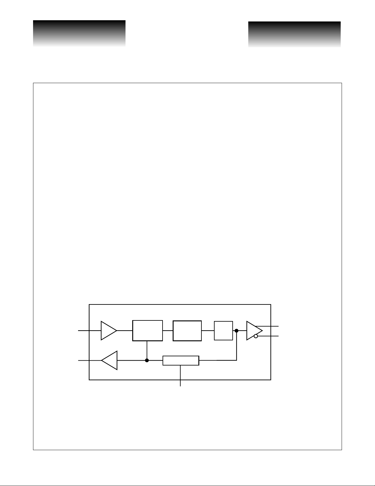
The VSC8121 is a monolithic Phase Locked Loop (PLL) based clock generator designed for telecommunications systems operating at 2.5Gb /s. The VSC 8121 inco rporates a reactanc e-based (LC) Voltage Contr olled
Oscillator (VCO) with low phase noise. The PLL’s loop filter is on-chip.
The device has a differential 2.488GHz CML clock output (CO/CON) signal, a single-ended TTL lowspeed clock (LSCLK) output equivalent in frequency to that of the reference clock, and a TTL reference clock
input selectable for 51.84MHz, 77.76MHz or 155.52MHz. TTL inputs REFSEL[0:1] are used to make this
selection.
A clean REFCLK signal is required since jitter below the PLL loop bandwidth, which is present on the
REFCLK input, will appear on the output. Jitter on REFCLK at frequencies above the loop bandwidth will be
attenuated by the PLL. The state of REFSEL[0:1] will select which frequency is expected on the REFCLK
input.
VSC8121 Functional Block Diagram
REFCLK
LSCLK
G52163-0, Rev 4.2 Page 1
04/16/01
© VITESSE SEMICONDUCTOR CORPORATION • 741 Calle Plano • Camarillo, CA 93012
Tel: (800) VITESSE • FAX: (805) 987-5896 • Email: prodinfo@vitesse.com
Ph.Freq.
Detector
Loop
Filter
Divider
REFSEL[0:1]
Internet: www.vitesse.com
VCO
CO
CON
CLOCK
OUT

VITESSE
SEMICONDUCTOR CORPORATION
2.488GHz SONET/SD H
Clock Generator
Data Sheet
VSC8121
Applications Information
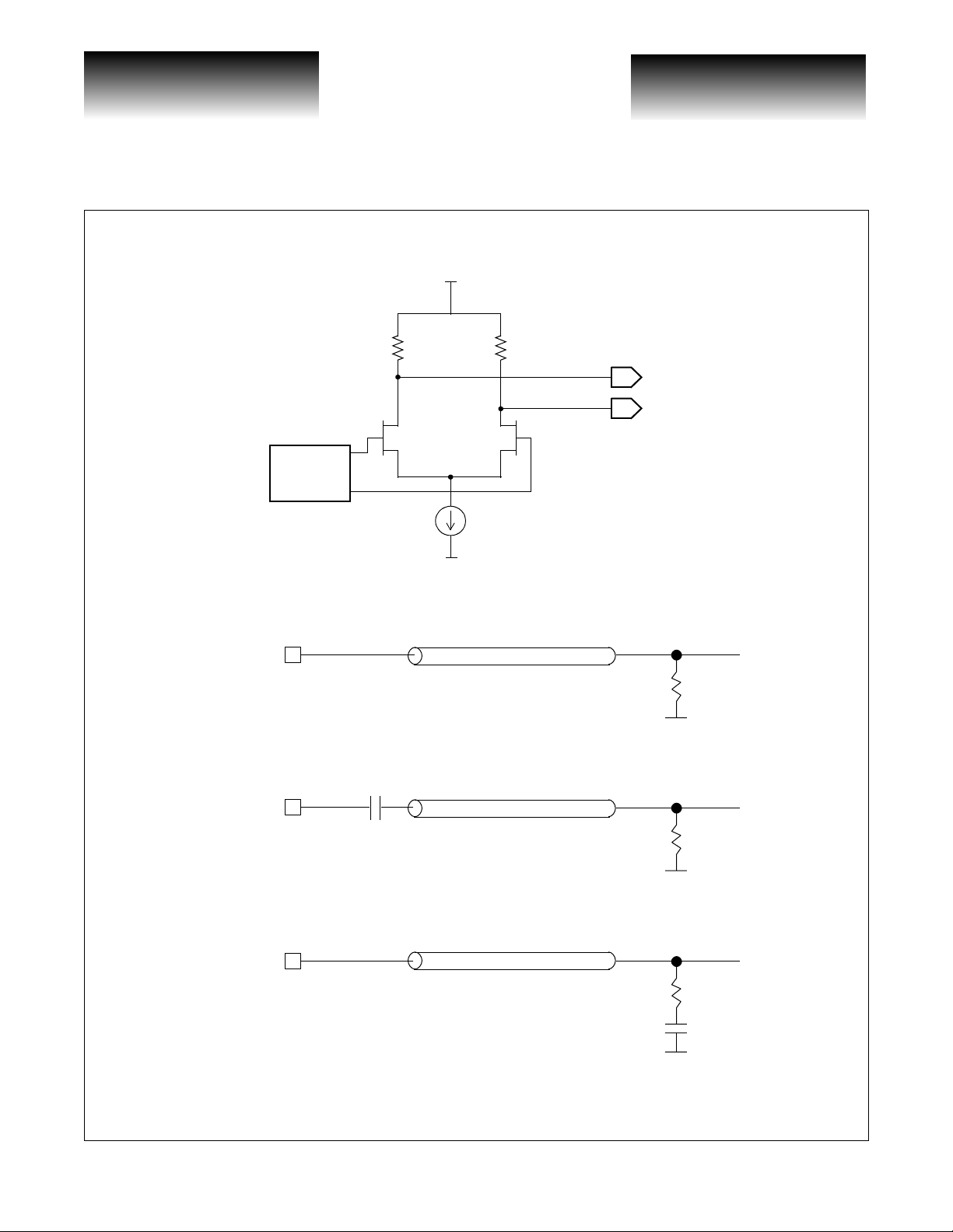
High-Speed Clock Output
The differentia l cloc k outp ut waveforms p roduce d by t he VSC8121 ar e sin usoidal i n natu re, by design. This
typically results in less n oise gener ation t han square pu lses in most cu stomer applicat ions. Fi gure 1 shows a t ypical, single-ended clock output waveform produced by the device.
Figure 1: Typical Clock Output (CO) Waveform
75mV/div
100ps/div
CO and CON are high-speed CML outp uts. As sho wn in Figu re 2, the ou tput dri ver consist s of a dif fe rential
pair designed to drive a 50
50
Ω on-chip to prevent reflections.
Careful layout of these signals is required for optimal performance. Figure 3 demonstrates various termination methods that may be employed, depending on the particular application. Either DC-coupling (termination
#1 in Figure 3) or one of two AC coupling methods (terminati ons #2 and #3) may be used. As indicate d, Vitesse
recommends termination #2 for AC-coupling.
Ω transmission line environment. Note that the output driver is back terminated to
Page 2 G52163-0, Rev 4.2
© VITESSE SEMICONDUCTOR CORPORATION • 741 Ca l le Pl an o • Camarillo, CA 93012
Tel: (800) VITESSE • FAX: (805) 987-5896 • Email: prodinfo@vitesse.com
Internet: www.vitesse.com
04/16/01
VITESSE
SEMICONDUCTOR CORPORATION
Data Sheet
VSC8121
Figure 2: High-Speed Clock Output Diagram
V
CC
50Ω
Pre-Driver
50Ω
V
EE
2.488GHz SONET/SDH
Clock Generator
CO
CON
1)
CO/CON
2)
CO/CON
3)
CO/CON
Figure 3: Example High-Speed CML Clock Output Terminations
(Recommended for DC-Coupling)
VCC
0.01 µf
V
TERM
V
50 Ω
50 Ω
TERM
(Recommended for AC-Coupling)
(Alternative for AC-Coupling)
50 Ω
0.01 µf
G52163-0, Rev 4.2 Page 3
04/16/01
© VITESSE SEMICONDUCTOR CORPORATION • 741 Calle Plano • Camarillo, CA 93012
Tel: (800) VITESSE • FAX: (805) 987-5896 • Email: prodinfo@vitesse.com
Internet: www.vitesse.com

VITESSE
SEMICONDUCTOR CORPORATION
2.488GHz SONET/SD H
Clock Generator
Reference Clock Input
The input stage at the REFCLK input pin consists of ESD protection, followed by a current limiting circuit
which precedes a driver responsible for providing the signal to the phase frequency detector. As pictured below
in Figure 4, the driver has a high impedance, FET gate input. The additional resistance contributed by the current limiting circuit is relatively negligi ble.
Figure 4: Reference Clock Input Diagram
VCC
REFCLK
VEE
Current
Limiting
VTT
Data Sheet
VSC8121
Care should be taken in selection of the reference clock. Time jitter on the reference clock which is within
the PLL’s loop bandwidth will appear on the 2.5G Hz output. Telecom quality crystal oscillators from vendors
such as Connor-Winfield or Vectron are suitable.
Table 1: Reference Clock Selection
REFSEL[1] REFSEL[0]
0 0 51.84MHz 2500KHz
1 0 77.76MHz 3000KHz
Don’t Care 1 155.52MHz 5500KHz
Die Usage
Vitesse optionally provides this device in unpackaged, die-only format for multi-chip module and related
applications. For further informtion, please contact Vitesse.
Selected Reference
Frequency
Typical
Loop Bandwidth
Page 4 G52163-0, Rev 4.2
© VITESSE SEMICONDUCTOR CORPORATION • 741 Ca l le Pl an o • Camarillo, CA 93012
Tel: (800) VITESSE • FAX: (805) 987-5896 • Email: prodinfo@vitesse.com
Internet: www.vitesse.com
04/16/01

VITESSE
SEMICONDUCTOR CORPORATION
Data Sheet
VSC8121
2.488GHz SONET/SDH
Clock Generator
AC Characteristics
T a ble 2: AC Characteristics
Parameter Description Min Typ Max Units Conditions
T
CLK
RC
d
RC
f
∆f
RC
t
jitter
NOTE: (1) ppm refers to “p arts per mi llion. ” 100 ppm (1 00/100 0000) is equ ivalen t to 0 .01%. Therefore, the equiv alen t reference
clock frequency range in MHz for +/-100ppm tolerance is as follows:
High-speed output clock period — 401.9 — ps
Reference clock duty cycle 45 — 55 %
51.84,
Reference clock frequency (selectable) —
77.76,
or
— MHz
155.52
Reference clock frequency tolerance -100 — +100 ppm
Jitter generation — 1.75 3.6 ps RMS
RC
f
X 100ppm = Acceptable Range
(1)
12kHz to 20MHz.
See Figure 5.
51.84MHz 5.184KHz 51.83MHz to 51.85MHz
77.76MHz 7.776KHz 77.75MHz to 77.78MHz
155.52MHz 15.552KHz 155.51MHz to 155.54MHz
Note that +/-100ppm tolerance for reference clock frequency more than accommodates the SONET/SDH requirement that refer-
ence clock-supplying crystals function at +/-20ppm.)
Figure 5: RMS/Peak-to-Peak Jitter (12kHz - 20MHz), REF_CLK freq = 77.76MHz
3.0
2.5
2.0
1.5
ps
1.0
0.5
0.0
0
RMS Jitter Pk-Pk Jitter
25
20
15
ps
10
5
20 40
Case Temperature (deg C)
100
80
60
0
0
20 40
Case Temperature (deg C)
60
100
80
G52163-0, Rev 4.2 Page 5
04/16/01
© VITESSE SEMICONDUCTOR CORPORATION • 741 Calle Plano • Camarillo, CA 93012
Tel: (800) VITESSE • FAX: (805) 987-5896 • Email: prodinfo@vitesse.com
Internet: www.vitesse.com

VITESSE
SEMICONDUCTOR CORPORATION
2.488GHz SONET/SD H
Clock Generator
DC Characteristics
T able 3: Low Speed I/O
Parameter Description Min Typ Max Units Conditions
V
OH
V
OL
V
IH
V
IL
I
IH
I
IL
T able 4: High-Speed Differential Outputs
Parameter Description Min Typ Max Units Conditions
V
OD
V
OCM
Note: Output jitter characteristics apply for differential outputs.
Output HIGH voltage (TTL) 2.4 ——VIOH = -1.0 mA
Output LOW voltage (TTL) ——0.5 V IOL = +1.0 mA
Input HIGH voltage (TTL) 2.0 — 3.47 V —
Input LOW voltage (TTL) 0 — 0.8 V —
Input HIGH current (TTL) — 50 500 µAVIN = 2.4V
Input LOW current (TTL) ——-500 µAVIN = 0.5V
Output differential voltage 450 — 800 mV
Output common-mod e voltage
V
0.40
V
0.80
V
0.80
CC
CC
CC
-
—
-
—
-
—
V
0.25
V
0.50
V
0.50
CC
CC
CC
mV
mV
mV
T e r mi na tio n #1
(See Figure 3)
T e r mi na tio n #2
(See Figure 3)
T e r mi na tio n #3
(See Figure 3)
Data Sheet
VSC8121
Table 5: Power Supply Currents
Parameter Description Min Typ Max Units Conditions
I
CC
P
D
Power supply current from V
Power dissipation 0.7 W Outputs Open
CC
200 mA Outputs Open
Page 6 G52163-0, Rev 4.2
© VITESSE SEMICONDUCTOR CORPORATION • 741 Ca l le Pl an o • Camarillo, CA 93012
Tel: (800) VITESSE • FAX: (805) 987-5896 • Email: prodinfo@vitesse.com
Internet: www.vitesse.com
04/16/01
 Loading...