

VITESSE VSC8117QP2, VSC8117QP1, VSC8117QP Datasheet

VITESSE
SEMICONDUCTOR CORPORATION
Data Sheet
SC8117
ATM/SONET/SDH 622/155 Mb/s Transceiver Mux/Demux
with Integrated Clock Generation and Clock Recovery
Features
• Operates at Either STS-3/STM-1 (155.52Mb/s)
or STS-12/STM-4 (622.08Mb/s) Data Rates
• Compatible with Industry ATM UNI Devices
• On Chip Clock Generation of the
622.08MHz High Speed Clock (Mux)
or
• On Chip Clock Recovery of the
622.08MHz High Speed Clock (Demux)
• 8 Bit Parallel TTL Interface
• SONET/SDH Frame Recovery
• Loss of Signal (LOS) Input & LOS Detection
155.52MHz
155.52MHz or
• +3.3V/5V programmable PECL Serial Interface
• Provides Equipment, Facilities and Split Loopback Modes as well as Loop Timing Mode
• Provides TTL and PECL reference clock inputs
• Meets Bellcore, ITU and ANSI Specifications for
Jitter Performance
• Low Power - 1.0 Watts Typical
• 64 PQFP Package
General Description
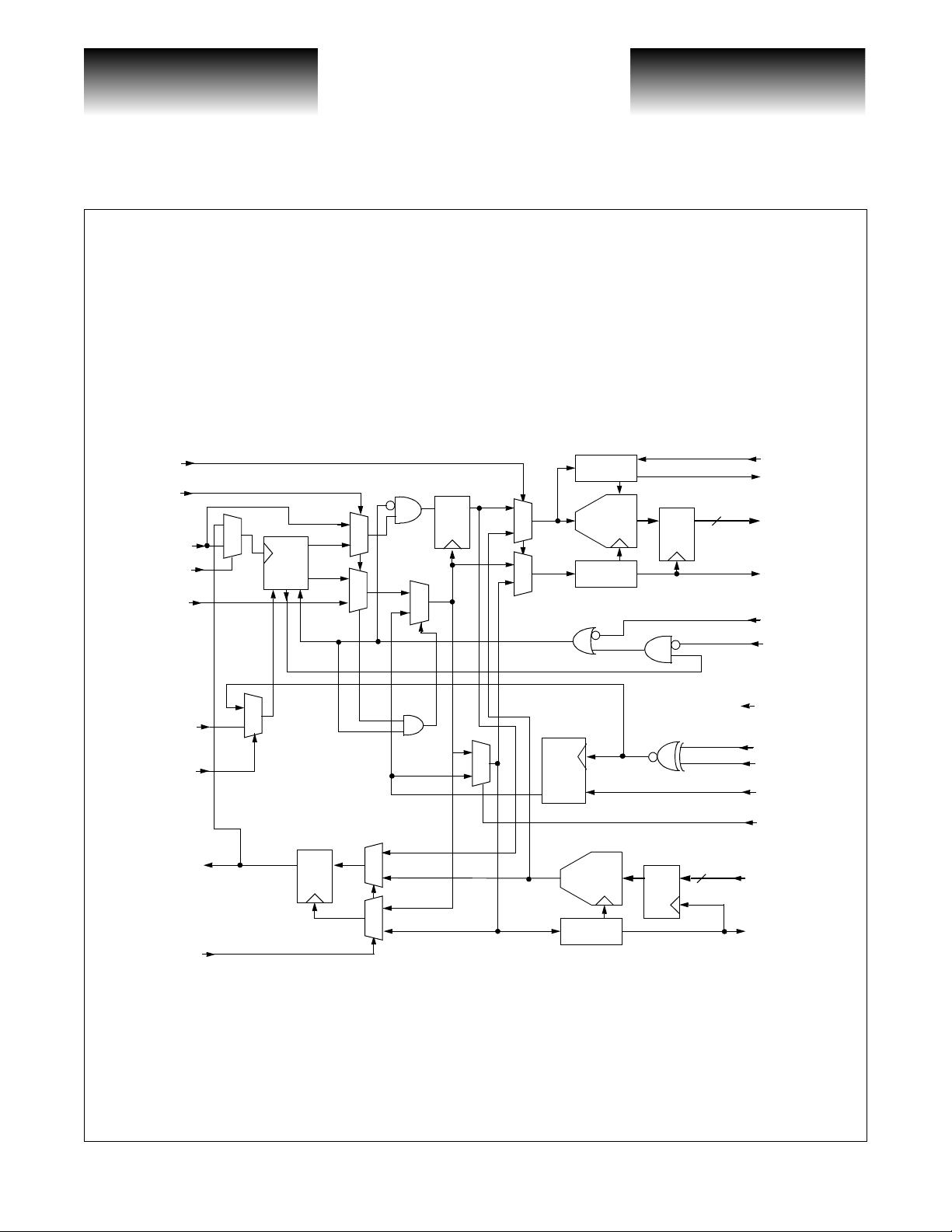
The VSC8117 is an ATM/SONET/SDH compatible transceiver integrating an on-chip Clock Multiplication
Unit (PLL) for the high speed clock as well as a clock and data recovery unit (CRU) with 8 bit serial-to-parallel
and parallel-to-serial data conversion. The PLL clock is used for serialization in the transmit direction (Mux).
The recovered clock is used for deserializatio n in the receive direction (Demux). Th e demultiplexer contains
SONET/SDH frame detection and recovery. The device provides facility loopback, equipment loopba ck, and
loop timing modes. The part is packaged in a 64-pin PQFP with integrated heat spreader for optimum thermal
performance and reduced cost. The VSC81 17 provides an integrated solution for ATM physical layers and
SONET/SDH systems applications.
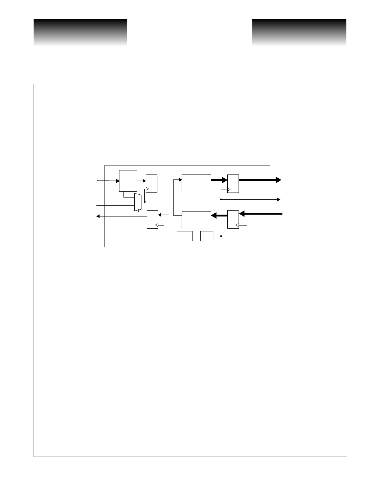
Functional Description
The VSC8117 is designed to provide a SONET/SDH compliant interface between the high spee d optical
networks and the lower speed User Network Interface devices such as the PM5355 S/UNI-622. The VSC8117
converts 8 bit parallel data at 77.76Mb/s or 19.44Mb/s to a serial bit str eam at 622.08Mb/s or 15 5.52Mb/s
respectively. The device also provides a Facility Loopback function which loops the received high speed data
and clock (optionally recovered on-chip) directly to the high speed trans mit outpu ts. A Cloc k Multiplier Unit
(CMU) is integrated into the transmit circuit to generate the high speed clock for the serial output data stream
from input reference fr equenci es of 19. 44 or 7 7.76 MHz. Th e CMU can be byp assed with th e reco v ered clo ck in
loop timing mode thus synchronizing the entire part to a single clock. The block diagram on page 2 shows the
major functional blocks associated with the VSC8117.
The receiv e sect io n pr ovides the serial-to-par al l el conversion , conver t in g the 155.52Mb/s or 622.08Mb /s bit
stream to an 8 bit parallel o utput at 19 .44Mb/s or 77.76Mb /s respectively. A Clock Reco v ery Unit (CRU) is integrated into the receive circuit to recover the high speed clock from the received serial data stream. The receive
section provides an Equipment Loopback function which will loop the low speed transmit data and clock back
through the receive section to the 8 bit parallel data bus and clock outputs. The VSC8117 also provides the
option of selecting between either its internal CRU’s recovered clock and data signals or optics containing a
G52221-0, Rev. 4.1
1/8/00 741 Calle Plano, Camarillo, CA 93012 • 805/388-3700 • FAX: 805/987-5896
VITESSE SEMICONDUCTOR CORPORATION
Page 1
VITESSE
SEMICONDUCTOR CORPORATION
ATM/SONET/SDH 622/155 Mb/s Transceiver Mux/Demux
with Integrated Clock Generation and Clock Recovery
Data Sheet
VSC8117
CRU clock and data signals. (In this mode the VSC8117 operates just like the VSC8111 and VSC8116). The
receive section al so contains a SONET/ SDH frame detector circuit which is used to pro vide frame plus es during
the A1, A2 boundary in the serial to parallel converter. This only occurs when OOF is high. Both internal and
external LOS functions ar e supp or te d. The high speed serial signals can be made PECL compatibl e or LVPECL
compatible by setting the proper voltage on the V
supply pins
DDP
VSC8117 Block Diagram
EQULOOP
DSBLCRU
RXDATAIN+/-
CRUEQLP
RXCLKIN+/-
FRAMER
DQ
0
1
REC-CLK
1
0
0
1
1
0
REC-DATA
CRU
losdet
0
1
0
1
1:8
DEMUX
Divide-by-8
DQ
8
OOF
FP
RXOUT[7:0]
RXLSCKOUT
LOSPECL
LOSDETEN_
CRUREFCLK
CRUREFSEL
TXDATAOUT+/-
FACLOOP
0
1
1
0
DQ
1
0
1
0
CMU
MUX
Divide-by-8
8:1
QD
8
STS12
REFCLKP+/REFCLK
CMUFREQSEL
LOOPTIM0
TXIN[7:0]
TXLSCKOUT
Page 2
741 Calle Plano, Camarillo, CA 93012 • 805/388-3700 • FAX: 805/987-5896 1/8/00
VITESSE SEMICONDUCTOR CORPORATION
G52221-0, Rev 4.1
VITESSE
SEMICONDUCTOR CORPORATION
Data Sheet
SC8117
Transmit Section
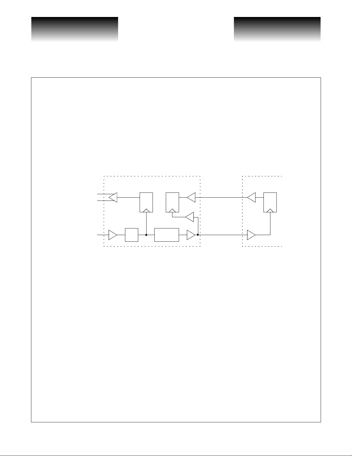
Byte-wide data is presented to TXIN[7:0] and is clocked into the part on the rising edge of TXLSCKOUT.
TXLSCKOUT also latches TXIN[7:0] into the part as shown in Figure 1. The data is then serialized (MSB leading) and presented at the TXD ATA OUT+/- pins. The seria l outp ut stream is synchron ized t o the CMU generated
clock which is a phase locked and frequency scaled version of the input reference clock. External control inputs
CMUFREQSEL and STS-12 select the multiply ratio of the CMU for either STS-3 (155MbS) or STS-12
(622Mb/s) transmission (see Table 10). A divide-by-8 version of the CMU clock (TXLSCKOUT) should be
used to synchronize the transmit interface of the UNI device to the transmit input registers on the VSC8117.
Figure 1: Data and Clock Transmit Block Diagram
TXDATAOUT+
TXDATAOUT-
ATM/SONET/SDH 622/155 Mb/s Transceiver Mux/Demux
with Integrated Clock Generation and Clock Recovery
VSC8117 PM5355
DQDQ
TXIN[7:0]
TXLSCKIN
DQ
REFCLK
Receive Section
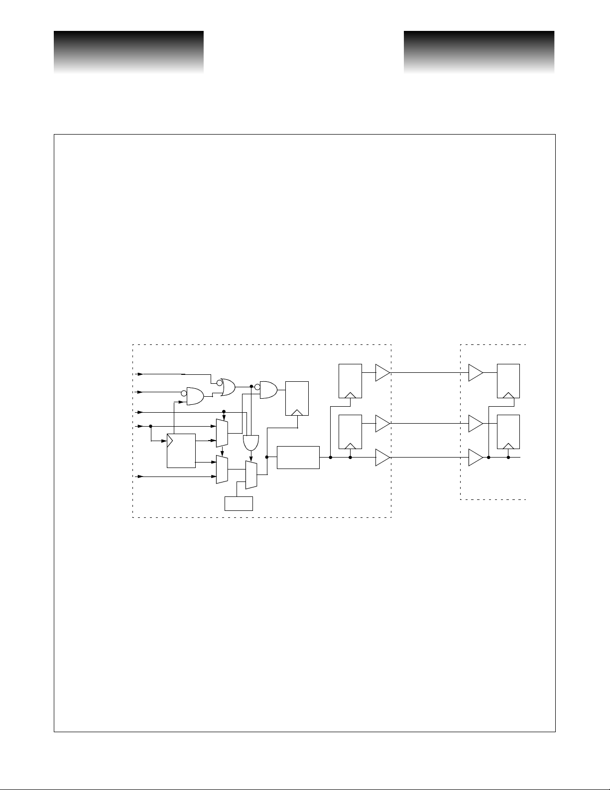
High speed Non-Return to Zero (NRZ) serial data at 155Mb/s or 622Mb/s are received by the RXDATAIN
inputs. The CRU recovers the high speed clock from the serial data input. The serial data is converted to bytewide parallel data and presented on RXOUT[7:0] pins. A divide-by-8 version of the high-speed clock
(RXLSCKOUT) should be used to synch r onize t he byte-serial RXOUT[7:0] data with the receive portion of the
UNI device. The on-chip CRU is by-passed by setting the DSBLCRU input high. In this mode, the serial input
data and corresponding clock are received by the RXDATAIN and RXCLKIN inputs respectively. RXDATAIN
is clocked in on the rising edge of RXCLKIN+. See Figure 2.
The receive section also includes frame detection a nd recovery circuitry which detec ts the SONET/SDH
frame, aligns the received serial data on byte boundaries, and initiates a frame pulse on FP coincident with the
byte aligned data. The frame recovery is initiated when OOF is held high which must occur at lea s t 4 byte clock
cycles before the A1A2 boundary. The OOF input control is a level-sensitive signal, and th e VSC8117 will continually perform frame detection and recovery as long as this pin is held high even if 1 or more frames has been
detected. Frame detection and recovery occurs when a series of three A1 bytes followed by three A2 bytes has
been detected. The paralle l outp ut data on R XOUT[7:0] wil l be b yt e alig ned startin g on the thi rd A2 b yte. Wh en
a frame is detected, a single byte clock pe riod long pulse is g enerated o n FP which i s synchronize d with the
byte-aligned third A2 byte on RXOUT[7:0]. The frame detector sends a FP pulse only if OOF is high.
Divide-by-8CMU
TXLSCKOUT
G52221-0, Rev. 4.1
1/8/00 741 Calle Plano, Camarillo, CA 93012 • 805/388-3700 • FAX: 805/987-5896
VITESSE SEMICONDUCTOR CORPORATION
Page 3
VITESSE
SEMICONDUCTOR CORPORATION
ATM/SONET/SDH 622/155 Mb/s Transceiver Mux/Demux
with Integrated Clock Generation and Clock Recovery
Data Sheet
VSC8117
Loss of Signal
The VSC8117 features Loss of Signal (LOS) detection. Loss of Signal is declared if the incoming serial
data stream has no transition continuously for more than 128 bits. During an LOS condition, the VSC 8117
forces the receive data low which is an indication for an y do wnstre am equipment that an optical interfac e fail ure
has occurred. The receive section continues to be clocked by the CRU as it is now locked to the CRUREFCLK
unless DSBLCRU is active or CRUREFSEL is inactive in which case it will be clocked by the C MU. This LOS
condition will be removed when the part detects more than 16 transitions in a 128 bit time window. This LOS
detection feature can be disabled by applying a high level to the LOSDETEN_ input. The VSC8117 also has a
PECL input LOSPECL to force the part into a Loss of Signal stat e. Most optics have a PECL outpu t usually
called “SD” or “FLA G” indi catin g a lack of or presence of optica l po wer. Depending on the optics manufacturer
this signal is either active high or active low. The LOSPECL input on the VSC8117 is active low.
Figure 2: Data and Clock Receive Block Diagram
PM5355
LOSPECL
LOSDETEN_
VSC8117
DQ
DQ
RXOUT[7:0]
DQ
DSBLCRU
RXDATAIN+/-
RXCLKIN+/-
CRU
1
0
0
0
1
1
CMU
Divide-by-8
DQ
FP
RXLSCKOUT
DQ
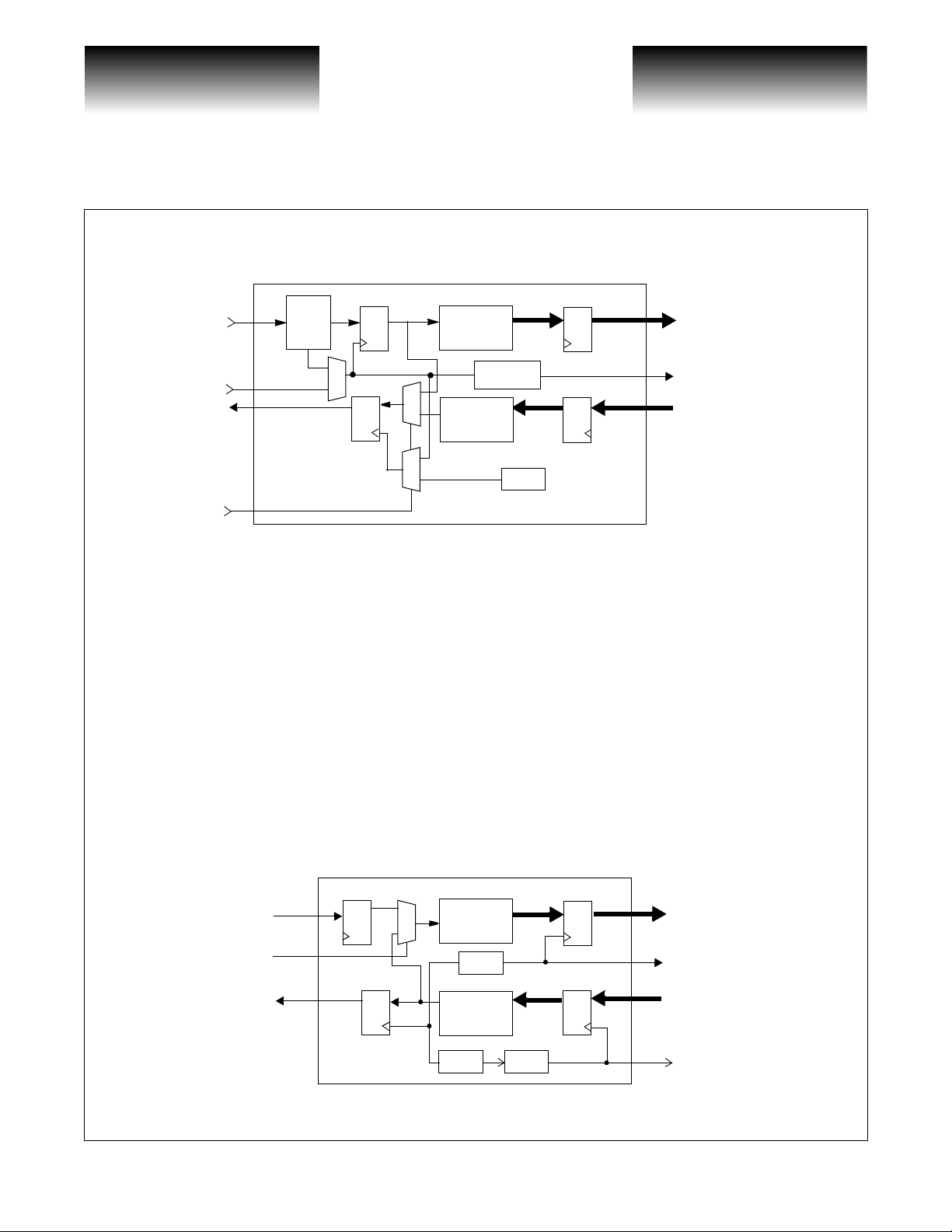
Facility Loopback
The Facility Loopback function is controlled by the FACLOOP signal. When the FACLOOP signal is set
high, the Facility Loopback mode is activated and the high speed serial receive data (RXDATAIN) is presented
to the high speed transmit output (TXDATAOUT). See Figure 3. In Facility Loopback mode the high speed
receive data (RXDATAIN) is also converted to parallel data and presented to the low speed receive data output
pins (RXOUT[7:0]). The receive clock (RXCLKIN) or the recovered clock is also divided down and presented
to the low speed clock output (RXLSCKOUT).
Page 4
741 Calle Plano, Camarillo, CA 93012 • 805/388-3700 • FAX: 805/987-5896 1/8/00
VITESSE SEMICONDUCTOR CORPORATION
G52221-0, Rev 4.1
VITESSE
SEMICONDUCTOR CORPORATION
Data Sheet
SC8117
ATM/SONET/SDH 622/155 Mb/s Transceiver Mux/Demux
with Integrated Clock Generation and Clock Recovery
Figure 3: Facility Loopback Data Path
RXDATAIN
RXCLKIN
TXDATAOUT
FACLOOP
Recovered
Clock
CRU
Q
0
1
Q
1
D
0
1
0
1:8
Serial to
Parallel
Divide-by-8
Parallel to
Serial
PLL
D
Q
Q
D
RXOUT[7:0]
RXLSCKOUT
TXIN[7:0]8:1
D
Equipment Loopback
The Equipment Loopback function is controlled by the EQULOOP signal. When the EQULOOP signal is
set high, the Equipment Loopback mode is activated and the high speed transmit data generated from the parallel to serial conversion of the low speed data (TXIN[7:0]) is selected and converted back to parallel data in the
receiver section and presented to the low speed parallel o utputs (RXOUT[7:0]). S ee Figure 4. The inte rnally
generated 155/622MHz clock i s used t o g enerate t he low speed receive clock output (RXLSCKOUT). In Equipment Loopback mode the transmit data (TXIN[7:0]) is serialized by the on-chip CMU and presente d at the hi gh
speed output (TXDATAOUT).
CRU Equipment Loopback
Exactly the same as equipment loopback, the point where the transmit data is looped back is moved all the
way back to the high speed I/O. When the CRUEQLP signal is set high, transmit data is looped back to the
CRU, replacing RXDATAIN±
Figure 4: Equipment Loopback Data Path
D
RXDATAIN
EQULOOP
TXDATAOUT
G52221-0, Rev. 4.1
Q
0
1
Q
D
VITESSE SEMICONDUCTOR CORPORATION
1:8
Serial to
Parallel
8
÷
8:1
Parallel to
Serial
PLL ÷ 8
1/8/00 741 Calle Plano, Camarillo, CA 93012 • 805/388-3700 • FAX: 805/987-5896
D
Q
Q
D
RXOUT[7:0]
RXLSCKOUT
TXIN[7:0]
TXLSCKOUT
Page 5
VITESSE
SEMICONDUCTOR CORPORATION
ATM/SONET/SDH 622/155 Mb/s Transceiver Mux/Demux
with Integrated Clock Generation and Clock Recovery
Data Sheet
VSC8117
Split Loopback
Equipment and facility loopback modes can be enabled simultaneously. In this case, high-speed serial data
received (RXDATAIN) is mux’d through to the high-speed serial output (TXDATAOUT). The low-speed transmit byte wide bus(TXIN[7:0]) and (TXLSCKIN) are mux’d into the low-speed byte wide receive output bus
(RXOUT[7:0]) and (RXLSCKOUT). See Figure 5.
Figure 5: Split Loopback Datapath
D
RXDATAIN
RXCLKIN
DSBLCRU
TXDATAOUT
Recovered
Clock
CRU
Q
0
1
Q
D
PLL
1:8
Serial to
Parallel
8:1
Parallel to
Serial
÷8
D
Q
Q
D
RXOUT[7:0]
RXLSCKOUT
TXIN[7:0]
TXLSCKIN
Loop Timing
LOOPTIM0 mode bypasses the CMU when the LOOPTIM0 input is asserted high. In this mode the CMU
is bypassed by using the receive clock (RXCLKIN), and the entire part is synchronously clocked from a single
external source.
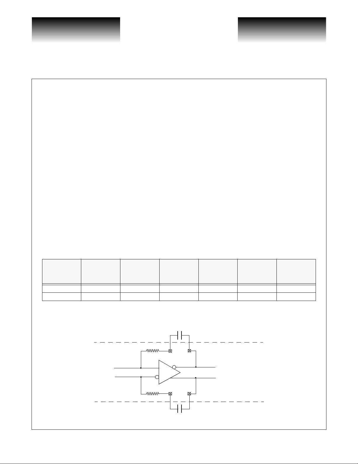
Clock Synthesis
The VSC8117 uses an integrated phase-locked loop (PLL) for c lock synthesis of the 622MHz hig h speed
clock used for serialization in the transmitter section. The PLL is comprised of a phase-frequency detector
(PFD), an integrating operation amplifier and a voltage controlled oscillator (VCO) configured in classic feedback system. The PFD compares the selected divided down version of the 622MHz VCO (pin CMUFREQSEL
selects the divide-by ratios of 8 or 32, see Table 10) and the reference clock. The integrator provides a transfer
function between input phase error and ou tput voltage control. The V CO portion of the PLL is a voltage controlled ring-oscillator with a center frequency of 622MHz.
The reactive elements of the integrator are located off-chip and are connected to the feedback loop of the
amplifier through the CP1, CP2, CN1 and CN2 p ins. The configuration of thes e external surface moun ted
capacitors is shown in Figure 6. Table 1 shows the recommended external capacitor values for the configurable
reference frequencies.
Page 6
741 Calle Plano, Camarillo, CA 93012 • 805/388-3700 • FAX: 805/987-5896 1/8/00
VITESSE SEMICONDUCTOR CORPORATION
G52221-0, Rev 4.1
VITESSE
SEMICONDUCTOR CORPORATION
Data Sheet
SC8117
Good analog design practices should be applied to the board design for these external components. Tightly
controlled analog ground and power planes should be provided for the PLL portion of the circuitry. The dedicated PLL power (VDDA) and ground (VSSA) pins should have quiet supply planes to minimize jitter generation within the clock synthesis uni t. This is accomp lished by eithe r using a ferrite be ad or a C-L-C choke (
filter) on the (VDDA) power pins. Note: Vitesse recommends a (π filter) C-L-C choke over using a ferrite bead.
All ground planes should be tied together using multiple vias.
Reference Clocks
To improve jitter performance and to provide flexibility, an additional differential PECL reference clock
input is provided. This reference clock is internally XNOR’d with a TTL reference clock input to generate the
reference for the CMU. Vitesse reco mmends u s ing t he di fferential PECL i nput and tieing the unused TTL r efer ence clock low. If the TTL reference clock is used the positive side of the differential PECL reference clock
“REFCLKP+” should be tied to ground. “REFCLKP+/-” are internally biased with on-chip resistors to 1.65(for
3.3V case) volts, see figure 13 for schematic of internal biasing of differential I/O’s.
The CRU has the option of either using the CMU’s reference clock or its own independent reference clock
“CRUREFCLK”. This is accomp lished wit h the control signal “CRUREFSEL”. The “CR UREFCLK” should be
used if the system is being o perated in e ither a regeneration or looptiming m ode. In e ither of the se modes the
quality of the “CRUREFCLK” is not a concern, thus it can be driven by a simple 77.76MHz crystal, the key is
its’ independent of the CMU’s reference clock.
ATM/SONET/SDH 622/155 Mb/s Transceiver Mux/Demux
with Integrated Clock Generation and Clock Recovery
π
Table 1: Recommended External Capacitor Values
Reference
Frequency
[MHz]
19.44 32 0.1 0.1 X7R 0603/0805 +/-10%
77.76 8 0.1 0.1 X7R 0603/0805 +/-10%
Divide Ratio CP CN Type Size Tol.
Figure 6: External Integrator Capacitor
CP = 0.1 µF
CP1
+
-
CN1 CN2
CP2
CN = 0.1 µF
G52221-0, Rev. 4.1
1/8/00 741 Calle Plano, Camarillo, CA 93012 • 805/388-3700 • FAX: 805/987-5896
VITESSE SEMICONDUCTOR CORPORATION
Page 7
 Loading...