

VITESSE VSC8116QP2, VSC8116QP1, VSC8116QP Datasheet
VITESSE
SEMICONDUCTOR CORPORATION
Data Sheet
SC8116
ATM/SONET/SDH 622/155Mb/s Transceiver
Mux/Demux with Integrated Clock Generation
Features
• Operates at Either STS-3/STM-1 (155.52 Mb/s) or
STS-12/STM-4 (622.08 Mb/s) Data Rates
• Compatible with Industry ATM UNI Devices
• On Chip Clock Generation of the 155.52 Mhz
or 622.08 Mhz High Speed Clock
• Dual 8 Bit Parallel TTL Interface
• SONET/SDH Frame Detection and Recovery
• Loss of Signal (LOS) Control
• Provides Equipment, Facilities and Split Loopback Modes as well as Loop Timing Mode
• Meets Bellcore, ITU and ANSI Specifications for
Jitter Performance
• Single 3.3V Supply Voltage
• Low Power - 1.2 Watts Maximum
• 64 PQFP Package
General Description
The VSC8116 is an ATM/SONET/SDH compatible transceiver integrating an on-chip clock multiplication
unit (PLL) for the high speed clock and 8 bit serial-to-parallel and parallel-to-serial data conversion. The high
speed clock generated by the on-chip PLL is selectable for 155.52 or 622.08 MHz operation. The demultiplexer
contains SONET/SDH frame detection and recovery. In addition, the device provides both facility and equipment loopback modes and loop timing modes. The part is packaged in a 64 PQFP with an integrated heat
spreader for optimum thermal performance and reduced cost. The VSC8116 provides an integrated solution for
ATM physical layers and SONET/SDH systems applications.
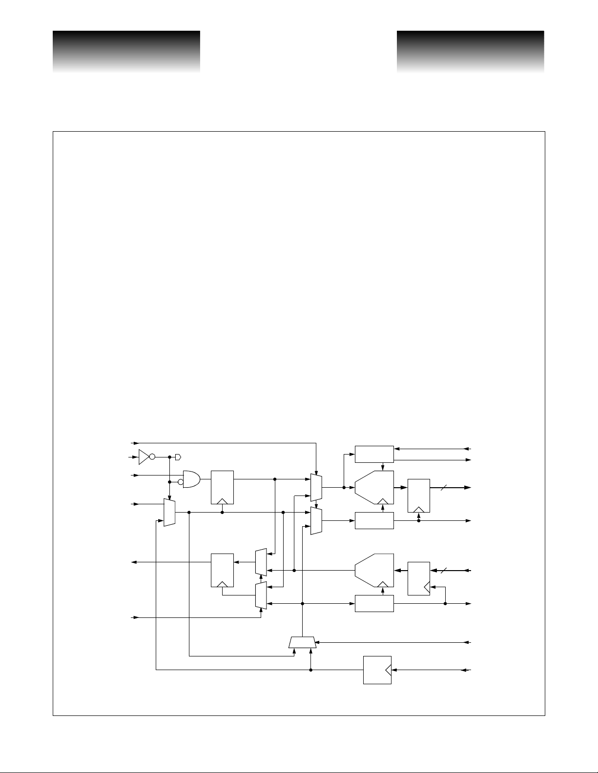
VSC8116 Block Diagram
EQULOOP
LOSTTL
RXDATAIN+/-
RXCLKIN+/-
TXDATAOUT+/-
FACLOOP
LOS
DQ
0
1
FRAMER
0
1
0
1
DQ
1
0
1
0
01
1:8
DEMUX
Divide-by-8
8:1
MUX
Divide-by-8
CMU
DQ
QD
8
8
OOF
FP
RXOUT[7:0]
RXLSCKOUT
TXIN[7:0]
TXLSCKOUT
LOOPTIM0
REFCLK
G52220-0, Rev 4.1
1/8/00 741 Calle Plano, Camarillo, CA 93012 • 805/388-3700 • FAX: 805/987-5896
VITESSE SEMICONDUCTOR CORPORATION
Page 1
VITESSE
SEMICONDUCTOR CORPORATION
ATM/SONET/SDH 622/155Mb/s Transceiver
Mux/Demux with Integrated Clock Generation
Data Sheet
VSC8116
Functional Description
The VSC8116 is designed to provide a SONET/SDH compliant interface between the high spee d optical
networks and the lower speed User Network Interface (UNI) devices such as the PM5355 S/UNI-622 (or
PM5312 STTX). The VSC8116 transmit section converts 8 bit parallel data at 77.76 Mb/s or 19.44 Mb/s to a
serial bit stream at 622.08 Mb/s or 155.52 Mb/s, respectively. It also provides a Facility Loopback function
which loops the received high speed data and c lock directly to the transmit outp uts. A Clock Multiplier Un it
(CMU) is integrated into the transmit circuit to generate the high speed clock for the serial output data stream
from input references frequency of 19.44 or 77.76 MHz. The CMU can be bypassed by using the receive clock
in loop timing mode thus synchronizing the entire part to a single clock (RXCLKIN).
The receive section provides the serial-to-parallel conversion, converting 155 Mb/s or 622 Mb/s to an 8 bit
parallel output at 19.44 Mb/ s or 77.76 Mb /s, r esp ect ively. The receive section provides an Equipment Lo opb ack
function which will loop the low speed transmit data and clock ba ck th ro ugh the receive section to t he 8 bit parallel data bus and clock outputs. The receive section also contains a SONET/SDH frame detector circuit which
is used to provide frame recovery in the serial to parallel converter. The block diagram on page 1 shows the
major functional blocks associated with the VSC8116.
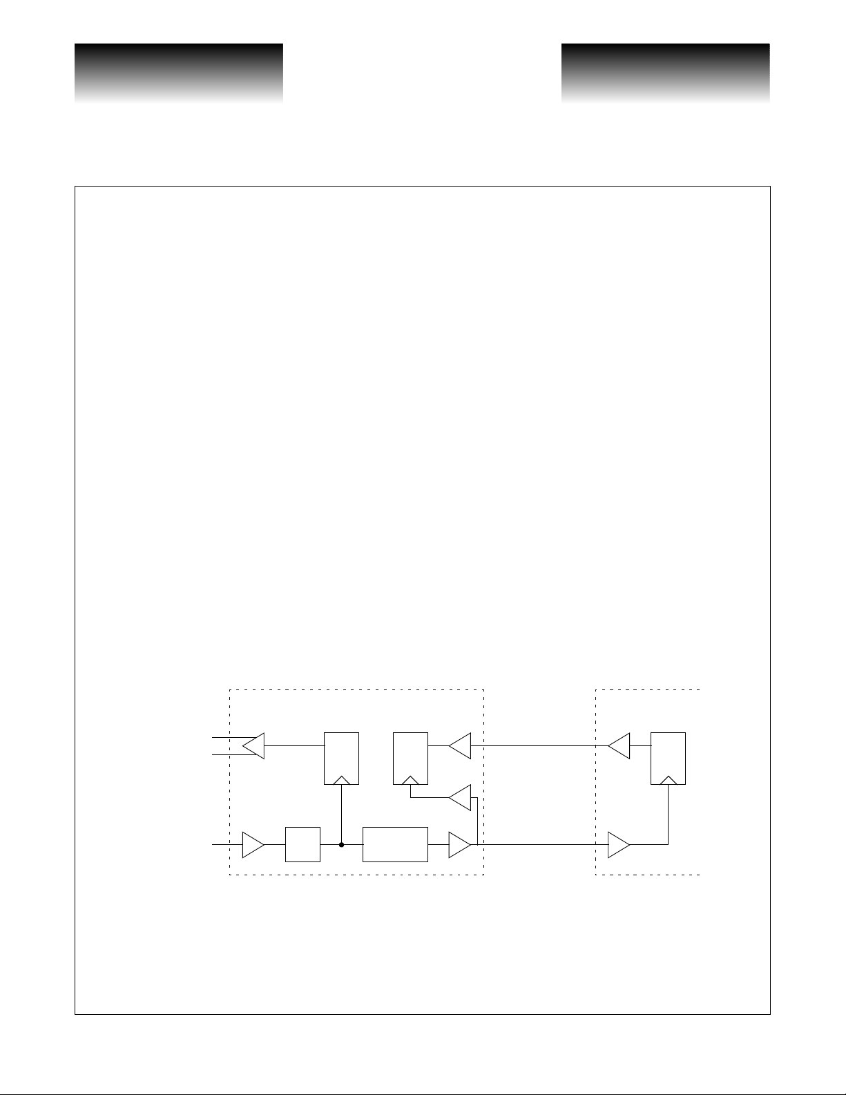
Transmit Section
Byte-wide data is prese nted to TX IN [7 :0] a nd is c locked i nto the p art o n th e risi ng ed ge of TXL SC KOUT
(refer to Figure 1). The data is then serialized (MSB leading) and presented at the TXDATAOUT+/- pins. The
serial output stream is synchronized to the CMU generated clock which is a phase locked and frequency scaled
version of the input reference clock. External control inputs CMUFREQSEL and STS12 select the multiply
ratio of the CMU and either STS-3 (155 Mb/s) or STS-12 (622 Mb/s) transmission (See Table 2).
Figure 1: Data and Clock Transmit Block Diagram
TXDATAOUT+
TXDATAOUT-
REFCLK
Page 2
741 Calle Plano, Camarillo, CA 93012 • 805/388-3700 • FAX: 805/987-5896 1/8/00
VSC8116 PM5355
DQDQ
Divide-by-8CMU
VITESSE SEMICONDUCTOR CORPORATION
TXIN[7:0]
TXLSCKOUT
DQ
G52220-0, Rev 4.1
VITESSE
SEMICONDUCTOR CORPORATION
Data Sheet
SC8116
ATM/SONET/SDH 622/155Mb/s Transceiver
Mux/Demux with Integrated Clock Generation
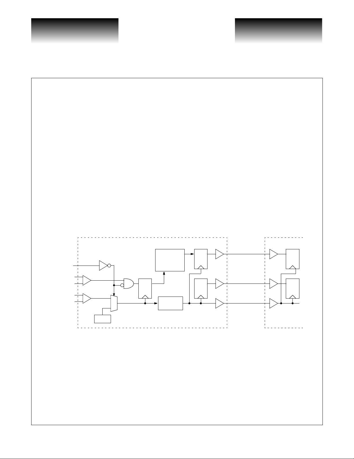
Receive Section
High speed Non-Return to Zero (NRZ) serial data at 155Mb/s or 622Mb/s are received by the RXDATAIN
inputs. The corresponding clock is received by the RXCLKIN inputs. RXDATAIN is clocked in on the rising
edge of RXCLKIN+. See Figure 2. The serial data is converted to byte-wide parallel data and presented on
RXOUT[7:0] pins. A divide-by-8 version of the high-speed clock (RXLSCKOUT) should be used to synchronize the byte-serial RXOUT[7:0] data with the receive portion of the UNI device.
The receive section also includes frame detection a nd recovery circuitry which detec ts the SONET/SDH
frame, aligns the received serial data on byte boundaries, and initiates a frame pulse on FP coincident with the
byte aligned data. The frame recovery is initiated when OOF is held high which must occur at lea s t 4 byte clock
cycles before the A1A2 boundary. The OOF input control is a level-sensitive signal, and th e VSC8116 will continually perform frame detection and recovery as long as this pin is held high even if 1 or more frames has been
detected. Frame detection and recovery occurs when a series of three A1 bytes followed by three A2 bytes has
been detected. The paralle l outp ut data on R XOUT[7:0] wil l be b yt e alig ned startin g on the thi rd A2 b yte. Wh en
a frame is detected, a single byte clock pe riod long pulse is g enerated o n FP which i s synchronize d with the
byte-aligned third A2 byte on RXOUT[7:0]. The frame detector sends an FP pulse only if OOF is high or if a
frame was detected while OOF was being pulled low.
Figure 2: Data and Clock Receive Block Diagram
PM5355
DQ
DQ
LOSTTL
RXDATAIN+
RXDATAIN-
RXCLKIN+
RXCLKIN-
CMU
VSC8116
1:8 Serial
to Parallel
0
1
Divide-by-8
DQ
DQDQ
RXOUT[7:0]
FP
RXLSCKOUT
Loss of Signal
During a LOS condition, the VSC8116 forces the receive data low which is an indication for any downstream
equipment that an optical in terface failure has occurred. The receive section is clocked by the transmit section’s
G52220-0, Rev 4.1
1/8/00 741 Calle Plano, Camarillo, CA 93012 • 805/388-3700 • FAX: 805/987-5896
VITESSE SEMICONDUCTOR CORPORATION
Page 3
VITESSE
SEMICONDUCTOR CORPORATION
ATM/SONET/SDH 622/155Mb/s Transceiver
Mux/Demux with Integrated Clock Generation
Data Sheet
VSC8116
PLL clock multiplier. Optics have either a PECL or TTL output, usually called “SD” (Signal Detect) or “FLAG”
indicating either a lack of or presence of optical power. Depending on the optics manufacture this signal is
either activ e hi gh or act ive low pol arit y. If the optics Signal Detect or FLAG output is a “TTL” signal , it shoul d
be connected to LOSTTL . If it’s a “PECL” signal it should be connected through a “P ECL” to “T TL” tran slator
(such as the Motorola “MC100ELT21”) which then drives LOSTTL. The follow on part to VSC8116 is the
VSC8117, in this device the signal LOSTTL has been changed to LOSPECL, a PECL input.
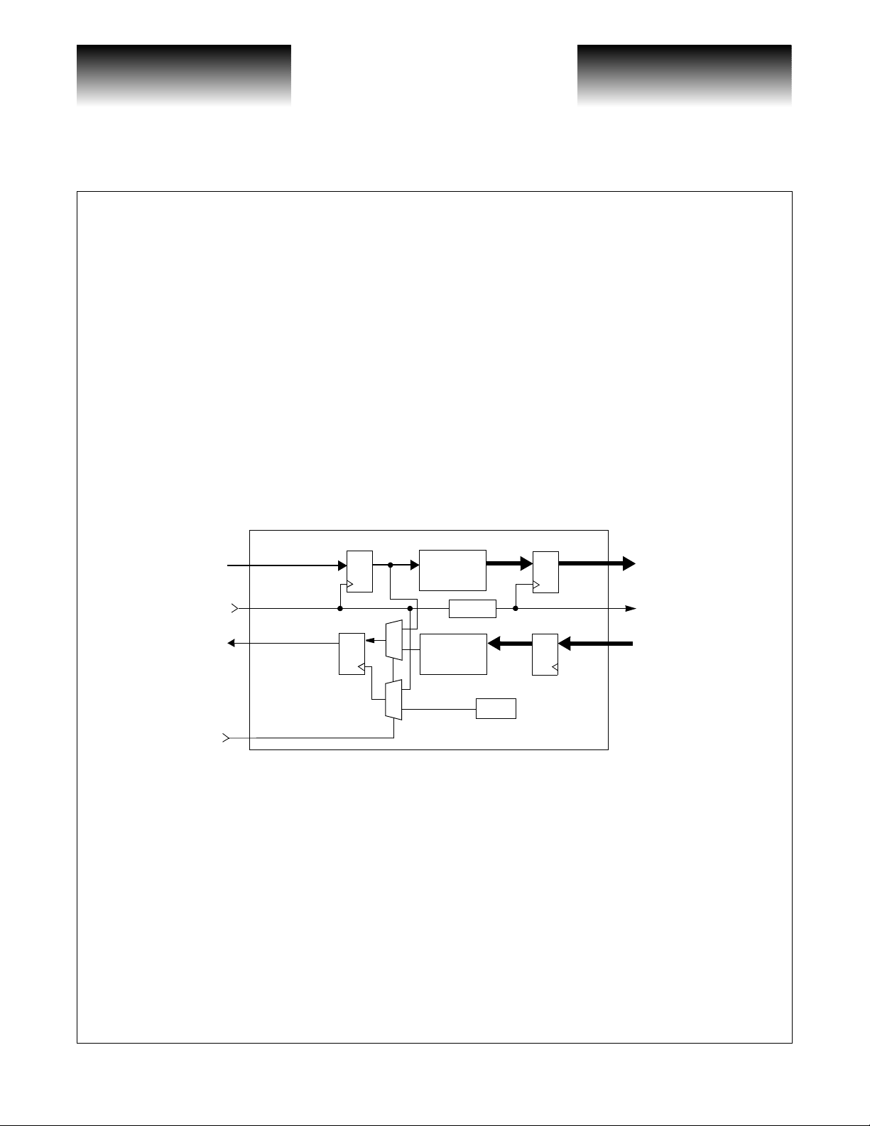
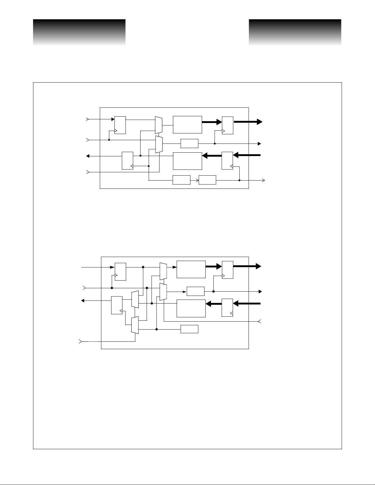
Facility Loopback
The Facility Loopback function is controlled by the FACLOOP signal. When the FACLOOP signal is set
high, the Facility Loopback mode is activated and the high speed serial receive data (RXDATAIN) is presented
at the high speed transmit output (TXDATAOUT). See Figure 3. In Facility Loopback mode the high speed
receive data (RXDATAIN) is also converted to parallel data and presented at the low speed receive data output
pins (RXOUT [7:0]). The receive clock (RXCLKIN) is also divided down and presented at the low speed clock
output (RXLSCKOUT).
Figure 3: Facility Loopback Data Path
RXDATAIN
RXCLKIN
TXDATAOUT
FACLOOP
Q
Q
1
D
0
1
0
1:8
Serial to
Parallel
8:1
Parallel to
Serial
8
÷
PLL
D
Q
Q
D
RXOUT[7:0]
RXLSCKOUT
TXIN[7:0]
D
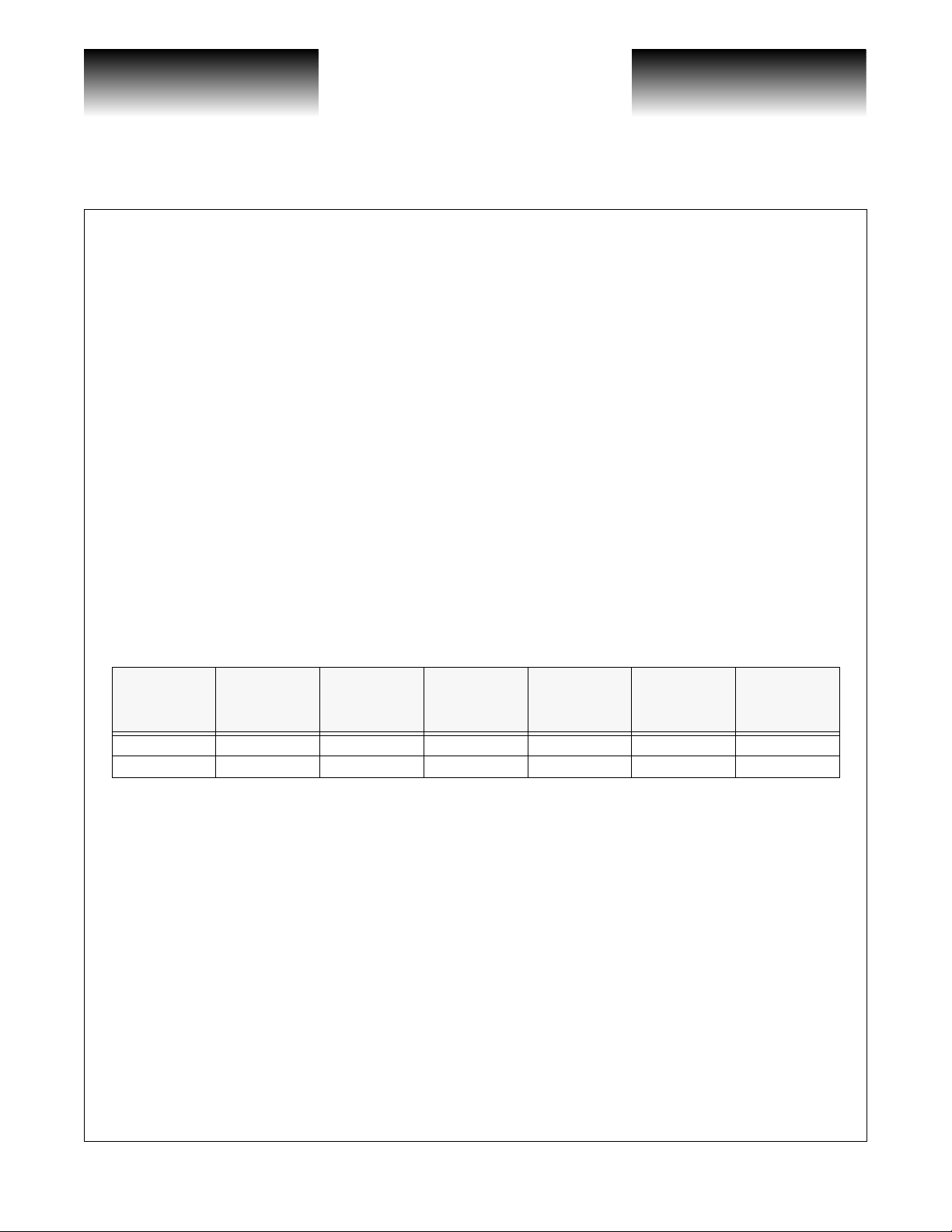
Equipment Loopback
The Equipment Loopback function is controlled by the EQULOOP signal. When the EQULOOP signal is
set high, the Equipment Loopback mode is activated and the high speed transmit data generated from the parallel to serial conversion of the low speed data (TXIN [7:0]) is selected and converted back to parallel data in the
receiver section and presented at the low speed parallel outputs (RXOUT [7:0]). See Figure 4. The internally
generated 155MHz/622MHz clock is used to generate the low speed receive clock output (RXLSCKOUT). In
Equipment Loopback mode the transmit data (TXIN [7:0]) is serialized and presented at the high speed output
(TXDATAOUT).
Page 4
741 Calle Plano, Camarillo, CA 93012 • 805/388-3700 • FAX: 805/987-5896 1/8/00
VITESSE SEMICONDUCTOR CORPORATION
G52220-0, Rev 4.1
VITESSE
SEMICONDUCTOR CORPORATION
Data Sheet
SC8116
ATM/SONET/SDH 622/155Mb/s Transceiver
Mux/Demux with Integrated Clock Generation
Figure 4: Equipment Loopback Data Path
RXDATAIN
RXCLKIN
TXDATAOUT
EQULOOP
DQ
0
1
0
1
Q
D
1:8
Serial to
Parallel
8
÷
8:1
Parallel to
Serial
PLL ÷
D
Q
Q
D
8
RXOUT[7:0]
RXLSCKOUT
TXIN[7:0]
TXLSCKOUT
Split Loopback
Equipment and facili ty loo pbac k modes can be enabled simultaneously. See descript ions f or equipment and
facility loop modes above. The only change is, since they are both active, RXDATAIN will not be deserialized
and presented to RXOUT[0:7], and TXIN[0:7] will not be serialized and present to TXDATAOUT.
Figure 5: Split Loopback Datapath
D
RXDATAIN
RXCLKIN
TXDATAOUT
FACLOOP
DQ
Q
0
1
0
1
D
0
1
0
1
1:8
Serial to
Parallel
÷
8:1
Parallel to
Serial
PLL
8
Q
Q
D
RXOUT[7:0]
RXLSCKOUT
TXIN[7:0]
EQULOOP
Loop Timing
LOOPTIM0 mode bypasses the CMU when the LOOPTIM0 input is asserted high. In this mode the CMU
is bypassed by using the receive clock (RXCLKIN), and the entire part is synchronously clocked from a single
external source.
G52220-0, Rev 4.1
VITESSE SEMICONDUCTOR CORPORATION
1/8/00 741 Calle Plano, Camarillo, CA 93012 • 805/388-3700 • FAX: 805/987-5896
Page 5
VITESSE
SEMICONDUCTOR CORPORATION
ATM/SONET/SDH 622/155Mb/s Transceiver
Mux/Demux with Integrated Clock Generation
Clock Multiplier Unit
The VSC8116 uses an integrated phase-locked loop (PLL) for c lock synthesis of the 622MHz hig h speed
clock used for serialization in the transmitter section. The PLL is comprised of a phase-frequency detector
(PFD), an integrating operation amplifier and a voltage controlled oscillator (VCO) configured in classic feedback system. The PFD compares the selected divided down version of the 622MHz VCO ( CMUFREQSEL
selects divide-by ratios of 8 or 32, see Table 2) and the reference clock. The integrator provides a transfer function between input phase error and output voltage control. The VCO portion of the PLL is a voltage controlled
ring-oscillator with a center frequency of 622MHz.
The reactive elements of the integrator are located off-chip and are connected to the feedback loop of the
amplifier through the CP1, CP2, CN1 and CN2 p ins. The configuration of thes e external surface moun ted
capacitors is shown in Figure 6. Table 1 shows the recommended external capacitor values for the configurable
reference frequencies.
Good analog design practices should be applied to the board design for these external components. Tightly
controlled analog ground and power planes should be provided for the PLL portion of the circuitry. The dedicated PLL power (VDDA) and ground (VSSA) pins should have quiet supply planes to minimize jitter generation within the clock synthesis uni t. This is accomp lished by eithe r using a ferrite be ad or a C-L-C choke (
filter) on the (VDDA) power pins. Note: Vitesse recommends a (π filter) C-L-C choke over using a ferrite bead.
All ground planes should be tied together using multiple vias.
Data Sheet
VSC8116
π
Table 1: Recommended External Capacitor Values
Reference
Frequency
[MHz]
19.44 32 0.1 0.1 X7R 0603/0805 +/-10%
77.76 8 0.1 0.1 X7R 0603/0805 +/-10%
Divide Ratio CP CN Type Size Tol.
Page 6
741 Calle Plano, Camarillo, CA 93012 • 805/388-3700 • FAX: 805/987-5896 1/8/00
VITESSE SEMICONDUCTOR CORPORATION
G52220-0, Rev 4.1
 Loading...