

VITESSE VSC8114QB1, VSC8114QB2, VSC8114QB Datasheet

VITESSE
V
SEMICONDUCTOR CORPORATION
Data Sheet
SC8114
ATM/SONET/SDH 622 Mb/s Transceiver Mux/Demux
with Integrated Clock Generation and Clock Recovery
Features
• Operates at STS-12/STM-4 (622.08Mb/s)
Data Rate
• Compatible with Industry ATM UNI Devices
• On Chip Clock Generation of the 622.08MHz
High Speed Clock (Mux)
• On Chip Clock Recovery of the 622.08MHz
High Speed Clock (Demux)
• 8-Bit Parallel TTL Interface with Parity Error
Detection and Generation
• SONET/SDH Frame Recovery
• Loss of Signal (LOS) Input & LOS Detection
• +3.3V/5V Programmable PECL Serial Interface
• Provides Equipment, Facilities and Split Loopback Modes as well as Loop Timing Mode
• Provide PECL Reference Clock Inputs
• Meets Bellcore, ITU and ANSI Specifications
for Jitter Performance
• Low Power - 0.9Watts Typical
• 100 PQFP Package
General Description
The VSC8114 is an ATM/SONET/SDH compatible transceiver integrating an on-chip Clock Multiplication
Unit (PLL) for high speed clock generation as well as a Clock and data Recovery Unit (CRU) with 8-bit serialto-parallel and parallel-to-serial data conversion. The PLL clock is used for serialization in the transmit direction (Mux). The recovered clock is used for deserialization in the receive direction (Demux). The demultiplexer
contains SONET/SDH frame detection and recovery. In addition, the device provides both facility and equipment loopback modes and a loop time mode. The part is packaged in a 100PQFP with an integrated heat
spreader for optimum thermal performance and reduced cost. The VSC8114 provides an integrated solution for
ATM physical layers and SONET/SDH systems applications.
Functional Description
The VSC8114 is designed to provide a SONET/SDH compliant interface between the high spee d optical
networks and the lower speed User Network Interface devices such as the PM5355 S/UNI-622. The VSC8114
conv ert s 8 bi t pa ra llel d a ta at 7 7.76 Mb/s t o a serial bit stream at 62 2.08 Mb/ s. T he device also provides a Facilit y
Loopback function which loops the received high speed data and clock (optionally recovered on-chip) directly
to the high speed transmit outputs. A Clock Multiplier Unit (CMU) is integrated into the transmit circuit to generate the high speed clock for the serial output data stream from input reference f requencies of 19.44 or 77.76
MHz. The CMU can be bypassed with the received/recovered clock in loop timing mode, thus synchronizing
the entire part to a single clock. The block diagram on page 2 sho ws the maj or function al blocks associ ated with
the VSC8114.
The receive se ction pro vid es the serial-to -parallel co n v ersi on, converting 62 2Mb/s bit st ream to an 8 bi t parallel output at 77.76MHz. A Clock Reco v ery Unit (CRU) is integrated int o th e recei v e ci rcuit to reco ver t he hi gh
speed clock from the recei ved serial data stream. Th e receive section provides an Equipment Loopback funct i on
which will loop the low speed transmit data and clock back through the receive section to the 8 bit parallel out-
puts. The VSC8114 also provides the option of selecting between either its internal CRU’s clock and data signals, or optics containing a CRU clock and data sign al s. The receive section al so co nt ains a SONE T/SDH frame
G52185-0, Rev 4.0
11/1/99 741 Calle Plano, Camarillo, CA 93012 • 805/388-3700 • FAX: 805/987-5896
VITESSE SEMICONDUCTOR CORPORATION
Page 1
VITESSE
4
SEMICONDUCTOR CORPORATION
ATM/SONET/SDH 622 Mb/s Transceiver Mux/Demux
with Integrated Clock Generation and Clock Recovery
Data Sheet
VSC811
detector circuit which is used to provide frame pluses during the A1, A2 boundary in the serial to parallel converter. This only occurs when OOF is high. Both internal and external LOS functions are supported.
The VSC8114 provides the parity error detection and generation for the 8 bit data bus. On the receive side,
the parity of the 8 bit data outputs is generated. On the transmit side, the parity of the 8 bit data input is calculated and compared with the received parity input.
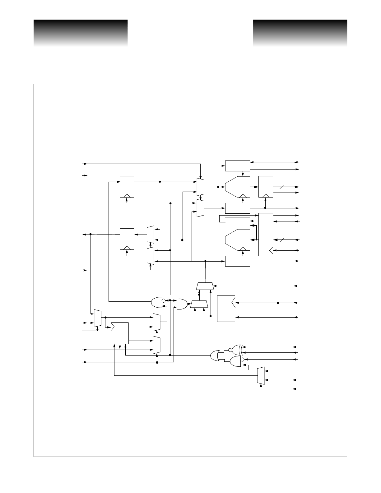
VSC8114 Block Diagram
EQULOOP
RESET
TXDATAOUT+/-
FACLOOP
DQ
DQ
FRAMER
0
1
0
1
1
0
1
0
1:8
DEMUX
Divide-by-8
Parity Chk
8:1
MUX
Divide-by-8
Parity/
REG
REG
8
8
OOF
FP
RXOUT[7:0]
RXOUTP
RXLSCKOUT
TXPERR
TXINP
TXIN[7:0]
TXLSCKIN
TXLSCKOUT
LOOPTIM0
REFCLKP+/-
REFSEL
LOSPECL
LOSTTL
LOSDETEN_
CRUREFCLK
CRUREFSEL
RXDATAIN+/-
CRUEQLP
RXCLKIN+/-
DSBLCRU
01
10
1
0
REC-DATA
CRU
REC-CLK
losdet
1
0
0
1
CMU
0
1
Transmit Section
Byte-wide data is presented to TXIN[7:0] and is clocked into the part on the rising edge of TXLSC KIN.
See Figure 1. The data is th en seria lized (M SB le ading) a nd pr esente d to the TXDATAOUT+/- pins. Th e seria l
output stream is synchronized to the CMU generated clock whic h is a phase locked and frequency scaled ver-
Page 2
741 Calle Plano, Camarillo, CA 93012 • 805/388-3700 • FAX: 805/987-5896 11/1/99
VITESSE SEMICONDUCTOR CORPORATION
G52185-0, Rev 4.0
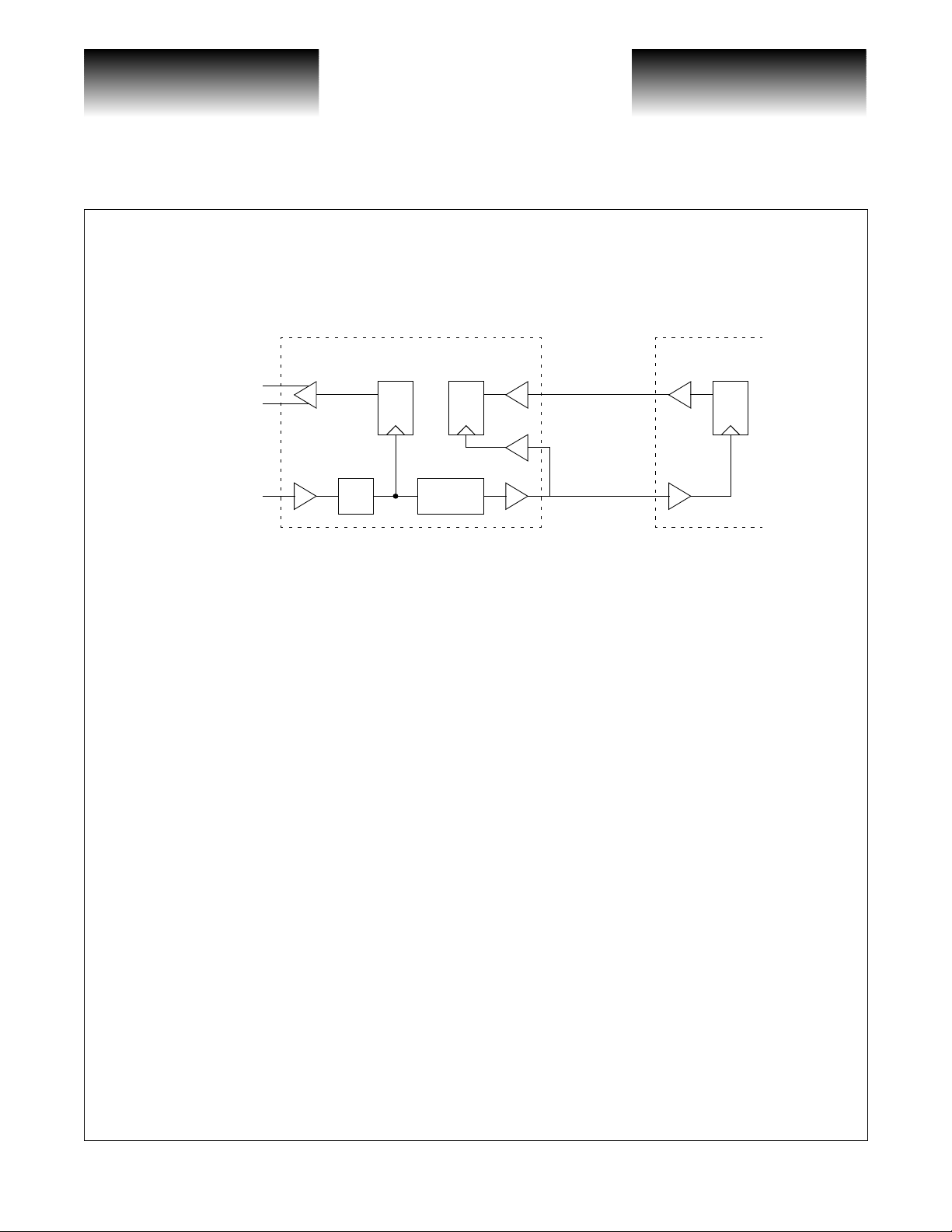
VITESSE
V
SEMICONDUCTOR CORPORATION
Data Sheet
SC8114
sion of the input referen ce clock. Ex ternal control in put REFSEL se lects the mult iply ratio of th e CMU (see
table 11). A divide-by-8 version of the CMU clock (TXLSCKOUT) should be used to synchronize the transmit
interface of the UNI device to the transmit input registers on the VSC8114 (see Application Notes, p. 20).
Figure 1: Data and Clock Transmit Block Diagram
TXDATAOUT+
TXDATAOUT-
REFCLK
Receive Section
High speed Non-Return to Zero (NRZ) serial data at 622M b/s are received by the RXDATAIN inputs. The
CRU recovers the high speed clock from the seria l data i n put. T h e seri al d ata is co nverted to byte-wid e pa rall e l
data and presented on RXOUT[7:0] pins. A divide-by-8 version of the high-speed clock (RXLSCKOUT)
should be used to synchronize the byte-serial RXOUT[7:0] data with the receive portion of the UNI device. The
on-chip CRU is by-passed by setting the DSBLCRU input high. In this mode, the serial input data and corresponding clock are received by the RXDATAIN and RXCLKIN inputs respectively. RXDATAIN is clocked in
on the rising edge of RXCLKIN+. See Figure 2.
The receive section also includes frame detection a nd recovery circuitry which detec ts the SONET/SDH
frame, aligns the received serial data on byte boundaries, and initiates a frame pulse on FP coincident with the
byte aligned data. The frame recovery is initiated when OOF is held high which must occur at lea s t 4 byte clock
cycles before the A1A2 boundary. The OOF input control is a level-sensitive signal, and th e VSC8114 will continually perform frame detection and recovery as long as this pin is held high even if 1 or more frames has been
detected. Frame detection and recovery occurs when a series of three A1 bytes followed by three A2 bytes has
been detected. The paralle l outp ut data on R XOUT[7:0] wil l be b yt e alig ned startin g on the thi rd A2 b yte. Wh en
a frame is detected, a single byte clock pe riod long pulse is g enerated o n FP which i s synchronize d with the
byte-aligned third A2 byte on RXOUT[7:0]. The frame detector sends an FP pulse only if OOF is high.
ATM/SONET/SDH 622 Mb/s Transceiver Mux/Demux
with Integrated Clock Generation and Clock Recovery
VSC8114 PM5355
DQDQ
Divide-by-8CMU
TXIN[7:0]
TXLSCKIN
TXLSCKOUT
DQ
Loss of Signal
The VSC8114 features Loss of Signal (LOS) detection. Loss of Signal is detected if the incoming serial
data stream has no transition continuously for more than 128 bits. During an LOS condition, the VSC 8114
forces the receive data low which is an indication for an y do wnstre am equipment that an optical interfac e fail ure
has occurred. The receive section continues to be clocked by the CRU as it is now locked to the CRUREFCLK
unless DSBLCRU is active, in which case it will be clocked by the CMU. This LOS condition will be removed
when the part detects more than 16 transitions in a 128 bit time window. This LOS detection feature can be disabled by applying a high level to the LOSDETEN_ input. The VSC8114 also has a TTL input LOSTTL and a
G52185-0, Rev 4.0
11/1/99 741 Calle Plano, Camarillo, CA 93012 • 805/388-3700 • FAX: 805/987-5896
VITESSE SEMICONDUCTOR CORPORATION
Page 3
VITESSE
4
SEMICONDUCTOR CORPORATION
ATM/SONET/SDH 622 Mb/s Transceiver Mux/Demux
with Integrated Clock Generation and Clock Recovery
Data Sheet
VSC811
PECL input LOSPECL to force the part into a Loss of Signal stat e. Most optics have a PECL outpu t usually
called “SD” or “FLAG” indicating the presence or lack of optical power. Depending on the optics manufacturer
this signal is either active high or active low. The LOSTTL and LOSPECL inputs are XNOR’d to generate an
internal LOS control signal. See Figure 2. The optics “SD” output should be connect ed to LOSPECL. The
LOSTTL input should be tied to low if the optics “SD” is active high. If it’s active low tie LOSTTL to a high.
The inverse is true if the optics use “FLAG” for loss of signa l
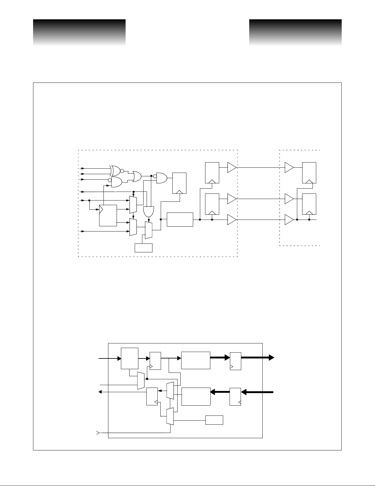
Figure 2: Data and Clock Receive Block Diagram
PM5355
LOSPECL
LOSTTL
LOSDETEN_
DSBLCRU
RXDATAIN+/-
RXCLKIN+/-
Losdet
CRU
1
0
0
1
VSC8114
0
1
DQ
Divide-by-8
DQ
DQ
RXOUT[7:0]
FP
RXLSCKOUT
DQ
DQ
CMU
Facility Loopback
The Facility Loopback function is controlled by the FACLOOP signal. When the FACLOOP signal is set
high, the Facility Loopback mode is activated and the high speed serial receive data (RXDATAIN) is presented
to the high speed transmit output (TXDATAOUT). See Figure 3. In Facility Loopback mode the high speed
receive data (RXDATAIN) is also converted to parallel data and presented to the low speed receive data output
pins (RXOUT[7:0]). The receive clock (RXCLKIN) is also divided down and presented to the low speed clock
output (RXLSCKOUT).
Figure 3: Facility Loopback Data Path
D
RXDATAIN
RXCLKIN
TXDATAOUT
Recovered
Clock
CRU
Q
0
1
Q
1
D
0
1
0
1:8
Serial to
Parallel
8:1
Parallel to
Serial
PLL
D
Q
Q
D
RXOUT[7:0]
TXIN[7:0]
FACLOOP
Page 4
741 Calle Plano, Camarillo, CA 93012 • 805/388-3700 • FAX: 805/987-5896 11/1/99
VITESSE SEMICONDUCTOR CORPORATION
G52185-0, Rev 4.0
VITESSE
V
SEMICONDUCTOR CORPORATION
Data Sheet
SC8114
ATM/SONET/SDH 622 Mb/s Transceiver Mux/Demux
with Integrated Clock Generation and Clock Recovery
Equipment Loopback
The Equipment Loopback function is controlled by the EQULOOP signal. When the EQULOOP signal is
set high, the Equipment Loopback mode is activated and the high speed transmit data generated from the parallel to serial conversion of the low speed data (TXIN[7:0]) is selected and converted back to parallel data in the
receiver section and presented to the low speed parallel o utputs (RXOUT[7:0]). S ee Figure 4. The inte rnally
generated 622MHz clock is used to generate the low speed receive cl ock output (RXLSCKOUT). In Equipment
Loopback mode the transmit data (TXIN[7:0]) is serialized and presented to the high spee d output
(TXDATAOUT) using the clock generated by the on-chip clock multiplier unit.
CRU Equipment Loopback
Exactly the same as equipment loopback, the point where the transmit data is looped back is moved all the
way back to the high speed I/O. When the CRUEQLP signal is set high, transmit data is looped back to the
CRU, replacing RXDATAIN±
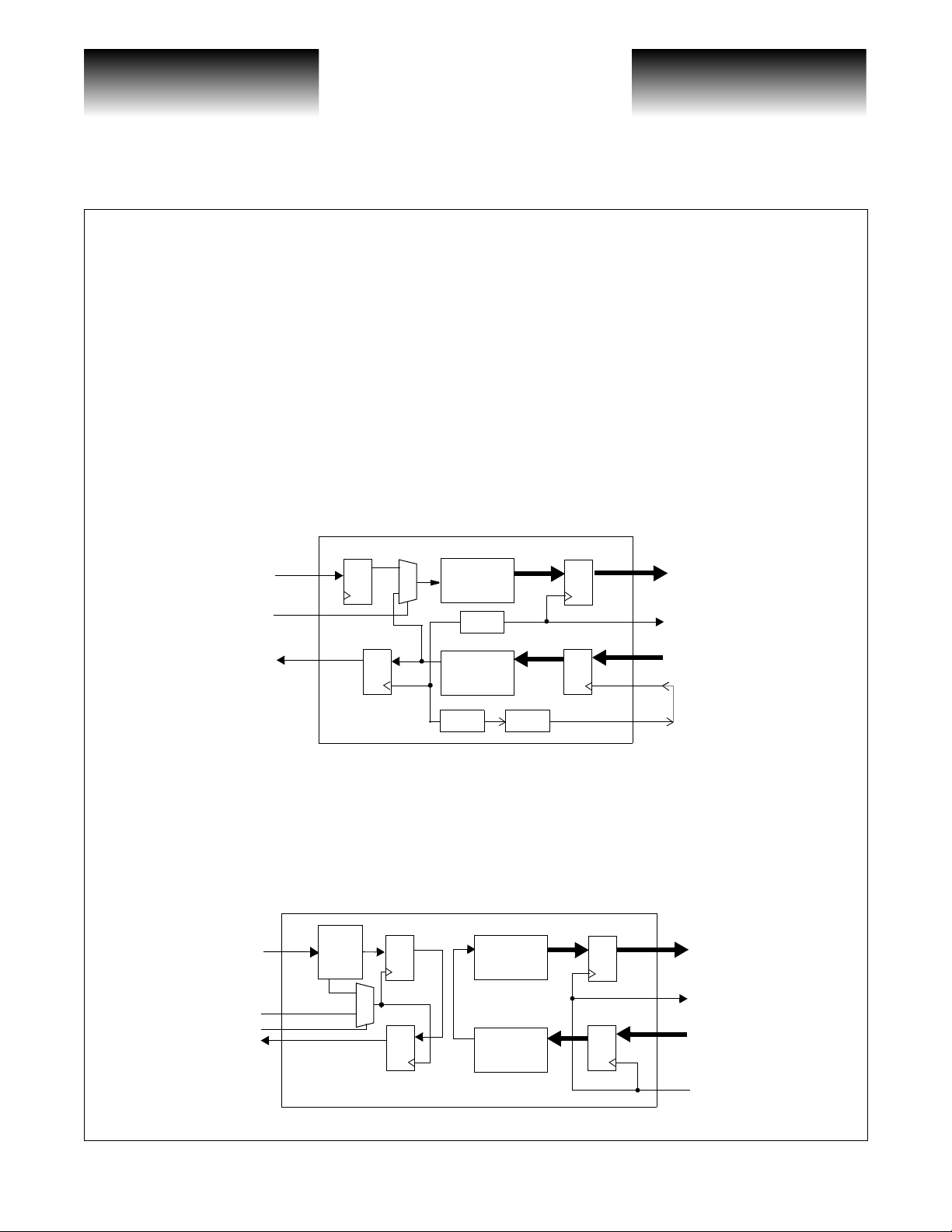
Figure 4: Equipment Loopback Data Path
D
RXDATAIN
EQULOOP
Q
0
1
1:8
Serial to
Parallel
÷
8
D
Q
RXOUT[7:0]
RXLSCKOUT
TXDATAOUT
Q
D
8:1
Parallel to
Serial
PLL ÷
Q
D
8
TXIN[7:0]
TXLSCKIN
TXLSCKOUT
Split Loopback
Equipment and facility loopback modes can be enabled simultaneously. In this case, high-speed serial data
received (RXDATAIN) is mux’d through to the high-speed serial outpu ts (TXD ATA OUT). The lo w-spee d transmit byte-wide bus (TXIN[7:0]) and (TXLSCKIN) is mux’d into the low-speed byte-wide receive output bus
(RXOUT[7:0]) and (RXLSCKOUT). See Figure 5.
Figure 5: Split Loopback Datapath
D
RXDATAIN
RXCLKIN
DSBLCRU
TXDATAOUT
Recovered
Clock
CRU
Q
0
1
Q
D
1:8
Serial to
Parallel
8:1
Parallel to
Serial
D
Q
Q
D
RXOUT[7:0]
RXLSCKOUT
TXIN[[7:0]
TXLSCKIN
G52185-0, Rev 4.0
VITESSE SEMICONDUCTOR CORPORATION
11/1/99 741 Calle Plano, Camarillo, CA 93012 • 805/388-3700 • FAX: 805/987-5896
Page 5

VITESSE
4
SEMICONDUCTOR CORPORATION
ATM/SONET/SDH 622 Mb/s Transceiver Mux/Demux
with Integrated Clock Generation and Clock Recovery
Loop Timing
LOOPTIM0 mode bypasses the CMU when the LOOPTIM0 input is asserted high. In this mode the CMU
is bypassed by using the receive clock (RXCLKIN), and the entire part is synchronously clocked from a single
external source.
Parity
An even parity in put (TXINP) is pr o v id ed fo r the b yt e- wid e transmi t data. Thi s inpu t, along wit h b yt e- wi de
data, is clock ed int o th e VSC 8114 on the r ising edge of TXLSCKIN. P a rit y i s cal cul at ed on t he c lo ck e d in bytewide data and compared to the clocked in parity input. A parity error is reported on the next TXLSCKIN rising
edge on TXPERR. For no parity errors to result, TXINP must be logic 1 when on an odd number of bits in the
TXIN[7:0] are logic 1; otherwise, it must be logic 0.
Even parity is calculated and clocked out along with byte-wide receive data (RXOUT[7:0]) on RXOUTP.
RXOUTP is a logic 1 when an odd number of bits on RXOUT[7:0] are logic 1; ohterwise, it is logic 0.
Clock Synthesis
The VSC8114 uses an integrated phase-locked loop (PLL) for c lock synthesis of the 622MHz hig h speed
clock used for serialization in the transmitter section. The PLL is comprised of a phase-frequency detector
(PFD), an integrating operation amplifier and a voltage controlled oscillator (VCO) configured in classic feedback system. The PFD compares the selected divided down version of the 622MHz VCO (select pin REFSEL
selects divide-by ratios of 8 and 32, see Table 11) and the reference clock. The integrator provides a transfer
function between input phase error and ou tput voltage control. The V CO portion of the PLL is a voltage controlled ring-oscillator with a center frequency of 622MHz.
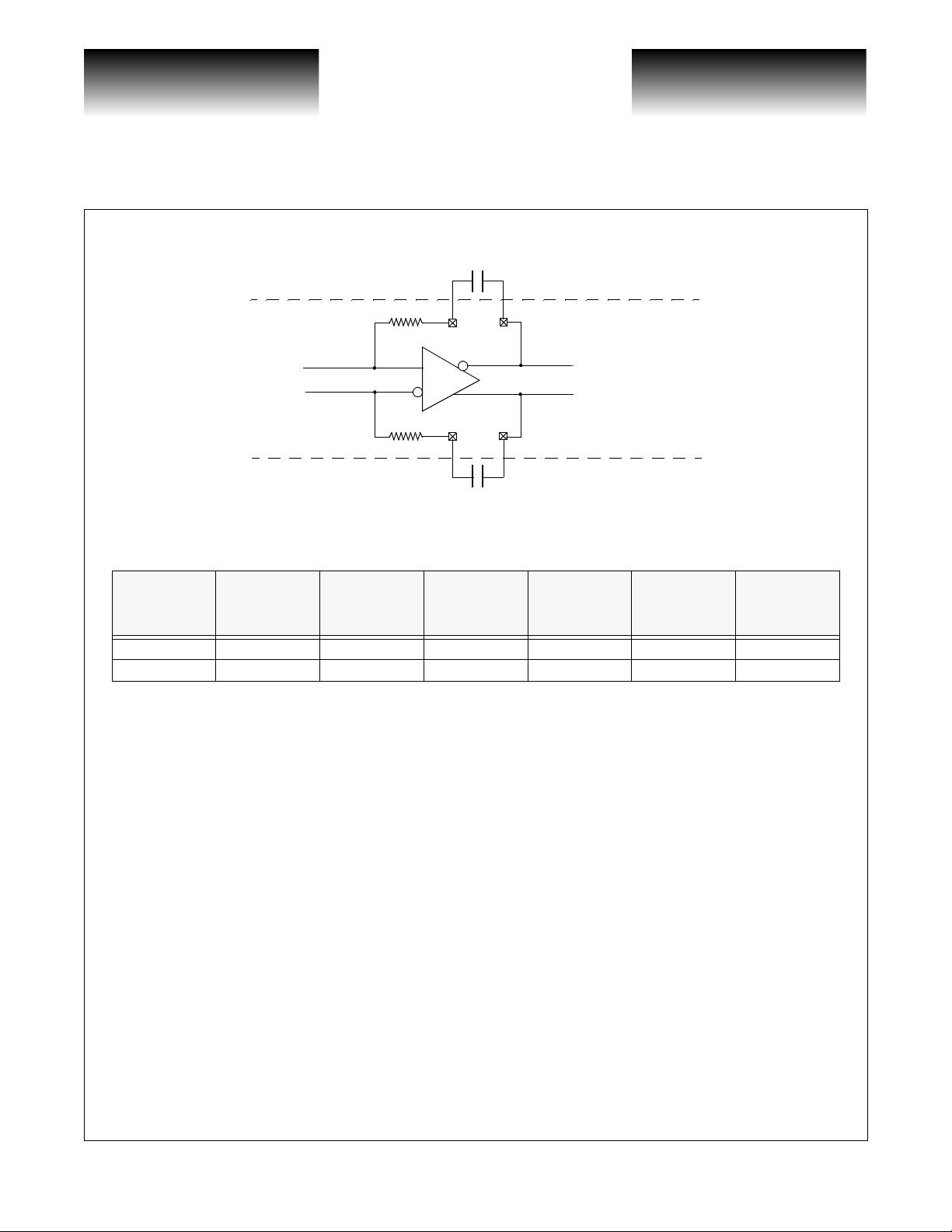
The reactive elements of the integrator are located off-chip and are connected to the feedback loop of the
amplifier through the CP1, CP2, CN1 and CN2 p ins. The configuration of thes e external surface moun ted
capacitors is shown in Figure 6. Table 1 shows the recommended external capacitor values for the configurable
reference frequencies.
Good analog design practices should be applied to the board design for these external components. Tightly
controlled analog ground and power planes should be provided for the PLL portion of the circuitry. The dedicated PLL power (VDDANA) and ground (VSSANA) pins should have quiet supply planes to minimize jitter
generation within the clock synthesis unit. This is accomplished by either using a ferrite bead or a C-L-C choke
(π filter) on the (VDDANA) power pins. Note: Vitesse recommends a (π filter) C-L-C choke over using a ferrite
bead. All ground planes should be tied together using multiple vias.
Data Sheet
VSC811
Reference Clocks
Note that the CMU uses a differential PECL reference clock input to achieve optimum jitter performance.
The CRU has the option of either using the CMU’s reference clock or its own independent reference clock
CRUREFCLK. This is accomplished with the control signal CRUREFSEL. The CRUREFCLK should be used
if the system is being operate d in ei t her a r e ge ner at io n or loo p ti mi ng mode . In either of t hese modes the qu ali t y
of the CR UREFCLK is not a concer n, t hus it can be dr i v en b y a si mple 7 7.76MHz cryst al, t he k ey is it s inde pendence from the CMU’s reference clock.
Page 6
741 Calle Plano, Camarillo, CA 93012 • 805/388-3700 • FAX: 805/987-5896 11/1/99
VITESSE SEMICONDUCTOR CORPORATION
G52185-0, Rev 4.0
VITESSE
V
SEMICONDUCTOR CORPORATION
Data Sheet
SC8114
Figure 6: External Integrator Capacitor
Table 1: Recommended External Capacitor Values
Reference
Frequency
[MHz]
19.44 32 0.1 0.1 X7R 0603/0803 +/-10%
77.76 8 0.1 0.1 X7R 0603/0803 +/-10%
Divide Ratio CP CN Type Size Tol.
ATM/SONET/SDH 622 Mb/s Transceiver Mux/Demux
with Integrated Clock Generation and Clock Recovery
CP = 0.1 µF
CP1
+
-
CN1 CN2
CP2
CN = 0.1 µF
Clock Recovery
The fully monolithic Clock Recovery Unit (CRU) consists of a Phase Detector, a Frequency Detector, a
Loop Filter and a Voltage Controlled Oscillator (VCO). The phase detector compares the phase information of
the incoming data with the recovered clock. The frequency detector compares the frequency component of the
data input with the recovered clock to provide the pull in energy during lock acquisition. The Loop Filter integrates the phase information from the phase and frequency detectors and provides the control voltage to the
VCO.
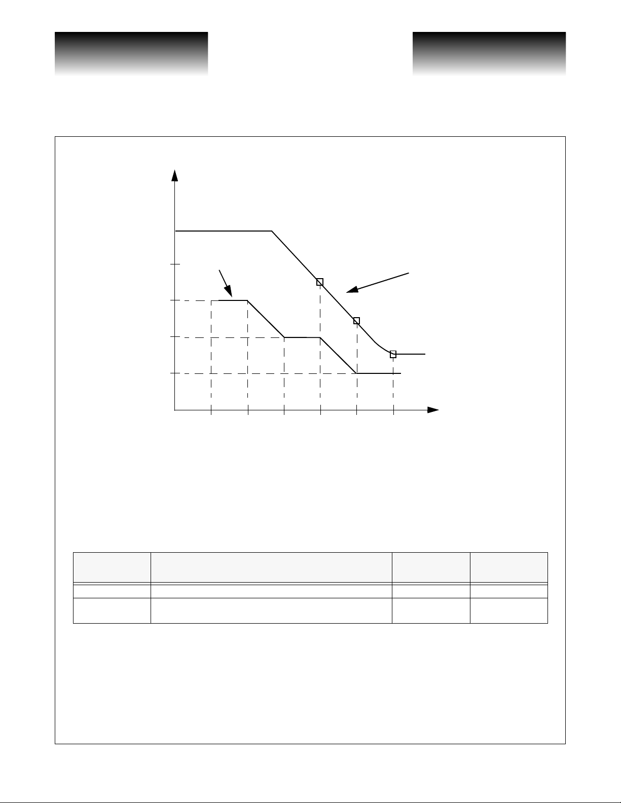
Jitter Tolerance
Jitter Tolerance is the ability of the Clock Recovery Unit to track timing variations in the received data
stream. The Bellcore and ITU specifications allow the received optical data to co ntain jitter. The amount that
must be tolerated is a fun ction of the fr equ ency of the jitter. The CRU is designed to to lerat e jitter with ma rgin
over the specification limits, see F igure 7. T he CRU obtains and main tains lock based on the data transi tion
information. When there is no transition on the data stream, the recovered clock frequency can drift. The
VSC8114 can maintain lock over 100 bits of no switching on the data stream.
G52185-0, Rev 4.0
11/1/99 741 Calle Plano, Camarillo, CA 93012 • 805/388-3700 • FAX: 805/987-5896
VITESSE SEMICONDUCTOR CORPORATION
Page 7
VITESSE
4
SEMICONDUCTOR CORPORATION
ATM/SONET/SDH 622 Mb/s Transceiver Mux/Demux
with Integrated Clock Generation and Clock Recovery
Figure 7: Jitter Tolerance
JITTER(UI P-P)
150
15
1.5
0.15
Bellcore Requirement
60
Data Sheet
VSC811
VSC8114 Guaranteed
Jitter Tolerance
6
0.6
10 30 300 25K 250K
Data Latency
The VSC8114 contains several operating modes, each of which exercise different logic paths through the
part. Table 2 bounds the data latency through each path with an associated clock signal.
Table 2: Data Latency
Circuit Mode Description
Receive MSB at RXDATAIN to data on RXOUT [7:0] RXCLKIN 25-35
Facilities
Loopback
MSB at RXDATAIN to MSB at TXDATAOUT RXCLKIN 2-4
2.5M
JITTER FREQ(HZ)
Clock
Reference
Range of Clock
cycles
Page 8
741 Calle Plano, Camarillo, CA 93012 • 805/388-3700 • FAX: 805/987-5896 11/1/99
VITESSE SEMICONDUCTOR CORPORATION
G52185-0, Rev 4.0
 Loading...