

VITESSE VSC8111QB2, VSC8111QB1, VSC8111QB Datasheet
G52142-0, Rev 4.2
VITESSE
SEMICONDUCTOR CORPORATION
Page 1
8/31/98 741 Calle Plano, Camarillo, CA 93012 • 805/388-3700 • FAX: 805/987-5896
VITESSE
SEMICONDUCTOR CORPORATION
Data Sheet
SC8111
ATM/SONET/SDH 155/622 Mb/s Transceiver
Mux/Demux with Integrated Clock Generation
Features
General Description
The VSC8111 is an ATM/SONET/SDH compatible transceiver integrating an on-chip clock multiplication
unit (PLL) for the high speed clock and 8 bit serial-to-parallel and parallel-to-serial data conversion. The high
speed clock generated by the on-chip PLL is selectable for 155.52 or 622.08 MHz operation. The demultiplexer
contains SONET/SDH frame detection and recovery. In addition, the device provides both facility and equipment loopback modes and two loop timing modes. The part is packaged in a 100 PQFP with an integrated heat
spreader for optimum thermal performance and reduced cost. The VSC8111 provides an integrated solution for
ATM physical layers and SONET/SDH systems applications.
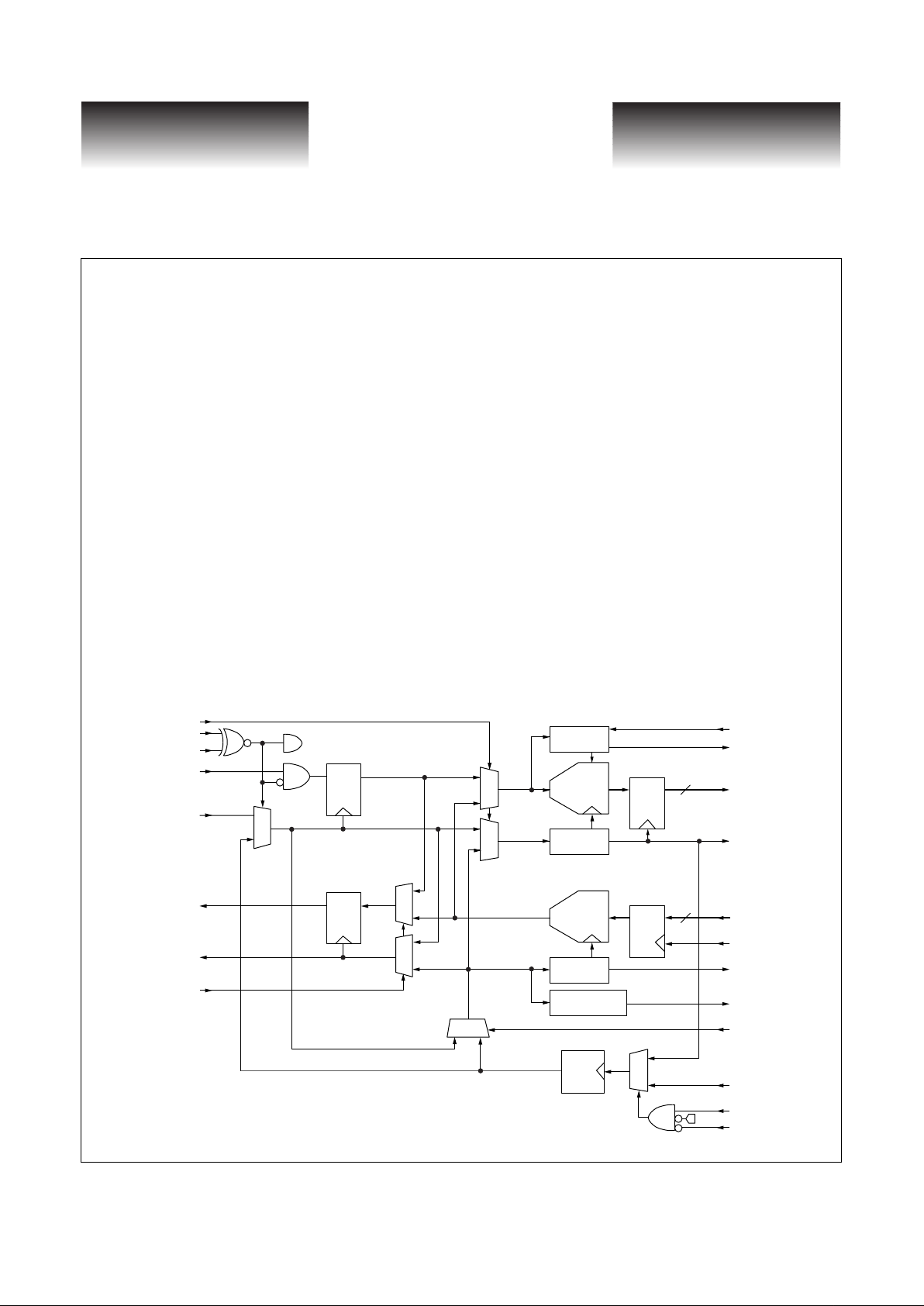
VSC8111 Block Diagram
• Loss of Signal (LOS) Control
• Provides Equipment, Facilities and Split Loopback Modes as well as Loop Timing Mode
• Meets Bellcore, ITU and ANSI Specifications for
Jitter Performance
• Single 3.3V Supply Voltage
• Low Power - 1.4 Watts Maximum
• 100 PQFP Package
• Operates at Either STS-3/STM-1 (155.52 Mb/s) or
STS-12/STM-4 (622.08 Mb/s) Data Rates
• Compatible with Industry ATM UNI Devices
• On Chip Clock Generation of the 155.52 Mhz
or 622.08 Mhz High Speed Clock
• Dual 8 Bit Parallel TTL Interface
• SONET/SDH Frame Detection and Recovery
DQ
0
1
LOSTTL
LOS (Internal Signal)
LOSPOL
RXDATAIN+/-
RXCLKIN+/-
0
1
0
1
DQ
0
1
0
1
8
RXOUT[7:0]
RXLSCKOUT
FP
OOF
EQULOOP
TXDATAOUT+/-
TXCLKOUT+/-
8
TXIN[7:0]
TXLSCKOUT
TXLSCKIN
0
1
FACLOOP
LOOPTIM0
REFCLK
LOOPTIM1
CMU
Divide-by-8
1:8
DEMUX
FRAMER
Divide-by-8
8:1
MUX
01
DQ
QD
Divide-by-3/12 RX50MCK
LOS
EQULOOP
VITESSE
SEMICONDUCTOR CORPORATION
Data Sheet
VSC8111
ATM/SONET/SDH 155/622 Mb/s Transceiver
Mux/Demux with Integrated Clock Generation
Page 2
VITESSE
SEMICONDUCTOR CORPORATION
G52142-0, Rev 4.2
741 Calle Plano, Camarillo, CA 93012 • 805/388-3700 • FAX: 805/987-5896 8/31/98
Functional Description
The VSC8111 is designed to provide a SONET/SDH compliant interface between the high speed optical
networks and the lower speed User Network Interface (UNI) devices such as the PM5355 S/UNI-622 (or
PM5312 STTX). The VSC8111 transmit section converts 8 bit parallel data at 77.76 Mb/s or 19.44 Mb/s to a
serial bit stream at 622.08 Mb/s or 155.52 Mb/s, respectively. It also provides a Facility Loopback function
which loops the received high speed data and clock directly to the transmit outputs. A Clock Multiplier Unit
(CMU) is integrated into the transmit circuit to generate the high speed clock for the serial output data stream
from input references frequency of 19.44, 38.88, 51.84 or 77.76 MHz. The CMU can be bypassed by using the
receive clock in loop timing mode thus synchronizing the entire part to a single clock (RXCLKIN).
The receive section provides the serial-to-parallel conversion, converting 155 Mb/s or 622 Mb/s to an 8 bit
parallel output at 19.44 Mb/s or 77.76 Mb/s, respectively. The receive section provides an Equipment Loopback
function which will loop the low speed transmit data and clock back through the receive section to the 8 bit parallel data bus and clock outputs. The receive section also contains a SONET/SDH frame detector circuit which
is used to provide frame recovery in the serial to parallel converter. The block diagram on page 1 shows the
major functional blocks associated with the VSC8111.
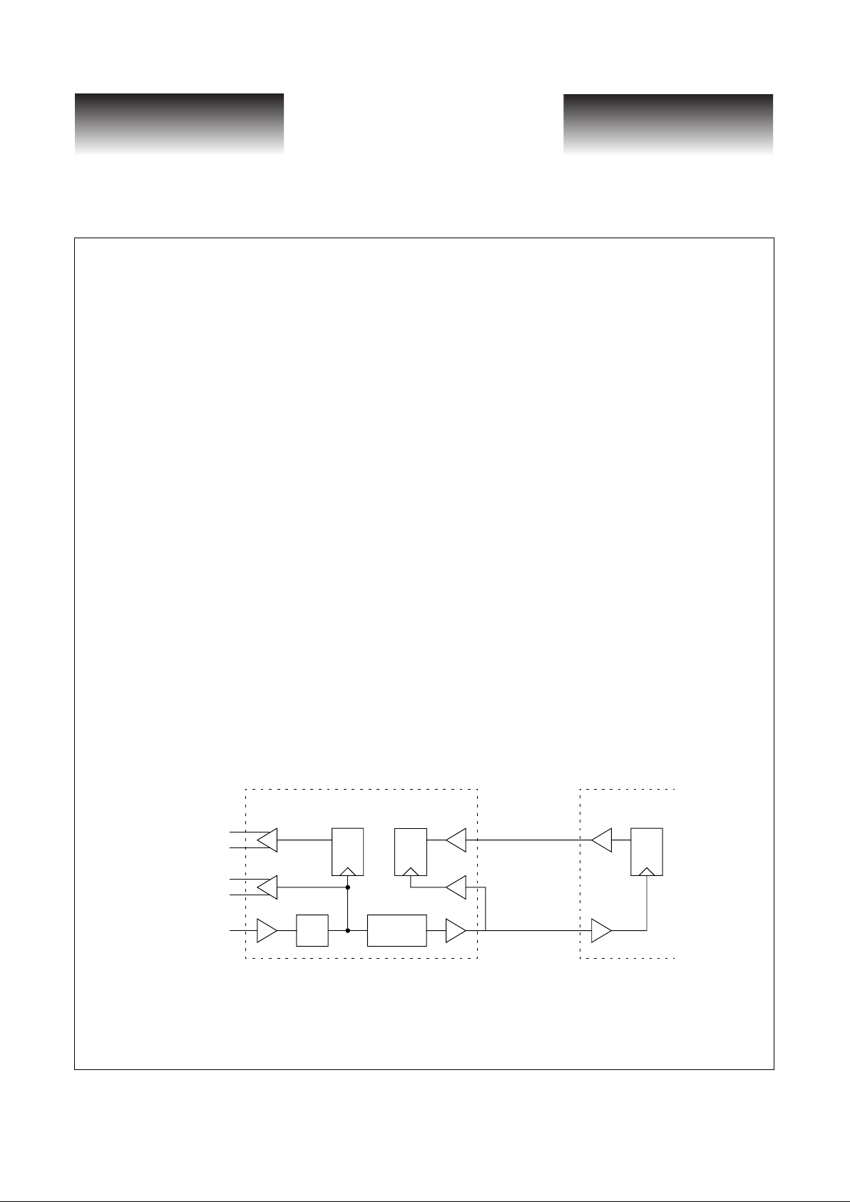
Transmit Section
Byte-wide data is presented to TXIN [7:0] and is clocked into the part on the rising edge of TXLSCKIN
(refer to Figure 1). The data is then serialized (MSB leading) and presented at the TXDATAOUT+/- pins.
TXDATAOUT is clocked out on the falling edge of TXCLKOUT+. The serial output stream is synchronized to
the CMU generated clock which is a phase locked and frequency scaled version of the input reference clock.
External control inputs B0-B2 and STS12 select the multiply ratio of the CMU and either STS-3 (155 Mb/s) or
STS-12 (622 Mb/s) transmission (See Table 2). A divide-by-8 version of the CMU clock (TXLSCKOUT)
should be used to synchronize the transmit interface of the UNI device to the transmit input registers on the
VSC8111. (See Application Notes, Pg. 22)
Figure 1: Data and Clock Transmit Block Diagram
DQDQ
Divide-by-8CMU
DQ
TXIN[7:0]
TXLSCKIN
TXLSCKOUT
TXDATAOUT+
TXDATAOUT-
TXCLKOUT+
TXCLKOUT-
REFCLK
VSC8111 PM5355
G52142-0, Rev 4.2
VITESSE
SEMICONDUCTOR CORPORATION
Page 3
8/31/98 741 Calle Plano, Camarillo, CA 93012 • 805/388-3700 • FAX: 805/987-5896
VITESSE
SEMICONDUCTOR CORPORATION
Data Sheet
SC8111
ATM/SONET/SDH 155/622 Mb/s Transceiver
Mux/Demux with Integrated Clock Generation
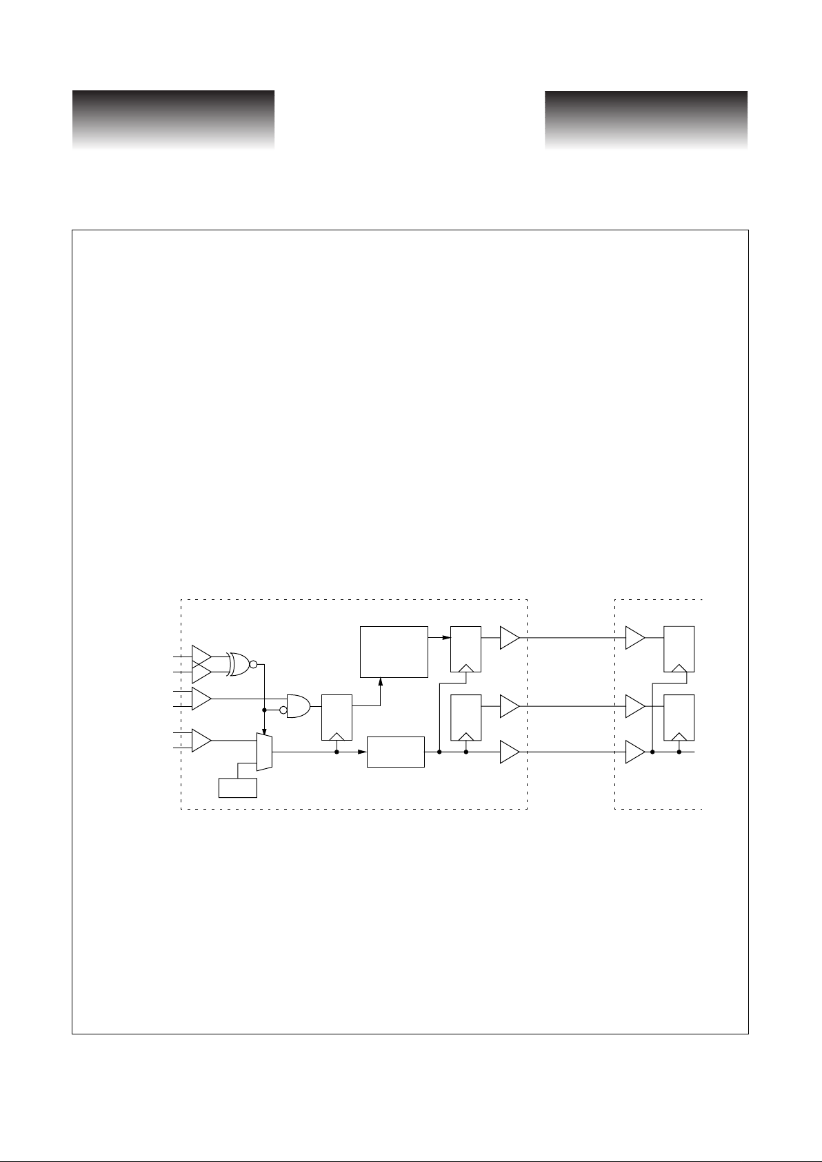
Receive Section
High speed Non-Return to Zero (NRZ) serial data at 155Mb/s or 622Mb/s are received by the RXDATAIN
inputs. RXDATAIN is clocked in on the rising edge of RXCLKIN+. See Figure 2. The serial data is converted to
byte-wide parallel data and presented on RXOUT[7:0] pins. A divide-by-8 version of the high-speed clock
(RXLSCKOUT) should be used to synchronize the byte-serial RXOUT[7:0] data with the receiv e portion of the
UNI device.
The receive section also includes frame detection and recovery circuitry which detects the SONET/SDH
frame, aligns the received serial data on byte boundaries, and initiates a frame pulse on FP coincident with the
byte aligned data. The frame recovery is initiated when OOF is held high which must occur at least 4 byte clock
cycles before the A1A2 boundary. The OOF input control is a level-sensiti ve signal, and the VSC8111 will continually perform frame detection and recovery as long as this pin is held high even if 1 or more frames has been
detected. Frame detection and recovery occurs when a series of three A1 bytes followed by three A2 bytes has
been detected. The parallel output data on RXOUT[7:0] will be byte aligned starting on the third A2 byte. When
a frame is detected, a single byte clock period long pulse is generated on FP which is synchronized with the
byte-aligned third A2 byte on RXOUT[7:0]. The frame detector sends an FP pulse only if OOF is high or if a
frame was detected while OOF was being pulled low.
Figure 2: Data and Clock Receive Block Diagram
Loss of Signal
During a LOS condition, the VSC8111 forces the receive data low which is an indication for any downstream
equipment that an optical interface failure has occurred. The receiv e section is clock ed by the transmit section’s
DQ
DQDQ
0
1
Divide-by-8
CMU
DQ
PM5355
DQ
RXOUT[7:0]
FP
RXLSCKOUT
VSC8111
RXDATAIN+
RXDATAIN-
RXCLKIN+
RXCLKIN-
LOSPOL
LOSTTL
1:8 Serial
to Parallel
VITESSE
SEMICONDUCTOR CORPORATION
Data Sheet
VSC8111
ATM/SONET/SDH 155/622 Mb/s Transceiver
Mux/Demux with Integrated Clock Generation
Page 4
VITESSE
SEMICONDUCTOR CORPORATION
G52142-0, Rev 4.2
741 Calle Plano, Camarillo, CA 93012 • 805/388-3700 • FAX: 805/987-5896 8/31/98
PLL clock multiplier. The VSC8111 has two TTL inputs LOSTTL and LOSPOL one to force the part into a
Loss of Signal state, the other to control the polarity. The LOSTTL and LOSPOL inputs are XNOR’d to generate an internal LOS control signal. See Figure 2. Optics have either a PECL or TTL output, usually called “SD”
(Signal Detect) or “FLAG” indicating either a lack of or presence of optical power. Depending on the optics
manufactured this signal is either active high or active low polarity. If the optics Signal Detect or FLAG output
is a “TTL” signal it should be connected to LOSTTL. If it’s a “PECL” signal it should be connected through a
“PECL” to “TTL” translator (such as the Motorola “MC100ELT21”) which then drives LOSPOL. The
LOSTTL input should be tied low if the optics “SD” or FLAG output is active high. If it’s active low tie
LOSTTL high. Note: LOSPOL and LOSTTL are interchangeable. The follow on part to VSC8111 is the
VSC8113, in this device the signal LOSPOL has been changed to LOSPECL a PECL input, which is why
LOSTTL is being used as the polarity control input.
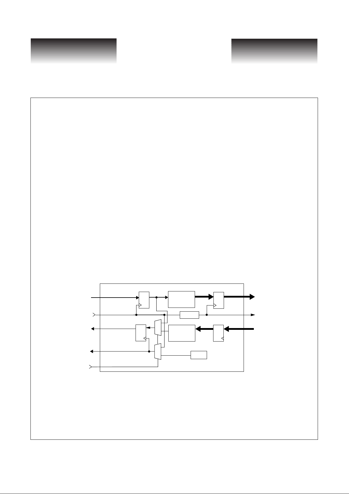
Facility Loopback
The Facility Loopback function is controlled by the FACLOOP signal. When the FACLOOP signal is set
high, the Facility Loopback mode is activated and the high speed serial receive data (RXDATAIN) is presented
at the high speed transmit output (TXDATAOUT). See Figure 3. In addition, the high speed receive clock input
(RXCLKIN) is selected and presented at the high speed transmit clock output (TXCLKOUT). In Facility Loopback mode the high speed receive data (RXDATAIN) is also converted to parallel data and presented at the low
speed receive data output pins (RXOUT [7:0]). The receive clock (RXCLKIN) is also divided down and presented at the low speed clock output (RXLSCKOUT).
Figure 3: Facility Loopback Data Path
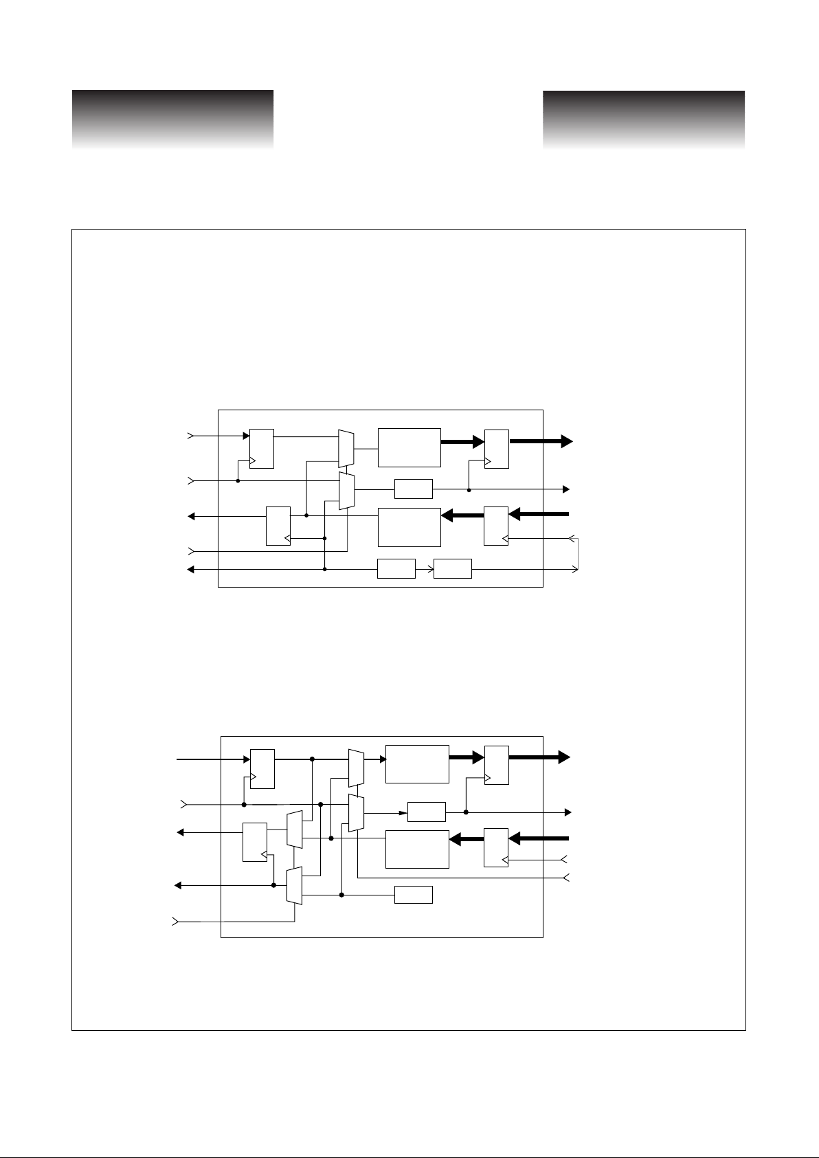
Equipment Loopback
The Equipment Loopback function is controlled by the EQULOOP signal. When the EQULOOP signal is
set high, the Equipment Loopback mode is activated and the high speed transmit data generated from the paral-
D
Q
D
Q
1:8
Serial to
Parallel
Q
D
RXDATAIN
TXDATAOUT
RXOUT[7:0]
Q
D
TXIN[7:0]
8:1
Parallel to
Serial
PLL
0
1
TXCLKOUT
FACLOOP
RXCLKIN
0
1
RXLSCKOUT
÷8
G52142-0, Rev 4.2
VITESSE
SEMICONDUCTOR CORPORATION
Page 5
8/31/98 741 Calle Plano, Camarillo, CA 93012 • 805/388-3700 • FAX: 805/987-5896
VITESSE
SEMICONDUCTOR CORPORATION
Data Sheet
SC8111
ATM/SONET/SDH 155/622 Mb/s Transceiver
Mux/Demux with Integrated Clock Generation
lel to serial conversion of the low speed data (TXIN [7:0]) is selected and converted back to parallel data in the
receiver section and presented at the low speed parallel outputs (RXOUT [7:0]). See Figure 4. The internally
generated 155MHz/622MHz clock is used to generate the low speed receive clock output (RXLSCKOUT). In
Equipment Loopback mode the transmit data (TXIN [7:0]) is serialized and presented at the high speed output
(TXDATAOUT) along with the high speed transmit clock (TXCLKOUT) which is generated by the on board
clock multiplier unit.
Figure 4: Equipment Loopback Data Path
Split Loopback
Equipment and facility loopback modes can be enabled simultaneously . See descriptions for equipment and
facility loop modes above. The only change is, since they are both active, RXDATAIN will not be deserialized
and presented to RXOUT[0:7] and TXIN[0:7] will not be serialized and present to TXDATAOUT.
Figure 5: Split Loopback Datapath
DQ
D
Q
1:8
Serial to
Parallel
Q
D
RXDATAIN
TXDATAOUT
RXOUT[7:0]
Q
D
8:1
Parallel to
Serial
TXIN[7:0]
÷ 8
PLL ÷ 8
RXLSCKOUT
TXLSCKIN
TXLSCKOUT
TXCLKOUT
0
1
EQULOOP
0
1
RXCLKIN
D
Q
1:8
Serial to
Parallel
RXOUT[7:0]
Q
D
8:1
Parallel to
Serial
TXIN[[7:0]
RXLSCKOUT
DQ
Q
D
RXDATAIN
TXDATAOUT
0
1
TXCLKOUT
FACLOOP
RXCLKIN
0
1
÷ 8
PLL
TXLSCLKIN
0
1
EQULOOP
0
1
VITESSE
SEMICONDUCTOR CORPORATION
Data Sheet
VSC8111
ATM/SONET/SDH 155/622 Mb/s Transceiver
Mux/Demux with Integrated Clock Generation
Page 6
VITESSE
SEMICONDUCTOR CORPORATION
G52142-0, Rev 4.2
741 Calle Plano, Camarillo, CA 93012 • 805/388-3700 • FAX: 805/987-5896 8/31/98
Loop Timing
LOOPTIM0 mode bypasses the CMU when the LOOPTIM0 input is asserted high. In this mode the CMU
is bypassed by using the receive clock (RXCLKIN), and the entire part is synchronously clocked from a single
external source.
LOOPTIM1 mode bypasses the REFCLK input and uses the divide-by-8 version of the receive clock as the
reference input to the CMU. This mode is selected by asserting the LOOPTIM1 input high. The part is forced
out of this mode if it is in the Loss of Signal state or in Equipment Loopback to prevent the CMU from feeding
its own clock back. The user needs to set the B[0:2] inputs to select 78MHz operation to match the RXLSCKOUT frequency.
Clock Multiplier Unit
The VSC8111 uses an integrated phase-locked loop (PLL) for clock synthesis of the 622MHz high speed
clock used for serialization in the transmitter section. The PLL is comprised of a phase-frequency detector
(PFD), an integrating operation amplifier and a voltage controlled oscillator (VCO) configured in classic feedback system. The PFD compares the selected divided down version of the 622MHz VCO (select pins B0-B2
select divide-by ratios of 8, 12, 16 and 32, see Table 2) and the reference clock. The integrator provides a transfer function between input phase error and output voltage control. The VCO portion of the PLL is a v oltage controlled ring-oscillator with a center frequency of 622MHz.
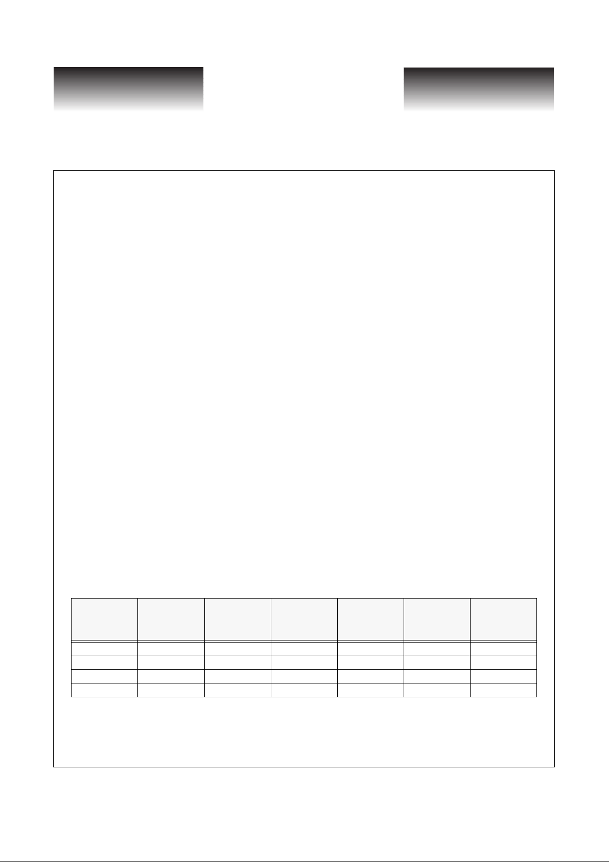
The reactive elements of the integrator are located off-chip and are connected to the feedback loop of the
amplifier through the CP1, CP2, CN1 and CN2 pins. The configuration of these external surface mounted
capacitors is shown in Figure 6. Table 1 shows the recommended external capacitor values for the configurable
reference frequencies.
Good analog design practices should be applied to the board design for these external components. Tightly
controlled analog ground and power planes should be provided for the PLL portion of the circuitry. The dedicated PLL power (VDDANA) and ground (VSSANA) pins should have quiet supply planes to minimize jitter
generation within the clock synthesis unit. This is accomplished by either using a ferrite bead or a C-L-C choke
(
π
filter) on the (VDDANA) power pins. Note: V itesse recommends a ( π filter) C-L-C choke over using a ferrite
bead. All ground planes should be tied together using multiple vias.
Table 1: Recommended External Capacitor Values
Reference
Frequency
[MHz]
Divide Ratio CP CN Type Size Tol.
19.44 32 0.1 0.1 X7R 0603/0803 +/-10%
38.88 16 0.1 0.1 X7R 0603/0803 +/-10%
51.84 12 0.1 0.1 X7R 0603/0803 +/-10%
77.76 8 0.1 0.1 X7R 0603/0803 +/-10%
G52142-0, Rev 4.2
VITESSE
SEMICONDUCTOR CORPORATION
Page 7
8/31/98 741 Calle Plano, Camarillo, CA 93012 • 805/388-3700 • FAX: 805/987-5896
VITESSE
SEMICONDUCTOR CORPORATION
Data Sheet
SC8111
ATM/SONET/SDH 155/622 Mb/s Transceiver
Mux/Demux with Integrated Clock Generation
Figure 6: External Integrator Capacitor
Clock Multiplier Unit
Table 2: Reference Frequency Selection and Output Frequency Control
STS12
B2 B1 B0
Reference
Frequency
[MHz]
Output
Frequency
[MHz]
111019.44 622.08
101038.88 622.08
100151.84 622.08
100077.76 622.08
011019.44 155.52
001038.88 155.52
000151.84 155.52
000077.76 155.52
+
-
CP1
CP2
CN1 CN2
CP = 0.1µF
CN = 0.1µF
VITESSE
SEMICONDUCTOR CORPORATION
Data Sheet
VSC8111
ATM/SONET/SDH 155/622 Mb/s Transceiver
Mux/Demux with Integrated Clock Generation
Page 8
VITESSE
SEMICONDUCTOR CORPORATION
G52142-0, Rev 4.2
741 Calle Plano, Camarillo, CA 93012 • 805/388-3700 • FAX: 805/987-5896 8/31/98
Table 3: Clock Multiplier Unit Performance
(1) These Reference Clock Jitter limits are required for the outputs to meet SONET system level jitter requirements
(< 10 mUIrms)
(2) Needed to meet SONET output frequency stability requirements
(3) Measured
Note: Jitter specification is defined utilizing a 12KHz - 5MHz LP-HP single pole filter.
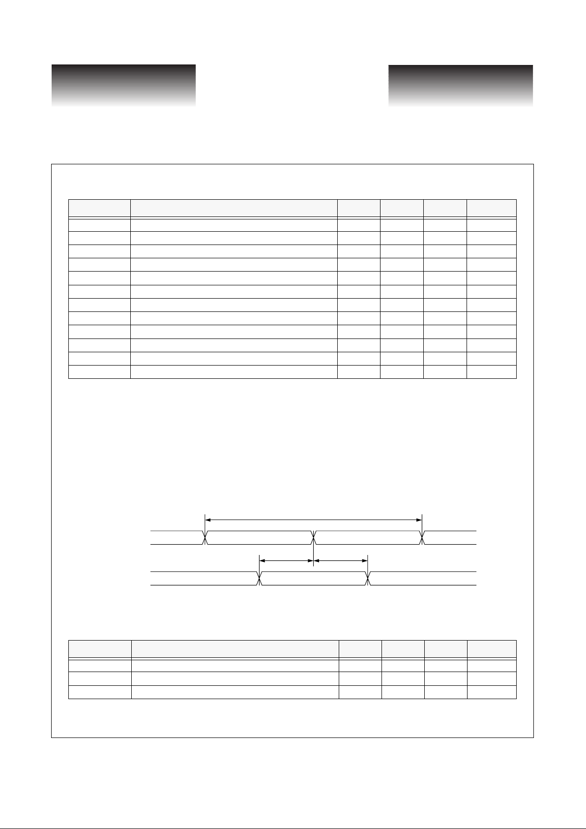
AC Timing Characteristics
Figure 7: Receive High Speed Data Input Timing Diagram
Table 4: Receive High Speed Data Input Timing Table
(STS-12 Operation)
Name Description Min Typ Max Units
RCd Reference clock duty cycle 40 60 %
RCj Reference clock jitter (RMS) @ 77.76 MHz ref
(1)
13 ps
RCj Reference clock jitter (RMS) @ 51.84 MHz ref
(1)
12 ps
RCj Reference clock jitter (RMS) @ 38.88 MHz ref
(1)
9ps
RCj Reference clock jitter (RMS) @ 19.44 MHz ref
(1)
5ps
RC
f
Reference clock frequency tolerance
(2)
-20 +20 ppm
OCj Output clock jitter (RMS) @ 77.76 MHz ref
(3)
8ps
OCj Output clock jitter (RMS) @ 51.84 MHz ref
(3)
10 ps
OCj Output clock jitter (RMS) @ 38.88 MHz ref
(3)
13 ps
OCj Output clock jitter (RMS) @ 19.44 MHz ref
(3)
15 ps
OCfrange Output frequency 620 624 MHz
OCd Output clock duty cycle 40 60 %
Parameter Description Min Typ Max Units
T
RXCLK
Receive clock period - 1.608 - ns
T
RXSU
Serial data setup time with respect to RXCLKIN 250 - - ps
T
RXH
Serial data hold time with respect to RXCLKIN 250 - - ps
T
RXCLK
T
RXSU
T
RXH
RXCLKIN+
RXCLKIN-
RXDATAIN+
RXDATAIN-
 Loading...