

VITESSE VSC8110GB2, VSC8110GB, VSC8110GB1 Datasheet

®
VITESSE Semiconductor Corporation
Page 1
VSC8110
Data Sheet
ATM/SONET/SDH 155/622 Mb/s Transceiv
er
Mux/Demux with Integrated Clock Generation
G51011-0, Rev. 1.5
VITESSE
Features
General Description
The VSC8110 is an ATM/SONET/SDH compatible transceiver integrating high speed clock generation
with 8 bit serial-to-parallel and parallel-to-serial data conversion. The high speed clock is generated using an
on-chip PLL which is selectable for 155.52 or 622.08 Mhz operation. The part can be used with 19.44, 38.88,
51.84 or 77.76 Mhz external reference clocks. The demultiplexer contains SONET/SDH frame detection and
recovery. In addition, the device provides both facility and equipment loopback modes. The part is packaged in
a 100PQFP with integrated heat spreader for optimum thermal performance and reduced cost. The VSC8110
provides an integrated solution for ATM physical layers and SONET/SDH systems applications.
Functional Description
The VSC8110 is designed to provide a SONET/SDH compliant interface between the high speed optical
networks and the lower speed User Network Interface devices such as the PM5355 S/UNI-622. The VSC8110
converts 8 bit parallel data at 77.76Mhz or 19.44Mhz to a serial bit stream at 622.08Mb/s or 155.52Mb/s respectively. The transmit section provides a Facility Loopback function which loops the received high speed data and
clock directly to the transmit outputs. A clock multiplier unit is integrated into the transmit circuit to generate
the high speed clock for the serial output data stream from input reference frequencies of 19.44, 38.88, 51.84 or
77.76 Mhz. The block diagram on page 2 shows the major functional blocks associated with the VSC8110.
The receive circuit provides the serial-to-parallel conversion, converting 155Mb/s or 622Mb/s to an 8 bit
parallel output at 19.44Mhz or 77.76Mhz respectively. The receive section provides an Equipment Loopback
function which will loop the high speed transmit data and clock back through the demultiplexer to the 8 bit parallel outputs.
Transmit Circuit
Byte-wide data is presented to TXIN<7:0> and is clocked into the part on the rising edge of TXLSCKIN;
refer to Figure 1. The data is serialized (MSB leading) and presented at the TxOUT+/- pins. The Clock Multiplier Unit (CMU) generates the high speed clock required for serialization and transmission. The high speed
clock accompanying the transmitted data appears on the TxCLKOUT+/- pins. The reference clock is selectable
using the control lines BO-B2; refer to Table 13. The data rate (155Mb/s or 622Mb/s) is selected using the
STS12 control pin; refer to Table 13. The Facility Loopback mode is set by FACLOOP and is active high. A
51.84Mhz continuous clock (RX50MCK) is provided as a general board-level clock to drive other circuits such
as the UTOPIA interface on the UNI devices.
• Integrated PLL for Clock Generation - No
External Components
• SONET/SDH Frame Recovery
• Provides Equipment and F
acilities Loopback
• Low Power - 1.98 Watts Maximum
• Dual Supply Operation- +2, +5 Volts
• 100 PQFP Package
• Operates at Either STS-3/STM-1 (155.52 Mb/s)
or STS-12/STM-4 (622.08 Mb/s) Data Rates
• Compatible with Industry ATM UNI Devices
• On Chip Clock Generation of the 155.52 Mhz or
622.08 Mhz High Speed Clock
• Reference Clock Frequencies Selectable for
19.44, 38.88, 51.84 and 77.76 Mhz
• 8 bit Parallel TTL Interface

VSC8110
VITESSE
Data Sheet
ATM/SONET/SDH 155/622 Mb/s Transceiver
Mux/Demux with Integrated Clock Generation
Page 2 ®
VITESSE
Semiconductor Corporation
G51011-0, Rev. 1.5
VSC8110 Block Diagram
EQULOOP
TxDATAOUT+
TxDATAOUT-
FACLOOP
RX50MCK
RXLSCKOUT
OOF
FP
RESET
TXIN<7:0>
TXLSCKIN
TXLSCKOUT
REFCLK+
REFCLK-
B0-B2
STS12
CMU
FRAME
DETECTION
RECOVERY
PARALLEL
TO SERIAL
3/12
FACILITY
LOOPBACK
REG
RxDATAIN+
RxDATAIN-
RXOUT<7:0>
SERIAL TO
PARALLEL
REG
0
1
0
1
EQUIPMENT
LOOPBACK
TxCLKOUT+
TxCLKOUT-
FACILITY
LOOPBACK
RxCLKIN+
RxCLKIN-
0
1
0
1
EQUIPMENT
LOOPBACK
8
8

®
VITESSE Semiconductor Corporation
Page 3
VSC8110
Data Sheet
ATM/SONET/SDH 155/622 Mb/s Transceiv
er
Mux/Demux with Integrated Clock Generation
G51011-0, Rev. 1.5
VITESSE
Receive Circuit
155Mb/s or 622Mb/s serial data and 155Mhz or 622Mhz clock are input to RxIN+/- and RxCLKIN+/- pins
respectively; refer to Figure 1. This data is converted to byte-wide parallel data and presented on RXOUT<7:0>
pins; refer to Figure 4. The received high speed clock is divided by 8 and presented on the RXLSCKOUT pin.
The receive circuit includes frame detection and recovery. The frame circuitry detects the SONET/SDH
frame, aligns the received serial data on byte boundaries, and initiates a frame pulse on FP coincident with the
byte aligned data. The frame recovery is initiated when OOF is held high which must occur at least 4 byte clock
cycles before the A1A2 boundary. OOF is a level-sensitive signal, and the VSC8110 will continually perform
frame detection and recovery as long as this pin is held high even if 1 or more frames has been detected. Frame
detection and recovery occurs when a series of three A1 bytes followed by three A2 bytes has been detected.
The parallel output data on RXOUT<7:0> will be byte aligned starting on the third A2 byte. When a frame is
detected, a pulse is generated on FP. The pulse FP is synchronized with the byte-aligned third A2 byte on
RXOUT<7:0>. The FP pulse is one byte clock period long. The frame detector sends an FP pulse only if OOF is
high or if a frame was detected while OOF was being pulled low.
Facility Loopback
The Facility Loopback function is controlled by the FACLOOP signal. When the FACLOOP signal is set
high, the Facility Loopback mode is activated and the high speed serial receive data (RxDATAIN) is presented
at the high speed transmit output (TxDATAOUT). In addition, the high speed receive clock input (RxCLKIN) is
selected and presented at the high speed transmit clock output (TxCLKOUT). In Facility Loopback mode the
high speed receive data (RxDATAIN) is also converted to parallel data and presented at the low speed receive
data output pins (RXOUT<7:0>). The receive clock (RxCLKIN) is also divided down and presented at the low
speed clock output (RXLSCKOUT). The Facility and Equipment Loopbacks are not designed to be enabled at
the same time.
Equipment Loopback
The Equipment Loopback function is controlled by the EQULOOP signal. When the EQULOOP signal is
set high, the Equipment Loopback mode is activated and the high speed transmit data generated from the parallel to serial conversion of the low speed data (TXIN<0:7>) is selected and converted back to parallel data on the
receiver circuit side and presented at the low speed parallel outputs (RXOUT<7:0>). The internally generated
155Mhz/622Mhz clock is used to generate the low speed receive clock output (RXLSCKOUT), (Note that the
clock presented at RXLSCKOUT can be changed to present the clock applied to the EXTCLKP/N pins if the
EXTVCO control pin is set active high. In this mode EXTCLK is also presented at the TXCLKOUT and
TXLSCKOUT pins.) In Equipment Loopback mode the transmit data (TXIN<7:0>) is serialized and presented
at the high speed output (TxDATAOUT) along with the high speed transmit clock (TxCLKOUT) which is generated by the on board clock multiplier unit. The facility and Equipment Loopbacks are not designed to be
enabled at the same time.
VSC8110
VITESSE
Data Sheet
ATM/SONET/SDH 155/622 Mb/s Transceiver
Mux/Demux with Integrated Clock Generation
Page 4 ®
VITESSE
Semiconductor Corporation
G51011-0, Rev. 1.5
AC Timing Characteristics
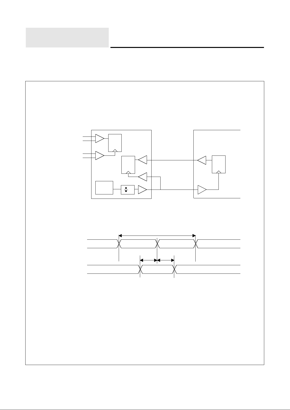
Figure 1: Receive Data and Clock Block Diagram
Figure 2: Receive High Speed Data Input Timing Diagram
RxCLKIN -
RxDATAIN -
RxCLKIN +
RxDATAIN +
QD
CLK
Q
D
CLK
Q D
CLK
CMU
8
VSC8110
PM5355
TXLSCKOUT
TXIN<7:0>
TXLSCKIN
RxCLKIN -
RxDATAIN -
T
RXCLK
RxCLKIN +
RxDATAIN +
T
RXSUTRXH
®
VITESSE Semiconductor Corporation
Page 5
VSC8110
Data Sheet
ATM/SONET/SDH 155/622 Mb/s Transceiv
er
Mux/Demux with Integrated Clock Generation
G51011-0, Rev. 1.5
VITESSE
Table 1: Receive High Speed Data Input Timing Table
(
STS-12 Operation )
Table 2: Receive High Speed Data Input Timing Table
(
STS-3 Operation )
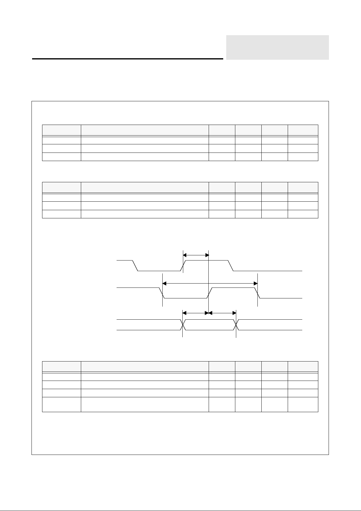
Figure 3: Transmit Data Input Timing Diagram
Table 3: Transmit Data Input Timing Table
(
STS-12 Operation )
Note: Duty cycle for TXLSCKOUT is 50% +/- 5% worse case
Parameter Description Min Typ Max Units
T
RXCLK
Receive clock period - 1.608 - ns
T
RXSU
Serial data setup time with respect to RxCLKIN 500 - - ps
T
RXH
Serial data hold time with respect to RxCLKIN 500 - - ps
Parameter Description Min Typ Max Units
T
RXCLK
Receive clock period - 6.43 - ns
T
RXSU
Serial data setup time with respect to RxCLKIN 1.5 - - ns
T
RXH
Serial data hold time with respect to RxCLKIN 1.5 - - ns
Parameter Description Min Typ Max Units
T
CLKIN
Transmit data input byte clock period - 12.86 - ns
T
INSU
Transmit data setup time with respect to TXLSCKIN 1.0 - - ns
T
INH
Transmit data hold time with respect to TXLSCKIN 1.0 - - ns
T
PROP
Maximum allowable propagation delay for connecting
TXLSCKOUT to TXLSCKIN
- - 3 ns
T
INSU
T
INH
T
CLKIN
TXLSCKIN
TXIN<7:0>
TXLSCKOUT
(1)
T
PROP
VSC8110
VITESSE
Data Sheet
ATM/SONET/SDH 155/622 Mb/s Transceiver
Mux/Demux with Integrated Clock Generation
Page 6 ®
VITESSE
Semiconductor Corporation
G51011-0, Rev. 1.5
Table 4: Transmit Data Input Timing Table
(
STS-3 Operation )
Figure 4: Data and Clock Transmit Block Diagram
Figure 5: Receive Data Output Timing Diagram
Parameter Description Min Typ Max Units
T
CLKIN
Transmit data input byte clock period - 51.44 - ns
T
INSU
Transmit data setup time with respect to TXLSCKIN 1.0 - - ns
T
INH
Transmit data hold time with respect to TXLSCKIN 1.0 - - ns
T
PROP
Maximum allowable propagation delay for connecting
TXLSCKOUT to TXLSCKIN
- - 3 ns
Q
D
CLK
VSC8110
FP
Q D
CLK
QD
CLK
TxDATA
TxCLK
RxDATA
RxCLK
TxCLKOUT -
TxDATAOUT -
TxCLKOUT +
TxDATAOUT +
RXLSCKOUT
RXOUT<7:0>
8
RxCLKIN -
FP
RxCLKIN +
T
PW
T
RXCLKIN
RXLSCKOUT
RXOUT<7:0> A1 A2A2A2
T
RXLSCK
T
SKEW
T
RXVALID
 Loading...