

VITESSE VSC8101QB, VSC8101JA Datasheet
®
VITESSE Semiconductor Corporation
Page 1
VSC8101/8102
Preliminary Data Sheet
155.52 Mb/s Cloc
k and
Data Recovery Units
G52087-0 Rev. 1.3
VITESSE
Features
Functional Description
The VSC8101 and VSC8102 are clock and data recovery units for STS-3 (155.52 Mb/s) applications. They
implement the complete clock and data recovery functions and require no external components. The one-channel device, VSC8101, accepts serial data in NRZ or NRZI format and re-times the data using a sampling clock
extracted from the input data stream. The recovered clock (RCLK+/-) and re-timed data (RDAT+/-) are presented at the serial output ports, aligned such that the falling edge of the recovered clock (RCLK+) coincides
with the center of the data eye (see figure 4). The VSC8102 is an octal version of the VSC8101. A single reference clock input (REFCK+/-) at the STS-3 data rate (155.52MHz) is required for either device. The data and
reference clock inputs, and the recovered data and clock outputs are differential ECL levels referenced to the
V
CC
supply. Only one supply, +2V or -2V, is required for operation.
Both the VSC8101 and VSC8102 employ a digital clock extraction technique, and do not contain a con ventional PLL. As a result, the spectrum of the jitter in the recovered clock and data is non-Gaussian. Peak-to-peak
jitter of RCLK+/- is
±
400 ps or less. The data input rate to the devices is required to be within ± 30 ppm from
the reference clock frequency. The devices have data input jitter accommodation up to 3.2ns, half the data
period. The VSC8101and VSC8102 also provide an input which control the loop bandwidth of the clock extraction function.
Tracking Frequency Bandwidth Control
The tracking of the recovered clock and data to the frequency variation of the input data stream can be
adjusted in the VSC8101 and VSC8102. In particular, the FILTER0 input controls the degree to which the internal clock can track the input data frequency. The effect is equivalent to controlling the loop bandwidth of a conventional PLL-based clock recovery system. Equivalent bandwidths of 150 KHz and 10 KHz can be selected.
The FILTER0 input truth data is shown in the AC Characteristic Table.
Jitter Tolerance
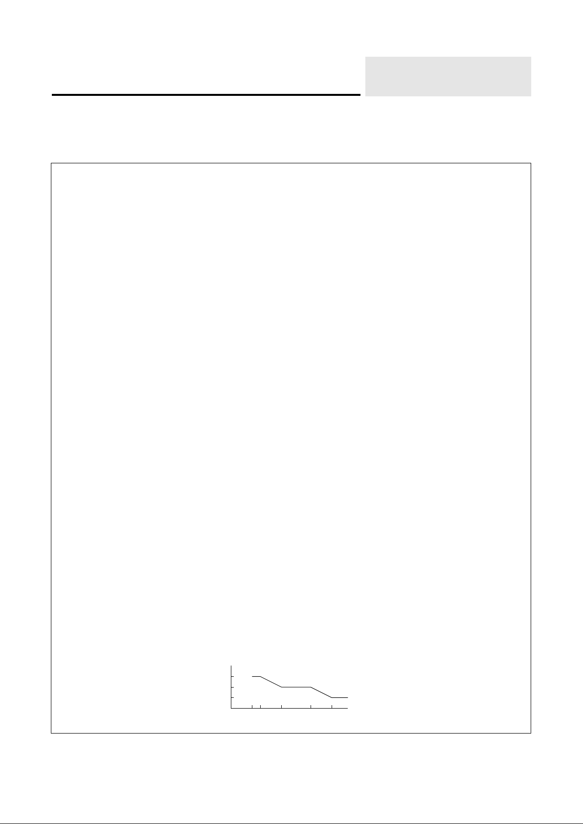
The VSC8101 and VSC8102 are designed to meet the BellcoreGR-253-CORE, section 5.6.2.2.2 Jitter Tolerance specification.
Figure 1: Jitter Tolerance Mask for STS-3
Jitter Amplitude
(UI p-p)
Frequency (Hz)
10 30 300 6.5K 65K
15
1.5
0.15
• Recovers Clock and Data at STS-3 (155.52 Mb/s)
Data Rate.
• No External Components Required.
• Available in One-channel (VSC8101) or
Eight-channel (VSC8102) Versions.
• Recovers Data from NRZ or NRZI Data Streams.
• No Output Clock Drift in Absence of Data
Transitions Once Lock is Acquired.
• ECL or Psuedo ECL (PECL) Differential Inputs
and Outputs.
• Maximum Power Dissipation:
VSC8101: 400mW,
VSC8102: 3W.
• Single 2V Power Supply
• Available in 28PLCC (VSC8101)
and 100PQFP (VSC8102)

VSC8101/8102
VITESSE
Preliminar
y Data Sheet
155.52 Mb/s Clock and
Data Recovery Units
Page 2 ®
VITESSE
Semiconductor Corporation
G52087-0 Rev. 1.3
Figure 2: VSC8101 Block Diagram
Figure 3: VSC8102 Block Diagram
Delay
Digital
Clock
Recovery
SDAT +
SDAT -
RDAT+
RDAT -
RCLK +
RCLK -
Data
Retimer
REFCK +
FILTER0
REFCK -
Delay
Digital
Clock
Recovery
SDAT1 +
SDAT1 -
REFCK +
RDAT1 +
RDAT1 -
RCLK1 +
RCLK1-
FILTER0
Data
Retimer
Delay
Digital
Clock
Recovery
SDAT2 +
SDAT2 -
RDAT2 +
RDAT2 -
RCLK2 +
RCLK2 -
Data
Retimer
Delay
Digital
Clock
Recovery
SDAT8 +
SDAT8 -
RDAT8 +
RDAT8 -
RCLK8 +
RCLK8 -
Data
Retimer
REFCK -
®
VITESSE Semiconductor Corporation
Page 3
VSC8101/8102
Preliminary Data Sheet
155.52 Mb/s Cloc
k and
Data Recovery Units
G52087-0 Rev. 1.3
VITESSE
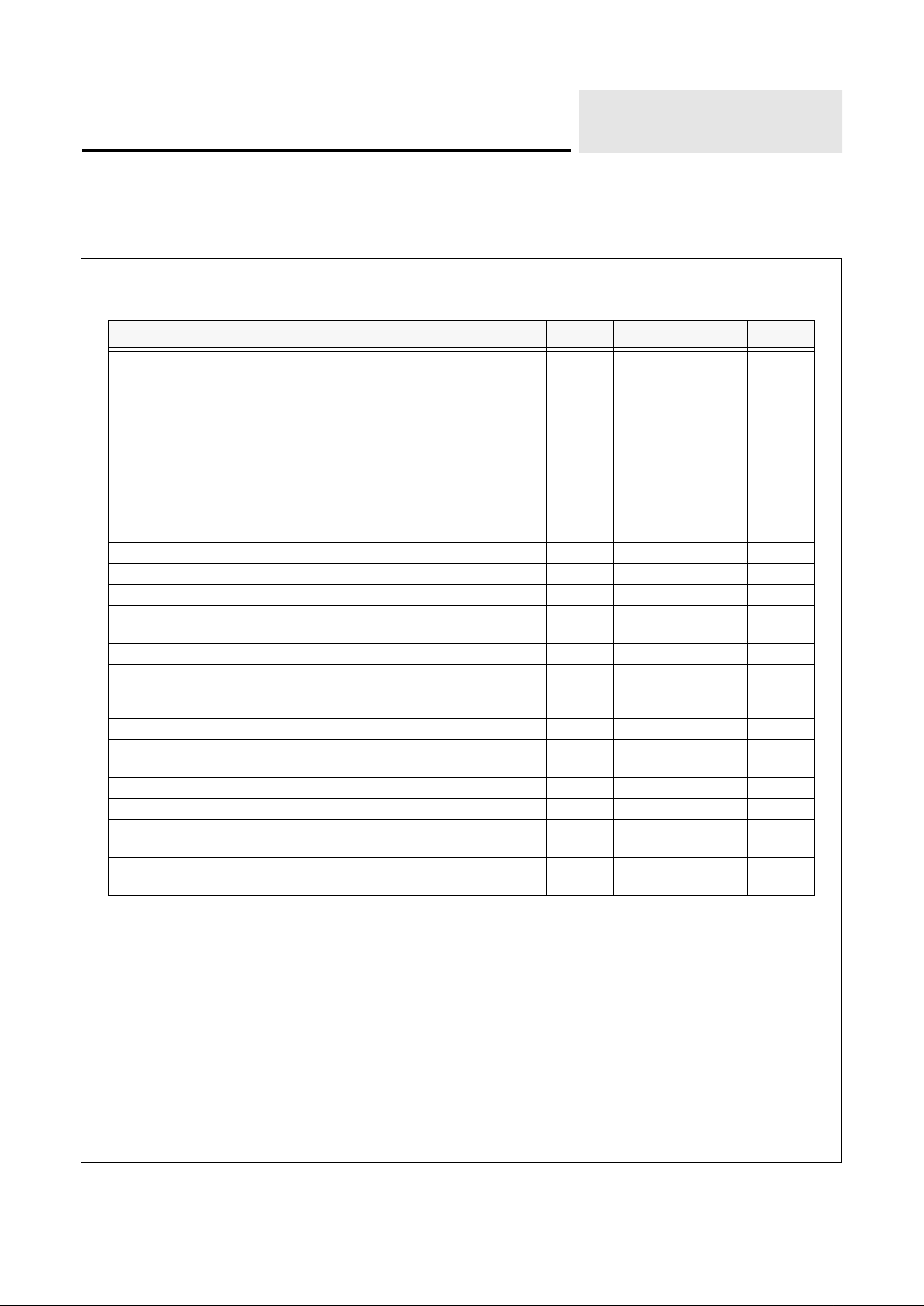
VSC8101/8102 AC Characteristics
(Over recommended operating range
Notes: (1) The part is designed to operate at 155.52 MHz. A reference clock with frequency variation of +/- 50 ppm or better is rec-
ommended. Consult the factory for applications other than this frequency.
(2) With minimum 50% Input Data Eye opening at 155.52 Mb/s.
. (3) With a jitter-free data input and minimum transition density of 50%.
Parameter Description Min Typ Max Units
t
CLK
REFCK+/- Input Clock period
(1)
— 6.43 — ns
t
DCYC
SDAT +/- Input data period
t
CLK
-
30 ppm
—
t
CLK
+
30 ppm
f
DC
SDAT+/- Input Rate Difference with respect to
REFCK+/-
-30 — +30 ppm
t
CDC
REFCK+/- Duty Cycle 40 — 60 %
t
DH
Recovered Data hold time from falling edge of
Recovered Clock
(2)
2.5 — 3.9 ns
t
DS
Recovered Data setup time to falling edge of
Recovered Clock
(2)
2.5 — 3.9 ns
t
RCH
RCLK+/- Recovered Clock Output High Pulse Width 2.6 — — ns
t
RCL
RCLK+/- Recovered Clock Output Low Pulse Width 2.6 — — ns
t
RCYC
RCLK+/- Recovered Clock Period 6.0 — 6.8 ns
t
DJA
SDAT+/- Input Jitter Accommodation (DC to 20 MHz)
Peak-to-peak
— — 3.2 ns
t
LA
Lock Acquisition Time
(3)
— — 5.0 s
f
BW
Loop Bandwidth:
a) at FILTER0 = Lo
b) at FILTER0 = Hi
— — 150
10
KHz
t
RCJ
RCLK+/- Recovered Clock Jitter -400 400 ps
t
PD
Propagation Delay from SDATA+/- Input to RDAT+/Output
— — TBD ps
t
Cr
,
t
Cf
REFCK+/- Input rise and fall time, 20% to 80% — — 1.2 ns
t
SDr
,
t
SDf
SDATA+/- Input rise and fall time, 20% to 80% — — 1.2 ns
t
RCr
,
t
RCf
RCLK+/- Recovered Clock Output rise and fall time,
20% to 80%
300 — 800 ps
t
RDr
,
t
RDf
RDAT+/- Recovered Data Output rise and fall time,
20% to 80%
300 — 800 ps
∆
µ

VSC8101/8102
VITESSE
Preliminar
y Data Sheet
155.52 Mb/s Clock and
Data Recovery Units
Page 4 ®
VITESSE
Semiconductor Corporation
G52087-0 Rev. 1.3
Figure 4: VSC8101/8102 AC Timing Waveform
Absolute Maximum Ratings
(1)
Power Supply Voltage ( V
CC
-
V
TT
)..................................................................................................-0.5V to +3.0V
Input Voltage (
V
IN
) ...................................................................................................... V
CC
-2.5V to V
CC
+ 0.5V
Output Current,
I
OUT
(DC, Output HI) .......................................................................................................-50mA
Case Temperature Under Bias,
T
C
................................................................................................. -55 ° to +125 ° C
Storage Temperature (
T
STG
)........................................................................................................-65 ° C to +135 ° C
Recommended Operating Conditions
The VSC8101 and VSC8102 can be powered by:
a) connecting
V
CC
to +2V and V
TT
to GND, or
b) connecting
V
CC
to GND and V
TT
to -2V.
Power Supply Voltage (
V
CC
-
V
TT
)........................................................................................................ 2.0V ± 5%
Operating Temperature Range
(2)
........................................................................................................ 0 ° to +70 ° C
Notes:
(1) CAUTION: Stresses listed under “Absolute Maximum Ratings” may be applied to devices one at a time without causing pe
manent damage. Functionality at or above the values listed is not implied. Exposure to these values for extended periods
may affect device reliability.
(2) Lower limit is ambient temperature and upper limit is case temperature.
VALID DATA (0)
VALID DATA (1)
t
DH
t
DS
t
RCYC
Reference Clock
REFCK+ / REFCK-
t
CLK
RCLK+ / RCLK-
Recovered Clock
RDAT+ / RDAT-
Recovered Data
DATA IN (1) DATA IN (2)
SDAT+ / SDAT-
t
DCYC
t
RCL
t
RCH
VALID DATA (2)
t
PD
Input Data
t
DJA
Note: (1) Solid line indicates the true sense and dotted line indicates the complementary sense of the signal.
(1)
(1)

®
VITESSE Semiconductor Corporation
Page 5
VSC8101/8102
Preliminary Data Sheet
155.52 Mb/s Cloc
k and
Data Recovery Units
G52087-0 Rev. 1.3
VITESSE
VSC8101/8102 DC Characteristics
(Over recommended operating conditions)
Table 1: Inputs and Outputs
Parameter Description Min Typ Max Units Conditions
V
IH
Input HIGH voltage
V
CC
-
1150
—
V
CC
-
600
mV
Guaranteed HIGH signal for all
inputs
V
IL
Input LOW voltage V
TT
—
V
CC
-
1500
mV
Guaranteed LOW signal for all
inputs
V
OH
Output HIGH voltage
V
CC
-
1020
—
V
CC
-
700
mV
VIN = VIH (max) or VIL (min).
Outputs terminated identically into
V
TT
with 50 ohms.
V
OL
Output LOW voltage V
TT
—
V
CC
-
1620
mV
VIN = VIH (max) or VIL (min).
Outputs terminated identically into
V
TT
with 50 ohms.
V
I
Input voltage swing for
REFCK+/- and SDAT+/-
450 — — mV
(1) For AC-Coupling: input swing
at the pin.
(2) For DC-Coupling: input swing
referenced to the common mode
voltage;
V
OCM
Output common mode
voltage for RDAT+/- and
RCLK+/-
.5 +
V
TT
—
.8 +
V
TT
Differential Outputs terminated
identically into VTT with 50 ohms.
V
O
Output voltage swing for
RDAT+/- and RCLK+/-
600 — — mV
Differential Outputs terminated
identically into VTT with 50 ohms.
Table 2: Power Dissipation
Parameter Description Min Typ Max Units Conditions
P
D
Power dissipation
(VSC8101)
— — 400 mW Outputs open, VCC = 2.1V
P
D
Power dissipation
(VSC8102)
— — 3.0 W same as above
I
CC
Supply current (VSC8101) — — 190 mA same as above
I
CC
Supply current (VSC8102) — — 1430 mA same as above
∆
∆
 Loading...