

VITESSE VSC8022FC, VSC8021FI, VSC8021FC, VSC8022FI Datasheet

Data Sheet
VSC8021/VSC8022
Features
• Serial Data Rates up to 2.5Gb/s
VITESSE
SEMICONDUCTOR CORPORATION
2.5Gb/s SONET-Compatible
8-Bit MUX/DEMUX Chipset
• Differential or Single-Ended Inputs and Outputs
• Parallel Data Rates up to 312.5Mb/s
• ECL 100K Compatible Parallel Data I/Os
• Divide-by-8 Clock for Synchronization of
Parallel Data to Interfacing Chips
• SONET Frame Recovery Circuitry
(VSC8022)
• Compatible with STS-3 to STS-48
SONET Applications
• Low Power Dissipation: 2.3W (Typ Per Chip)
• Standard ECL Power Supplies:
V
= -5.2V, VTT = -2.0V
EE
• Available in Commercial (0
(-40
°C to +85°C) Temperature Ranges
• Proven E/D Mode GaAs Technology
• 52-Pin Leaded Ceramic Chip Carrier
°C to +70°C) or Industrial
Functional Description
The VSC8021 and VSC8022 are high-speed SONET interface devices capable of handling serial data at
rates up to 2.5Gb/s. These devices can be used for STS-3 through STS-48 SONET applications.
These products are fabricated in gall ium arsenide usi ng the Vitesse H-GaAs
achieves high-speed and low power dissipation. These products are packaged in a ceramic 52-pin leaded
ceramic chip carrier.
E/D MESFET process which
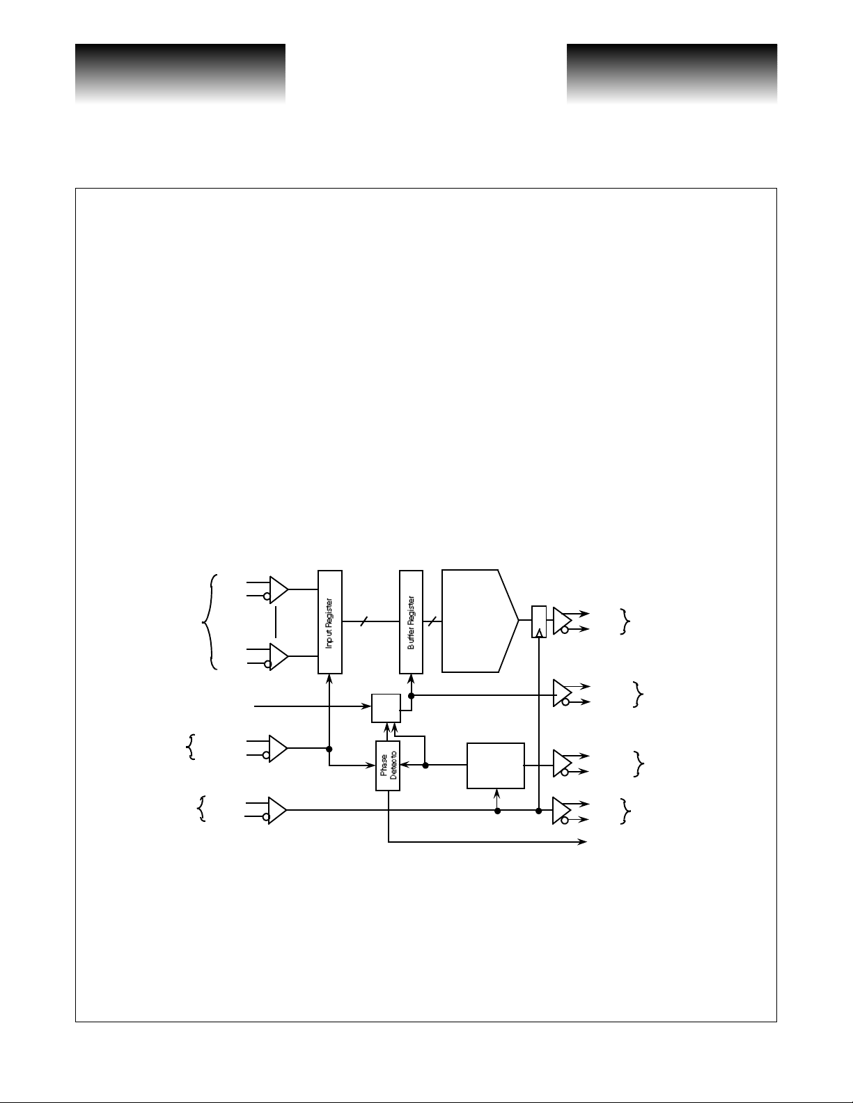
VSC8021
The VSC8021 contain s an 8: 1 multiplexer and a self-positioni ng t ime r. The 8:1 multip lex er ac cept s 8 parallel differential ECL data inputs (D1-D8, D1N-D8N) at rates up to 312.5Mb/s and multiplexes them into a serial
differential bit stream output (DO, DON) at rates up to 2.5Gb/s.
The internal timing of the VSC8021 is built around the high-speed clock (up to 2.5GHz) delivered onto the
chip through a differential input (CLKI, CLKIN). Thi s si gnal i s subsequently echoed at the high-speed differential output (CO, CON).
The parallel data inputs are clocked to on-chip input registers with an externally supplied differential ECL
input (BYCLK, BYCLKN) operating at the same rate as the data inputs. An internal byte clock, which is a
divide-by-8 version of the high-speed clock, is used to transfer the data to a set of buffer registers. This internal
byte clock is brought off chip at the ECL output CLK8, CLK8N.
Internal circuitry monitors the in ternal and ext ernal byte cloc ks and gene rates an ERR sign al if a timing
violation is detected. Thi s sign al ca n be gated to the SYNC input which is edge sensitive high. An active SYNC
input allows the VSC8021 timing to shift, positioning it properly against the external byte clock, CLK8,
CLK8N. When a CLK8 timing switch is made, normal data flow will be invalid for 1 byte.
There are two clock inputs, CLKI and BYCLK, going into the VSC8021. These two clocks serve as timing
references for different parts of the VSC8021. The BYCLK is used to trigger the input registers for the parallel
data inputs, while the CLKI is used to trigger the high-speed serial output register as well as some of the timing
circuitry for the parallel to serial conversion. Furthermore, in order to make this part easy to use, the user is not
required to assume a known phase relationship between CLKI and the BYCLK.
G52028-0, Rev 4.1 Page 1
05/25/01
© VITESSE SEMICONDUCTOR CORPORATION • 741 Calle Plano • Camarillo, CA 93012
Tel: (800) VITESSE • FAX: (805) 987-5896 • Email: prodinfo@vitesse.com
Internet: www.vitesse.com
VITESSE
Phase
Adjust
SEMICONDUCTOR CORPORATION
2.5Gb/s SONET-Compatible
8-Bit MUX/DEMUX Chipset
VSC8021/VSC8022
Data Sheet
An internal Phase Detector and Phase Adjust Circuit are used to facilitate the two asynchronous circuits to
work with each other. The Phase Detector and the Phase Adjust Circuit work together to adjust the internal
clock CLK8 to make sure the set up and hold conditions are met for the inter nal regi sters. CLK8 is derived from
CLKI and the RCLK is a non-phase varying byte clo ck output. The edge sensitiv e SYNC signal is simply the
control signal that enables the Phase Detector circuitry.
As a summary, the CLKI is the high-speed clock input. The BYCLK is the external byte clock. The CLK8
is the internal byte clock deriv ed from C LKI, phase-adjusted if SYNC is enabled. The RCLK is a no n-phaseadjusted divided-by-8 clock generated from CLKI. The phase of RCLK, RCLKN is not affected by the selfadjusting circuitry, therefore it can be used as a system reference cl ock . RCLK, RCLKN can be use d by the system designer to generate BYCLK, BYCLKN. The self-posit i oni ng timer and R CLK, RCLKN allow for the creation of very tight parallel data timing for the VSC8021.
Figure 1: VSC8021 Block Diagram
Parallel
Byte Clock
Inputs
High Speed
Clock Inputs
Data
D1N
D8N
SYNC
BYCLK
BYCLKN
CLKI
CLKIN
D1
D8
8 8
8:1
Multiplexer
Timing
Generator
DO
DON
CLK8
CLK8N
RCLK
RCLKN
CO
CON
ERR
Serial Data Output
Phase Adjustable
Byte Clock Output
Independent
Byte Clock Output
High Speed
Clock
Page 2 G52028-0, Rev 4.1
© VITESSE SEMICONDUCTOR CORPORATION • 741 Ca l le Pl an o • Camarillo, CA 93012
Tel: (800) VITESSE • FAX: (805) 987-5896 • Email: prodinfo@vitesse.com
Internet: www.vitesse.com
05/25/01
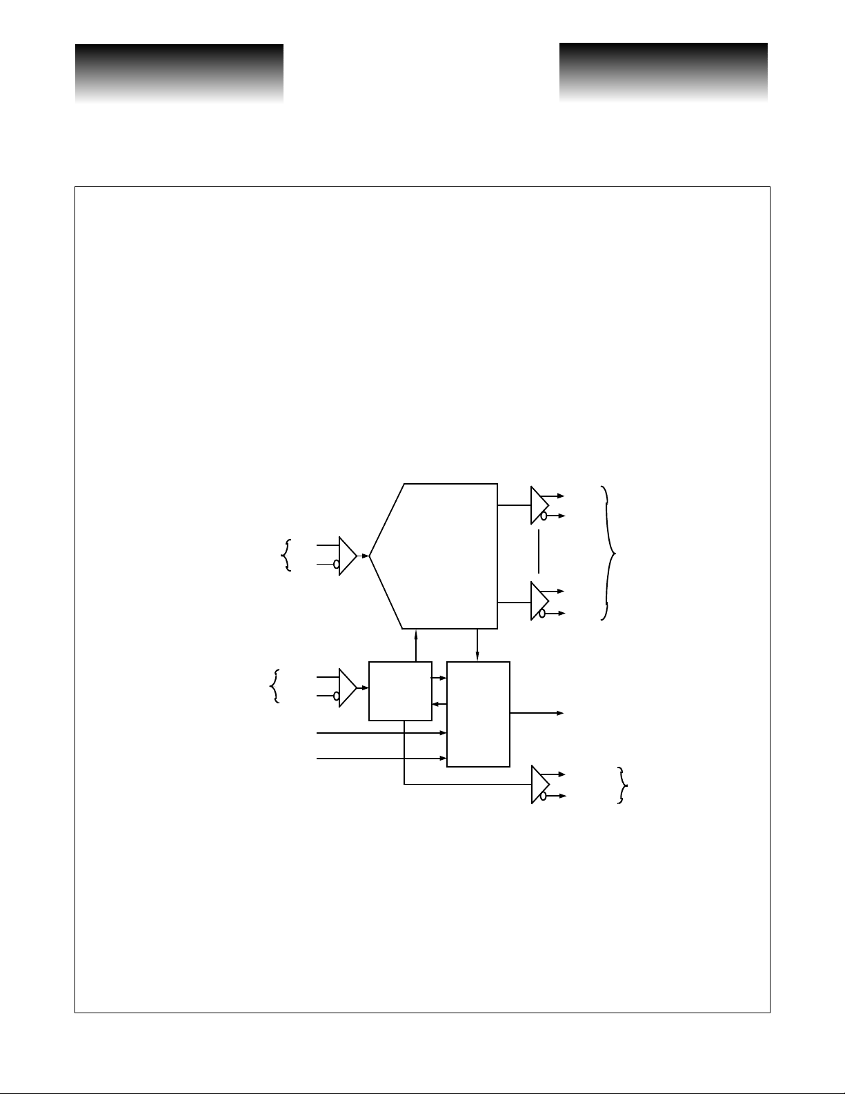
VITESSE
Frame Recovery Disable —
Frame Recovery Clock —
SEMICONDUCTOR CORPORATION
Data Sheet
2.5Gb/s SONET-Compatible
VSC8021/VSC8022
VSC8022
The VSC8022 cont ains bot h a 1:8 demu ltiplex er and SON ET frame re covery c ircuitry. The 1:8 demult iplexer
accepts a serial data input (
(
D1-D8, D1N-D8N) at rates up to 312.5Mb/s. Valid parallel data outputs are indicated by the divide by 8 differential
clock outputs
The VSC8022 also contains a SONET frame recovery circuit. The frame recovery circuits are enabled by a falling edge on the
ing for the SONET framing sequence. Once the frame is detected, the word boundary is realigned, a confirmation
signal is sent off-chip through the
aligner is hunting for the frame,
BYCKO, BYCKON.
OOFN ECL input when the FDIS input is low. Once enabled, the frame recovery circuit starts look-
DI, DIN) at rates up to 2.5Gb/s and converts it into 8 parallel differential ECL data outputs
FP ECL output and the frame rec overy circuits are di sabled. While the fra me
BYCKO, BYCKON and parallel data are invalid.
Figure 2: VSC8022 Block Diagram
8-Bit MUX/DEMUX Chipset
D1
D1N
Serial Data In
High Speed
Clock Inputs
Frame recovery circuits are disabled by frame detection (resulting in FP) or by a falling edge on the OOFN
input while FDIS is high.
DIN
CLKI
CLKIN
FDIS
OOFN
DI
Generator
Demultiplexer
Timing
1:8
SONET
Frame
Detection &
Recovery
Parallel
Data Outputs
D8
D8N
— Frame Detect i on S i gnal
FP
BYCKO
BYCKON
Byte Clock Out
G52028-0, Rev 4.1 Page 3
05/25/01
© VITESSE SEMICONDUCTOR CORPORATION • 741 Calle Plano • Camarillo, CA 93012
Tel: (800) VITESSE • FAX: (805) 987-5896 • Email: prodinfo@vitesse.com
Internet: www.vitesse.com
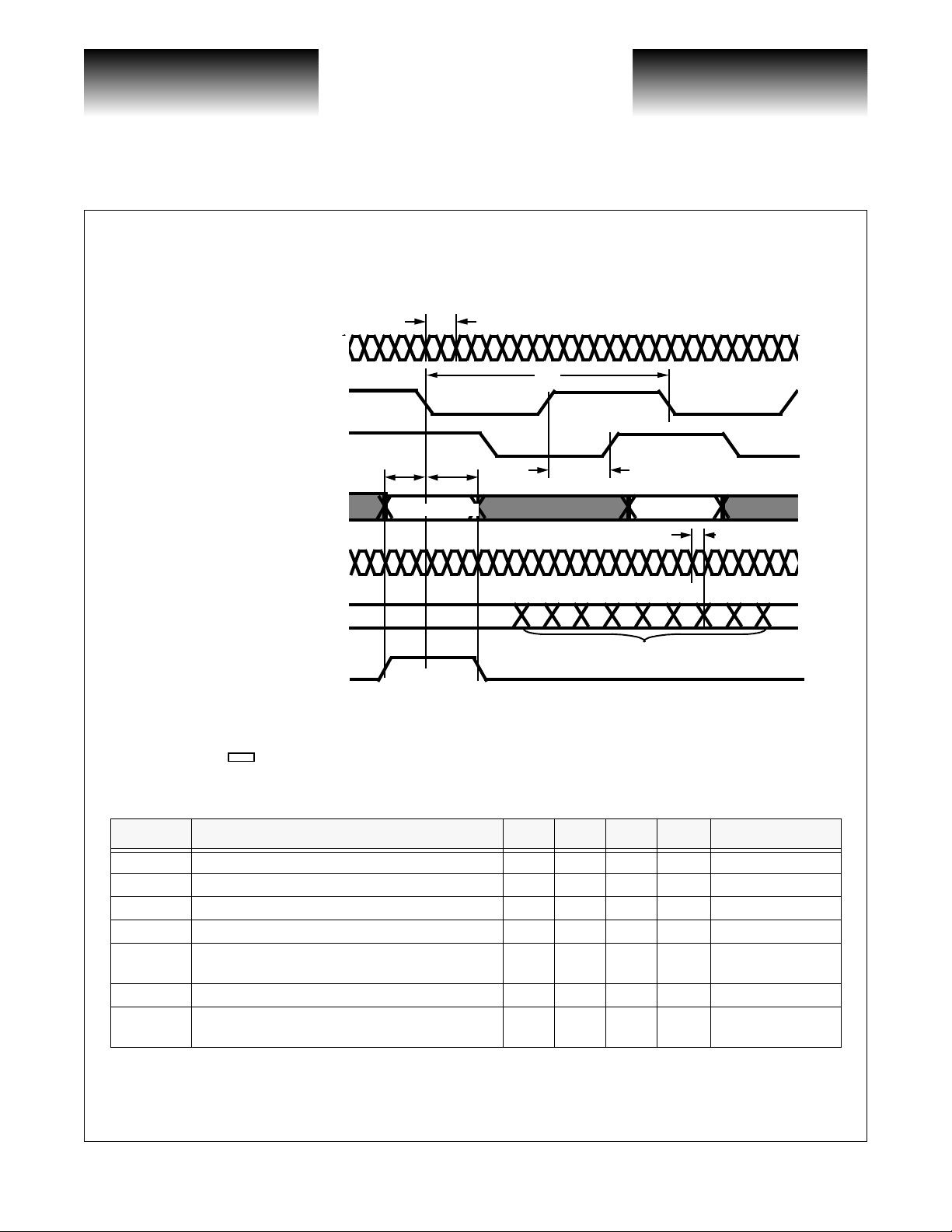
VITESSE
t
C
t
DH
CO, CON
DO,DON
Byte clock input
Parallel differential data inputs
CLK8 adjustment input
Phase adjustable ÷8 output
SEMICONDUCTOR CORPORATION
2.5Gb/s SONET-Compatible
8-Bit MUX/DEMUX Chipset
VSC8021/VSC8022
VSC8021 Multiplexer AC Characteristics (Over recommended operating conditions)
Figure 3: VSC8021 Multiplexer Waveforms
(1)
CLKI , CLKIN
High speed differential clock input
BYCLK (BYCLKN)
(1)
CLK8
D1-D8, D1N-D8N
High speed differential clock outputs
(2)
t
DSU
VALID DATA(1)
t
D
t
BCLK8
VALID DATA(2)
t
CMD
Data Sheet
High speed differential data outputs
SYNC
(1) Negative edge is active edge.
NOTES:
(2) BYCLK/CLK8 timing required when SYNC not connected to ERR.
period x 8 = period.CLKI (CLKIN) BYCLK (BYCLKN)
= Don’t care.
T able 1: VSC8021 Multiplexer AC Characteristics
(over recommended operating conditions)
D01 D02 D03 D04 D05 D06 D07 D08
Serialized Byte 1
Parameter Description Min Typ Max Units Conditions
t
C
t
D
t
DSU
t
DH
t
CMD
t
BCLK8
Jitter (p-p)
NOTES: (1) The parts are guaranteed by design to operate from DC to a maxim um f requency of 2.5GHz.
Clock period
BYTE clock period (tD = tC x 8) 3.2 ns
Parallel data set-up time 0.6 ns
Data hold time 1.4 ns
High-speed clock output (CO, CON) timing, falling
edge of CO to muxed data output, (DO, DON) timing
Byte clock to CLK8 timing
CLKI, CLKIN to DO, DON (max-min), (HI to LO),
same part, same pin at constant conditions
(2) Required when SYNC not connected to ERR.
(1)
(2)
400 ps
220 350 ps
0.5 1.0 1.5 ns
<50 ps
Page 4 G52028-0, Rev 4.1
© VITESSE SEMICONDUCTOR CORPORATION • 741 Ca l le Pl an o • Camarillo, CA 93012
Tel: (800) VITESSE • FAX: (805) 987-5896 • Email: prodinfo@vitesse.com
Internet: www.vitesse.com
05/25/01
05/25/01
Tel: (800) VITESSE • FAX: (805) 987-5896 • Email: prodinfo@vitesse.com
G52028-0, Rev 4.1 Page 5
© VITESSE SEMICONDUCTOR CORPORATION • 741 Calle Plano • Camarillo, CA 93012
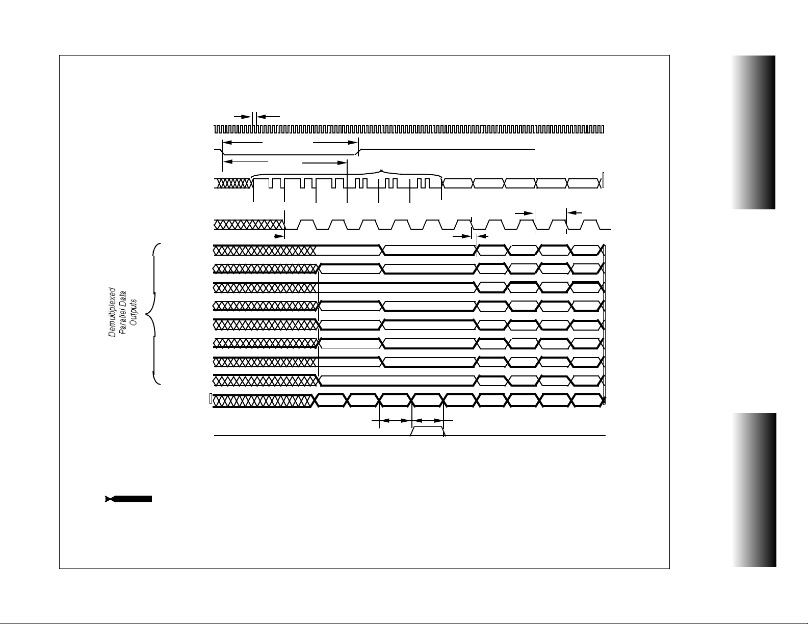
(1)
High speed differential clock input
Frame reco ve ry clo c k in p u t
High speed serial data inputs
CLKI (CLKIN)
OOFN
DI (DIN)
BYCKO (BYCKON)
Byte clock output
D1 (D1N)
t
C
t
OOFNPW
t
OOFN
A1 A1 A1 A2 A2 A2
ResynchBYCKO
SONET STS-3 Framing Sequence
DATA
DATA DATA DATA DATA
t
D
t
BD
Valid D ata Valid Data
Data Sheet
VSC8021/VSC8022
VSC8022 AC Characteristics (Over recommended operating conditions)
Figure 4: VSC8022 Demultiplexer Waveforms
VITESSE
SEMICONDUCTOR CORPORATION
Internet: www.vitesse.com
Output Summary
Frame detection confirm output
NOTES:
1) Negative edge is active edge.
2) The parallel data outputs only begin showing valid data after the last A2 of the SONET framing sequen ce. Th e exam ple
waveforms shown above use an STS-3 framing sequence for convenience, thus valid data is output after the third
A2 in the sequence.
= Don’t care.
D2 (D2N)
D3 (D3N)
D4 (D4N)
D5 (D5N)
D6 (D6N)
D7 (D7N)
D8 (D8N)
Parallel Data•
(2)
FP
t
DFP
A1A1
A2 A2 A2
Valid Data Valid Data
Valid Data Valid Data
Valid Da ta Valid Data
Valid Da ta Valid Data
Valid Data Valid Data
Valid Da ta Valid Data
Valid Da ta Valid Data
Data Data Data Data
t
PFP
2.5Gb/s SONET-Compatible
8-Bit MUX/DEMUX Chipset
VITESSE
SEMICONDUCTOR CORPORATION
2.5Gb/s SONET-Compatible
8-Bit MUX/DEMUX Chipset
T a ble 2: VSC8022 Demultiplexer AC Characteristics
Parameter
t
C
t
D
t
BD
t
DFP
t
PFP
t
OOFN
t
OOFNPW
Phase
Margin
NOTE: (1) If tC changes, all the remaining parameters change as indicated by the equations.
Clock period
BYTE clock period (tD = tC x 8) (framed) 3.2 ns
BYTE clock output to valid data 0.5 1.0 2.0 ns
FP rising edge from parallel data output
change from A1 to A2 (t
FP pulse width ( t
OOFN falling edge before A1 chan
ges to A2 (t
OOFN pulse width (t
Serial data phase timing margin with respect
to high-speed clock:
Phase Margin =
Description Min Typ Max Units Conditions
(1)
= tD)
DFP
= tD)3.2 ns
PFP
= tD x 4)
OOFN
OOFNPW
+
t
SUtH
1
-------------------–
t
C
= tD)3.2 ns
360°
400 ps
3.2 ns
12.8 ns
135 180 degrees
Data Sheet
VSC8021/VSC8022
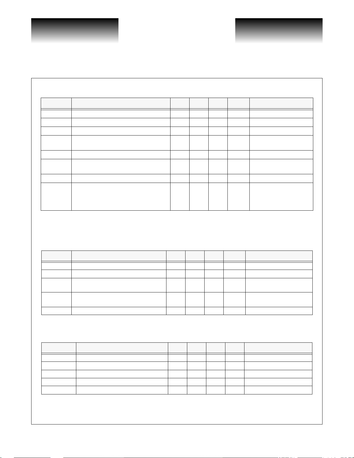
DC Characteristics
Table 3: Low Speed ECL Inputs and Outputs
(Over recommended operating range with internal V
Parameter
V
OH
V
OL
V
IH
V
IL
∆V
OUT
Note: Differential ECL output pins must be terminated identically.
Output HIGH volta ge -1020 -700 mV VIN = VIH (max) or VIL (min)
Output LOW voltage V
Input HIGH voltage -1150 -600 mV
Input LOW voltage V
Output voltage swing 0.8 1.0 1.4 V Output load 50Ω to V
Description Min Typ Max Units Conditions
Table 4: High-Speed Inputs and Outputs
(Over recommended oper at ing conditions, V
Parameter
∆V
IN
V
OH
V
OL
∆V
OUT(DATA)
∆V
OUT(clk)
NOTES: (1) A reference genera tor is built in to each high- s peed input, and these inp uts are designed t o be AC -coupled.
(2) If a high-speed input is used single-ended, a 150pF capacitor must be connected between the unused high-speed or comple-
ment input and the po wer supply (VTT).
(3) Differential high-speed outputs must be terminated iden tically.
Input voltage swing 0.8 1.0 1.2 V AC-coupled
Output HIGH voltage -0.9 V Output load, 50Ω to -2.0V
Output LOW voltage -1.8 V Output load, 50Ω to -2.0V
Output voltage swing for data 0.6 0.8 1.2 V Output load, 50Ω to -2.0V
Output voltage swing for clock 0.6 0.7 1.2 V Output load, 50Ω to -2.0V
Description Min Typ Max Units Conditions
= GND, Output load = 50Ω to -2.0V)
CC
= GND, output load = 50Ω to -2.0V)
REF, VCC
TT
TT
-1620 mV VIN = VIH (max) or VIL (min)
Guaranteed HIGH signal for
all inputs
-1500 mV
Guaranteed LOW signal for
all inputs
TT
Page 6 G52028-0, Rev 4.1
© VITESSE SEMICONDUCTOR CORPORATION • 741 Ca l le Pl an o • Camarillo, CA 93012
Tel: (800) VITESSE • FAX: (805) 987-5896 • Email: prodinfo@vitesse.com
Internet: www.vitesse.com
05/25/01
 Loading...