

VITESSE VSC7991X, VSC7991CD Datasheet
VITESSE
SEMICONDUCTOR CORPORATION
Advance Product Information
VSC7991
Electroabsorption Modulator/Laser Diode Driver
SONET/SDH 10.7Gb/s
Features
• Maximum Rise/Fall Times of 38ps
• High-Speed Operation
(Up to 10.7Gb/s NRZ Data)
• Differential Inputs
• Single-Supply
• CML-Compatible Data Inputs
• On-Chip 50Ω Input Terminations
• 50Ω Output Impedance
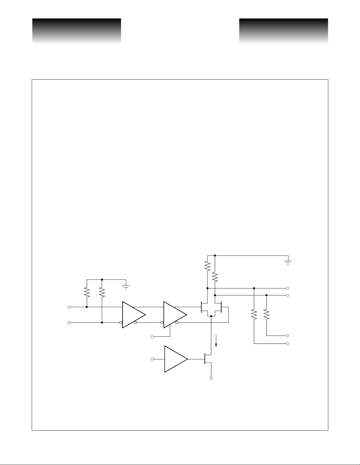
General Description
The VSC7991 is a single 7V supply, 10.7Gb/s Electroabsorption Modulator (EAM)/laser diode driver with
direct access to the laser modulation FETs. Laser offse t and modul at ion current s are set by external comp onent s
allowing precision moni t ori ng and setting of the voltage leve ls. Data inputs are differenti al ly t er min ated to 50Ω.
Applications
• SONET/SDH @ 2.488Gb/s, 9.952Gb/s, 10.7Gb/s
VSC7991 Block Diagram
(1)
50Ω
DIN
NDIN
Note: (1) On-die components.
50Ω
(1)
60Ω
(1)
60Ω
(1)
DCC
VIP
(1)
300Ω
I
MOD
IP
300Ω
NDOUT
DOUT
(1)
IB
IBN
G52321-0, Rev 2.3 Page 1
02/26/01
© VITESSE SEMICONDUCTOR CORPORATION • 741 Calle Plano • Camarillo, CA 93012
Tel: (800) VITESSE • FAX: (805) 987-5896 • Email: prodinfo@vitess e.com
Internet: www.vitesse.com
VITESSE
SEMICONDUCTOR CORPORATION
SDH/SONET 10.7Gb/s
Advance Product Information
Electroabsorption Modulator/Laser Diode Driver
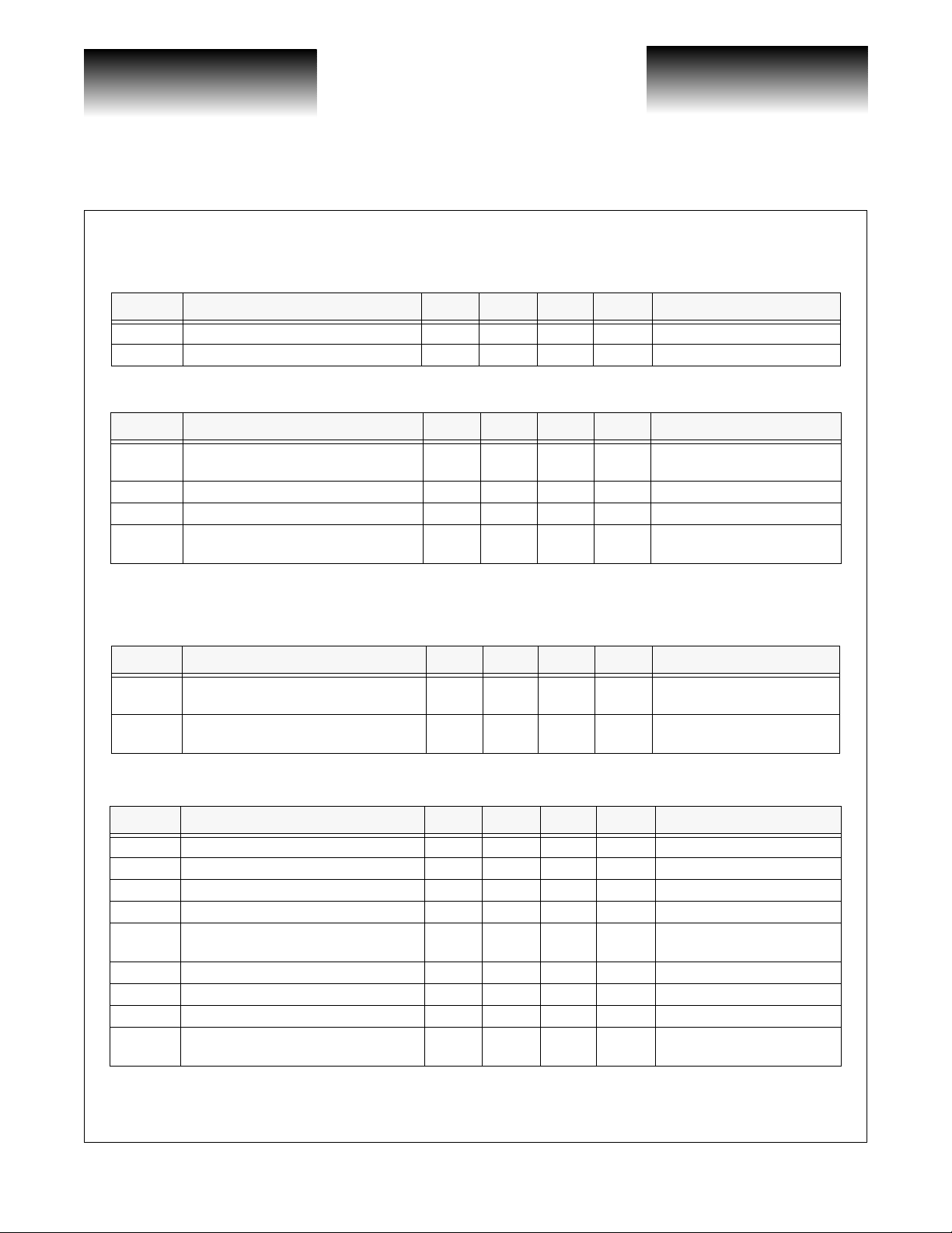
AC Characteristics (Over recommended operating conditions)
Table 1: High Speed Inputs /Outputs
Symbol Parameter Min Typ Max Units Conditions
IRL Input Return Loss, 50Ω System −15 dB 50MHz to 10GHz
ORL Output Return Loss, 50Ω System
−12 dB 50MHz to 10GHz
T able 2: Laser Driver AC Electrical Specifications
Symbol Parameter Min Typ Max Units Conditions
tR t
F
Jitter Output Jitter 15 ps/p-p 50Ω Load, V
Output Rise and Fall Times 38 ps
Overshoot/Undershoot −10 +10 %
Duty-Cycle −25 +25 %
50Ω load, 20% to 80%, V
= 3V
DCC in the range of V
0.5V to V
DC Characteristics (Over recommended operating conditions)
Table 3: Power Dissipation
VSC7991
= 3V
MOD
SS
SS
+2V
MOD
−
Symbol Parameter Min Typ Max Units Conditions
= −6.8, RL = 50Ω to GND,
V
I
P
VSS
D
Power Supply Current (V
Total Power Dissipation 2040 2244 mW
) 300 330 mA
SS
SS
I
= 120mA, V
MOD
= −6.8, RL = 50Ω to GND
V
SS
= 120mA, V
I
MOD
BIAS
BIAS
= 0V
= 0V
T able 4: Laser Driver DC Electrical Specifications
Symbol Parameter Min Typ Max Units Conditions
V
BIAS
V
MOD
V
OCM
IB, IBN L aser Bias Control Voltage −10 0V
V
IP
V
IH
V
IL
V
SW
DCC Duty-Cycle Control
NOTE: DIN and NDIN inputs need to be driven di ff erentially. If single-ended drive is desired, it is necessary to add a DC bias to the unused pin.
Programmable Output Offset Voltage −0.8 0V
Modulation Voltage Amplitude 1.5 3V
Output Voltage Compliance 4 V
Laser Modulation Control Voltage V
Input High Voltage −150 0mV
Input Low Voltage −1.00 −0.60 V
(1)
Input Voltage Swing 450 1000 mVp-p
SS
VSS −
0.5V
VSS +
0.7
VSS+
2V
V
Page 2 G52321-0, Rev 2.3
© VITESSE SEMICONDUCTOR CORPORATION • 741 Calle Plano • Camarillo, CA 93012
Tel: (800) VITESSE • FAX: (805) 987-5896 • Email: prodinfo@vitesse.com
Internet: www.vitesse.com
02/26/01
VITESSE
SEMICONDUCTOR CORPORATION
Advance Product Information
VSC7991
Absolute Maximum Ratings
Negative Power Supply Voltage (VSS)..............................................................................................VCC to −8.0V
All Pins............................................... ........ ................................................................ .........................V
Supply Voltage (V
Supply Current (I
Input Voltage (V
Output Voltage (V
Modulation Control Voltage (V
Output Offset Control Voltage (IB, IBN)..........................................................................................................11V
Output Offset Control Current (I
Maximum Junction Temperature Range .....................................................................................−55°C to +125°C
Storage Temperature Range: .......................................................................................................−55°C to +125°C
Note:
(1) CAUTION: Stresses listed under “Absolut e Maximum Ratings” may be applied to devices one at a time without causing per-
manent damage . Fu nctionality at or above th e va lues listed is not implied . Ex p os u re to these values fo r ex te nd e d p e r iod s m ay
affect device reliability.
) ......................................................................................................................................... 8V
SS
)....................................................................................................................................500mA
SS
)........................................................................................................................................−2.0V
IN
)................................................................................................................................. −4.0V
OUT
).........................................................................................................VSS − 0.5V
IP
) .............................................................................................................. 50mA
IB
(1)
Electroabsorption Modulator/Laser Diode Driver
SONET/SDH 10.7Gb/s
SS
Recommended Operating Conditions
Positive Voltage Rail (GND).............................................................................................................................. 0V
Negative Voltage Rail (V
Operational Case Temperature (T
)...........................................................................................................−6.5V to −7.2V
SS
) ...................................................................................................0°C to 75°C
C1
to + .5V
G52321-0, Rev 2.3 Page 3
02/26/01
© VITESSE SEMICONDUCTOR CORPORATION • 741 Calle Plano • Camarillo, CA 93012
Tel: (800) VITESSE • FAX: (805) 987-5896 • Email: prodinfo@vitesse.com
Internet: www.vitesse.com
 Loading...