

VITESSE VSC7969YD2, VSC7969WD2B, VSC7969YD1, VSC7969WD2A, VSC7969WD1B Datasheet
...
VITESSE
SEMICONDUCTOR CORPORATION
Advance Product Information
VSC7969
3.125Gb/s Integrat ed Transim p eda nce
and Limiting Amplifier with Signal Detect
Features Applications
• Integrated TIA and Limiting Amplifier
• Low Power Consumption for SFF Applications
• TO Package-Compatible Layout
• On-Chip Signal Detect
• On-Chip Linear Photocurrent Monitor
• Single 3.3V Supply
• 5V Supply Operation via Wirebond Option
• Compatible with PIN or Avalanche Detectors
• Packages: 16-Pin TSSOP, TO-46, Bare Die
• 2.488Gb/s, 3.125Gb/s SONET OC-48/
SDH STM-16
• 2.125Gb/s Fibre Channel
• 2.5Gb/s or 3.125Gb/s Ethernet Applications with
8B/10B Overhead
• SFF Transceivers
General Description
The VSC7969 is a 3.125Gb/s transimpedance amplifier IC with a built-in limiting amplifier, a signal detect
feature and a photocurrent monitor. The VSC7969 does not require any external electrical components in the
construction of a high performance optical receiver such as for SONET/SDH applications. The analog output is
a differential sig nal with a min imum amplitude of 200mVp-p ( singl e-ended). The VSC7969 opera tes with a single power supply with a maximum power dissipation of 300mW. A PIN photodiode or APD can be connected
and separately biased to provide optimal performance.
The VSC7969 provides filt ered bias f or MSM and PIN phot odete ctors; appli cations u sing an APD ph otodetector must supply bias separately. The VSC7969 also provides a photocurrent monitor whose output is linearly
proportional to the input photocurrent.
The VSC7969 can operate from a single +3.3V supply or a +5V or -5.2V supply. The VSC7969 is offered
in die form and in a 16-pin plastic thin-shrink small outline package (TSSOP-16). A fully tested TO-46 outline
packaged receiver with a photodetector is also available.
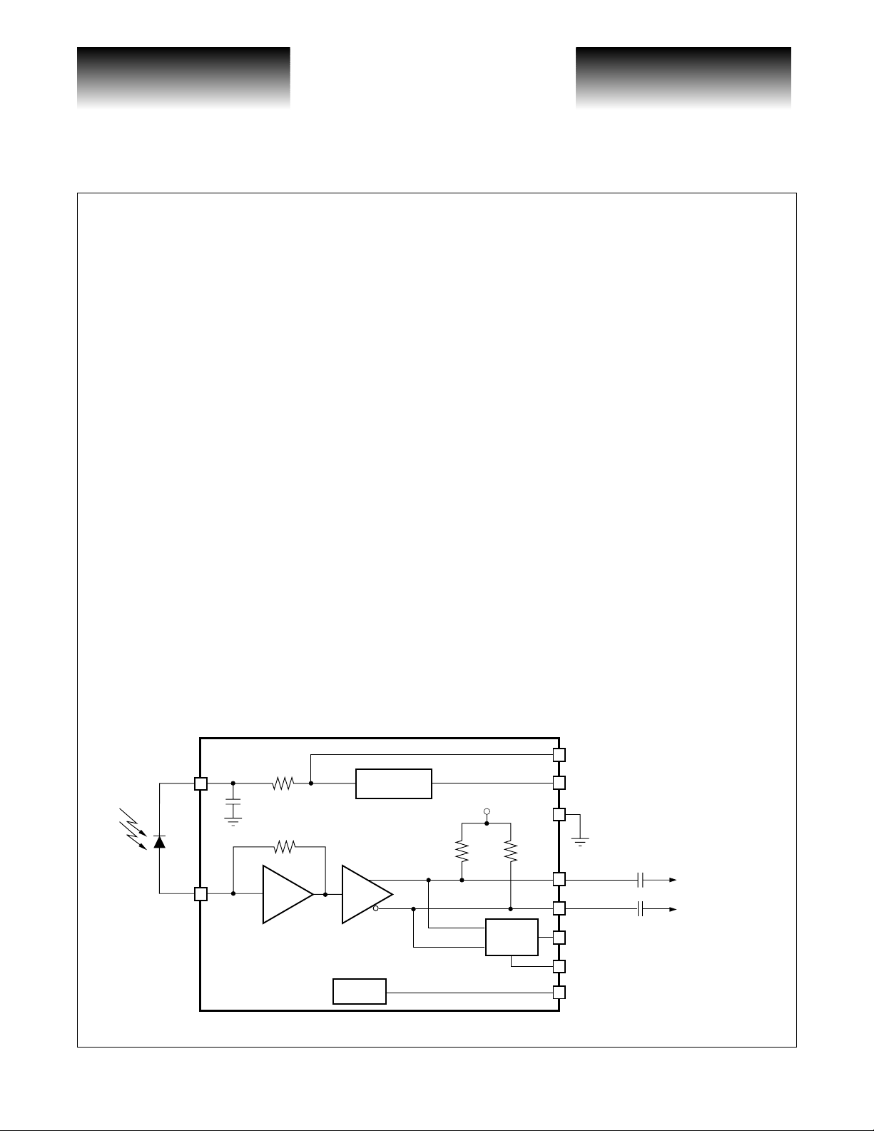
Block Diagram
Dual power supply pins are
VCCS
provided for +5V or +3.3V
Filter
In
VSC7969
G52355-0, Rev 2.0 Page 1
02/09/01
© VITESSE SEMICONDUCTOR CORPORATION • 741 Calle Plano • Camarillo, CA 93012
Tel: (800) VITESSE • FAX: (805) 987-5896 • Email: prodinfo@vitesse.com
+3.3V +5V
Regulator
50Ω
Monitor
Internet: www.vitesse.com
+3.3V
50Ω
Signal
Detect
operation. Only one power
supply pin should be connected.
VCCD
GND
Outputs need to
be AC-coupled
VOUTP
VOUTN
SD_OUT
SD_ADJ
IMON
0.1µF
0.1µF
VITESSE
SEMICONDUCTOR CORPORATION
3.125Gb/s Integrated Transimpedance
Advance Product Information
and Limiting Amplifier with Signal Detect
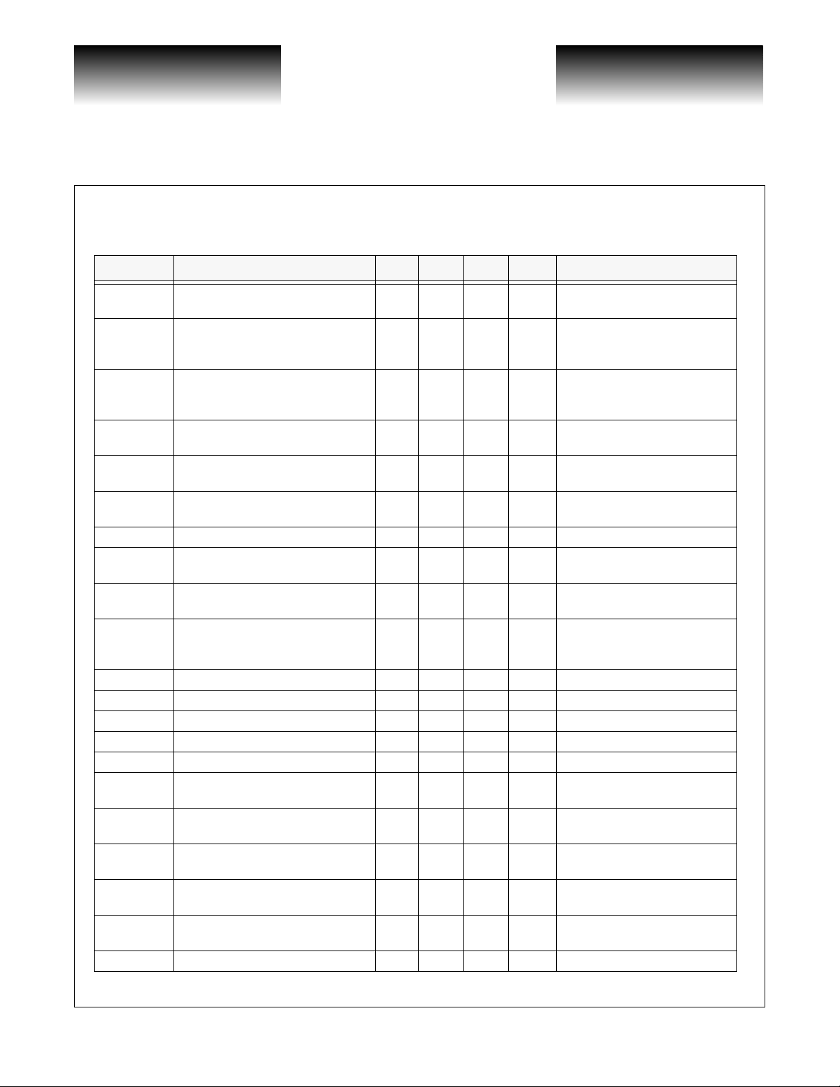
Electrical Characteristics
Table 1: AC Specifications
Symbol Parameter Min Typ Max Units Conditions
∆I
PH
I
PHS-AVG
I
PHS-PEAK
∆V
OUT-SE
∆V
OUT-DIFF
t
, t
R
F
(1)
Z
T
(1)
∆Z
T
BW Upper -3dB Bandwidth 2.2 2.5 3.0 GHz
F
L
Z
O
PSRR Power Supply Rejection Ratio TBD
I
NOISE
C
PD
SD
H
SD
A-OPEN
SD
D-OPEN
SD
A-SHORT
SD
D-SHORT
SD
HIGH
SD
LOW
Input Photocurrent Swing 2.2 mA
A verage Photocurrent Sensitivity 4 µA
Peak Input Photocurrent Sensitivity 8 µA
Single-Ended Ou tput Voltage
Amplitude
Differential Output Vo ltage Am plitude 400 500 600 mV
Rise and Fall Time 60 100 ps
Transimpedance Gain 20k 27k 40k Ω Differential measurement
Ripple in Passband Transimpedance 1 dB
Lower -3dB Cutoff Frequency 100 kHz
Output Impedance 50 Ω Single-ended
Input-Referred rms Noise Current 500 nA 30kHz to 2.5GHz
Photodetector Capacitance 0.4 0.6 0.8 pF Bias vo ltage on detector at 2.0V
Signal Detect Hysterisis 1 2 4 dB Electrical meas urement on SD pin
Signal Detect Assertion L evel 3 5 9 µA
Signal Detect Deasseration Level 1.0 2.2 3.0 µA
Signal Detect Asseration Level 6 10 18 µA
Signal Detect Deasseration Level 2.0 4.4 6.0 µA
Signal Detect HIGH Logic Level
Signal Detect LOW Logic Level 0.5 0.8 V
200 250 300 mV
V
CCS
- 0.3
Peak-to-peak AC current
amplitude
-23dBm average optical power
with a detector responsitivity of
0.8A/W.
-23dBm average optical power
with a detector responsitivity of
0.8A/W.
Single-ended peak-to-peak
measurement, I
Differential peak-to-peak
measurement, IIN >20µA.
At 2.2mAp-p input photocurrent
swing. 20% to 80%.
Modulation frequency between F
and BW
Referenced to 10MHz,
CPD = 0.6pF
Referenced to 10MHz, CPD =
0.6pF with no external
components
Average photocurrent with SD
open.
Average photocurrent with SD
open.
Average photocurrent with SD
shorted to ground.
Average photocurrent with SD
shorted to ground.
V
VSC7969
>20µA.
IN
L
Page 2 G52355-0, Rev 2.0
© VITESSE SEMICONDUCTOR CORPORATION • 741 Calle Plano • Camarillo, CA 93012
Tel: (800) VITESSE • FAX: (805) 987-5896 • Email: prodinfo@vitesse.com
Internet: www.vitesse.com
02/09/01
VITESSE
SEMICONDUCTOR CORPORATION
Advance Product Information
VSC7969
3.125Gb/s Integrat ed Transim p eda nce
and Limiting Amplifier with Signal Detect
Symbol Parameter Min Typ Max Units Conditions
MON
DC Duty Cycle -5 +5 %
IMON
RANGE
IMON
OFFSET
R
J
D
J
NOTES: (1) The transimpedance gain is defined as ZT = (∆V
standard deviation of the edge of th e pat t ern, multiply the standard deviation by 14 to achieve the to ta l random jitter. (3) +K28.5
- K28.5 (00111110101100000101).
Slope of Linear Anal og Photocurrent
Monitor vs Input Optical Power
Photocurren t Monitor Lin earity Range 5 200 µA
Photocurrent Monitor Offset 0 1 0 µA
Random Jitter
Deterministic Jitter
(2)
(3)
OUT - DIFF
0.8 µA/µW
TBD ps Peak-to-peak
TBD ps Peak-to-peak
)/∆IPH. (2) Usi ng 111110000 0 patter n at 2.5 Gb/s to measur e the
0Ω to 2kΩ to V
responsitivity of 0.8A/W
Table 2: DC Specifications
Symbol Parameter Min Typ Max Units Conditions
GND Negative Supply Rail 0 V
V
CCS
V
CCD
ICC Power Supply Current 65 75 mA 3.3V
V
OUT-CM
V
ANODE
V
CATHODE
V
CAT-EXT
V
APD
Positive Supply Rail for 3.3V Operation 3.0 3.3 3.6 V
Positive Supply Rail for 5V Operation 4.5 5.0 5.5 V
-
V
Common-Mode Voltage on Output Pins
Internal DC Bias Voltage on Detector
Anode Contact
Interal DC Bias Voltage on Detector
Cathode Contact
External DC Bias Voltage Permissable
on Detector Cathode Contact
External DC Bias Voltage for Use with
Avalanche Photodetector
0.8 0.9 1.0 V
V
CCS
0.15V
CCS
125mV
-
3.3 10 V
60 V
V
CCS
Applicable to VOUTP and
VOUTN pins at 50Ω load.
V
with a detector
CC
Absolute Maximum Ratings
Power Supply Voltage (V
Power Supply Voltage (V
) ......................................................................................................................... 3.6V
CCS
)........................................................................................................................ 5.5V
CCD
(1)
(at TA = +25°C, unless otherwise specified)
Junction Temperature Range........................................................................................................-40°C to +125°C
Storage Temperature Range .........................................................................................................-40°C to +125°C
Relative Ambient Humidity .................................................................................................................85%/+85°C
NOTE: (1) CAUTION: Stresses listed under “Absolute Maximum Ratings” may be applied to devices one at a time without caus-
ing permanent damage. Functionality at or above the values listed is not implied. Exposure to these values for extended
periods may affect device reliability.
Recommended Operating Conditions
Positive Voltage Supply (V
Positive Voltage Supply (V
Negative Voltage Rail (GND) ............................................................................................................................ 0V
Ambient Temperature Range (T
G52355-0, Rev 2.0 Page 3
02/09/01
© VITESSE SEMICONDUCTOR CORPORATION • 741 Calle Plano • Camarillo, CA 93012
)......................................................................................................................3.3V
CCS
)......................................................................................................................5.0V
CCD
(1)
)
..............................................................................................-40°C to +85°C
A
Tel: (800) VITESSE • FAX: (805) 987-5896 • Email: prodinfo@vitesse.com
Internet: www.vitesse.com
VITESSE
SEMICONDUCTOR CORPORATION
3.125Gb/s Integrated Transimpedance
and Limiting Amplifier with Signal Detect
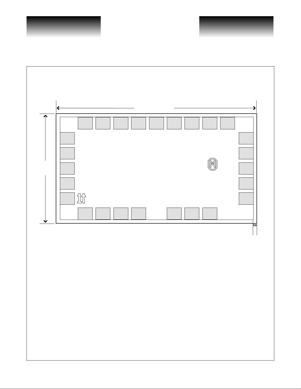
Bare Die Descriptions
Figure 1: Pad Assignments
1143µm
(45.0mil)
Pad 5
SD_ADJ
Pad 4
SD_TP
Pad 3
GND
Pad 2
BG_VREF
Pad 6
VOUTN
Pad 7
SD_OUT
Pad 8
GND
1467
Pad 9
VOUTN
VSC7969
µm (57.2mil)
Pad 10
GND
Advance Product Information
VSC7969
Pad 11
VOUTP
Pad 12
GND
Pad 13
IMON
Pad 14
VOUTP
Pad 15
GND
Pad 16
CSDN
Pad 17
CSDP
Pad 18
GND
Pad 1
GND
Pad 26
VCCD
Pad 25
VCCS
Pad 24
GND
Pad 23
IN
Die Size: 1143µm x 1453µm (45.0mil x 57.2mil)
Die Thickness: 279
µm (11.0mil)
Pad Size: 100µm x 100µm (3.9mil x 3.9mil)
Pad Passivation Opening: 86µm x 86µm (3.4mil x 3.4mil)
Scribe Size: 143µm (5.6mil)
Pad 22
FILTER
Pad 21
GND
Pad 20
GND
Pad 19
GND
143
µm
(5.6mil)
Page 4 G52355-0, Rev 2.0
© VITESSE SEMICONDUCTOR CORPORATION • 741 Calle Plano • Camarillo, CA 93012
Tel: (800) VITESSE • FAX: (805) 987-5896 • Email: prodinfo@vitesse.com
Internet: www.vitesse.com
02/09/01
VITESSE
SEMICONDUCTOR CORPORATION
Advance Product Information
VSC7969
3.125Gb/s Integrat ed Transim p eda nce
and Limiting Amplifier with Signal Detect
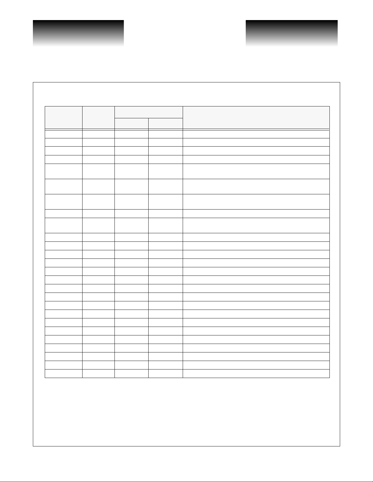
Table 3: Pad Coordinates
Signal
Name
GND 1 130 250 Negative power supply rail (typically 0V)
BG_VREF 2 130 375 Band Gap voltage reference 1.24V for testpoint, no connect
GND 3 130 500 Negative power supply rail (typically 0V)
SD_TP 4 130 625 Signal Detect test point, DO NOT CONNECT.
SD_ADJ 5 130 750
VOUTN 6 137 875
SD_OUT 7 280 875
GND 8 405 875 Negative power supply rail (typically 0V)
VOUTN 9 530 875
GND 10 655 875 Negative power supply rail (typ ically 0V)
VOUTP 11 780 875 Positive logic output (logic HIGH when photocurrent is HIGH)
GND 12 905 875 Negative power supply rail (typ ically 0V)
IMON 13 1030 875 Photocurrent Monitor
VOUTP 14 1173 875 Positive logic output (logic HIGH when photocurrent is HIGH)
GMD 15 1180 750 Negative power supply rail (typically 0V)
CSDN 16 1180 625 Test point for Signal Detect capacitor. DO NOT CONNECT.
CSDP 1 7 1180 500 Test point for Signal Detect capacitor. DO NOT CONNECT.
GND 18 1180 375 Negative power supply rail (typically 0V)
GND 19 1180 250 Negative power supply rail (typically 0V)
GND 20 1030 125 Negative power supply rail (typically 0V)
GND 21 905 125 Negative power supply rail (typ ically 0V)
FILTER 22 780 125 Photodetector cathode connection (filtered V
IN 23 530 125 Photodetector anode connection
GND 24 405 125 Negative power supply rail (typ ically 0V)
VCCS 25 280 125 Positive power supply rail for 3.3V operation
VCCD 26 137 125 Positive power supply rail for 5V operation
Pad
Number
Coordinates (µm)
X Y
Description
Signal Detect threshold adjustment (see Application am d Usage
section)
Complementary logic output (logi c LOW when photocurrent is
HIGH)
Signal detect output (logic HIGH when photocurrent exceeds
)
SD
A
Complementary logic output (logi c LOW when photocurrent is
HIGH)
)
CC
G52355-0, Rev 2.0 Page 5
02/09/01
© VITESSE SEMICONDUCTOR CORPORATION • 741 Calle Plano • Camarillo, CA 93012
Tel: (800) VITESSE • FAX: (805) 987-5896 • Email: prodinfo@vitesse.com
Internet: www.vitesse.com
 Loading...