

VITESSE VSC7962W, VSC7962RO Datasheet

VITESSE
SEMICONDUCTOR CORPORATION
Advance Product Information
VSC7962
3.125Gb/s PECL Limiting Amplifi er with LOS Detect
and Laser Driver with Automatic Powe r Control
G52361-0, Rev 2.1 Page 1
05/01/01
© VITESSE SEMICONDUCTOR CORPORATION • 741 Calle Plano • Camarillo, CA 93012
Tel: (800) VITESSE • FAX: (805) 987-5896 • Email: prodinfo@vitesse.com
Internet: www.vitesse.com
Features Applications
General Description
The VSC7962 is a single 3.3V supply combination limiting amplifier and laser diode driver for
SONET/SDH applications up to 3.125Gb/s. The limiting amplifier features Loss of Signal (LOS) detect, output
offset correction, and optional output squelch. Laser driver data inputs accept differential PECL signals and the
output modulation and bias currents are easily controlled via external components. The laser diode driver Automatic Power Control (APC) loop mai ntains a con sta nt average o ptical power o ver te mperature and l ife time. The
dominant pole of the APC loop can be controlled with an external capacitor. Other features include enable control, short-circuit protection for the modulation a nd bias inputs, short rise and fall times, and failure-mo nitor
output to indicate when the APC loop is unable to maintain the average optical power. The VSC7962 is available in die form or in a 48-pin TQFP package. The VSC7960 provides similar features to the VSC7962 but the
limiting amplifier has CML outputs.
Block Diagram
• 3.3V Power Supply
• Laser Driver AC-Coupled to Laser Diode
• Programmable Laser Driver Modulation Current
from 5mA to 60mA
• Programmable Laser Driver Bias Current from
1mA to 100mA
• Laser Driver Enable Control
• Automatic Optical Average Power Control
• Supply Current of 80mA
• PECL Limiting Amplifier Outputs
• 48-Pin TQFP Package
• SONET/SDH at 622Mb/s, 1.244Gb/s, 2.488Gb/s
and 3.125Gb/s
• Full-Speed Fibre Channel (1.062Gb/s)
VSC7939
VSC7961
Limiting Amplifier
Laser Driver
DA TA+
DA TA-
LAO+
LAO-
OUT+
OUT -
IN+ IN-
VSC7962
VITESSE
SEMICONDUCTOR CORPORATION
Advance Product Information
VSC7962
3.125Gb/s PECL Limiting Amplifier with LOS Detect
and Laser Driver with Automatic Power Control
Page 2 G52361-0, Rev 2.1
05/01/01
© VITESSE SEMICONDUCTOR CORPORATION • 741 Calle Plano • Camarillo, CA 93012
Tel: (800) VITESSE • FAX: (805) 987-5896 • Email: prodinfo@vitesse.com
Internet: www.vitesse.com
Electrical Characteristics
Table 1: Limiting Amplifier DC Specifications
NOTE: (1) See Figure5 for supply current measurement setup.
Table 2: Laser Driver DC Specifications
NOTES: (1) Both I
BIAS
and I
MOD
will turn off if any of the current set pins are grounded. (2) Assumes laser diode to monitor diode transfer
function does not change with temperature.
Symbol Parameter Min Typ Max Units Conditions
V
CC
Power Supply Range 3.135 5.5 V
I
CC
Power Supply Current
(1)
31 mA VCC = 3.3V
I
EE
Power Supply Current
(1)
38 mA VCC = 3.3V
I
CCSQ
Power Supply Current when Squelched
(1)
21 mA VCC = 3.3V
I
EESQ
Power Supply Current when Squelched
(1)
24 mA VCC = 3.3V
I
SQ
Squelch Input Curr en t 0 400 µA
PSSR Power Sup ply Rejection Ratio 20 30 dB f < 2MHz
Symbol Parameter Min Typ Max Units Conditions
V
CC
Power Supply Voltage Ran ge 3.125 3.465 V
I
CC
Supply Current TBD 45 mA
R
MODSET
=7.3kΩ,
R
BIASMAX
=4.8kΩ
I
BIAS
and I
MOD
excluded VCC=5V
I
BIAS
Bias Current Range 1 100 mA Voltage at BIAS pin=(VCC-1.6)
I
BIAS-OFF
Bias Off Current 100 µA ENABLE=low or DISABLE=high
(1)
S
BIAS
Bias Current Stability
230
ppm/°C
APC open loop. I
BIAS
=100mA
900 APC open loop. I
BIAS
=1mA
Bias Current Absolute Accuracy ±15 % Refers to part-to-part variation.
VR
MD
Monitor Diode Reve r se B ia s Vo lta g e 1.5 V
I
MD
Monitor Diode Reverse Current Range 18 1000 µA
Monitor Diode Bias Setpoint Stability
-480 50 480
ppm/°C
I
MD
=1mA
(1)
90 IMD=18µA
(1)
Monitor Diode Bias Absolute Accuracy -15 15 % Refers to part-to-part variation.
I
MOD
Modulation Current Range 5 60 mA
I
MOD-OFF
Modulation Off Current 200 µA ENABLE=low or DISABLE=high
(2)
Modulation Current Absolute Accuracy ±15 % See Note 2
Modulation Current Stability
-480 -50 480
ppm/°C
I
MOD
=60mA
250 I
MOD
=5mA
VITESSE
SEMICONDUCTOR CORPORATION
Advance Product Information
VSC7962
3.125Gb/s PECL Limiting Amplifi er with LOS Detect
and Laser Driver with Automatic Powe r Control
G52361-0, Rev 2.1 Page 3
05/01/01
© VITESSE SEMICONDUCTOR CORPORATION • 741 Calle Plano • Camarillo, CA 93012
Tel: (800) VITESSE • FAX: (805) 987-5896 • Email: prodinfo@vitesse.com
Internet: www.vitesse.com
Table 3: Limiting Amplifier AC Specifications
NOTES: (1) Deterministic Jitter measured peak-to-peak with K28.5 pattern. (2) Random Jitter measured with minimum input.
Table 4: Laser Driver AC Specifications
NOTES: (1) Measured with 622Mb /s 0- 1 pattern, LATCH=high. (2) PW D = (wider pulse - na rrower pul s e) / 2)
Symbol Parameter Min Typ Max Units Conditions
Data Rate 3.125 Gb/s
V
IN
Input Voltage Range 10 1200 mV peak-to-peak
J
D
Deterministic Jitter 25 ps See Note 1
J
R
Random Jitter 8 ps rms, see Note 2
t
R, tF
Rise/Fall Times 55 100 ps 20%-80%
v
N
Input Referred Noise 230 µV rms, IN+ to IN-
R
DIFF
Differential Input Resistance 100 W IN+ to IN-
f
L
Low Frequency Cut-of f
2MHzC
Z
open
2kHzC
Z
=0.1µF
V
SQ
Output Signal when Sq ue lc he d 20 mV Outputs AC-coupled
V
OH
PECL Output High Voltage
-1025 -850 mV
-850 mV Squelched
V
OL
PECL Output Low Voltage
-1810 -1620 mV
-1620 mV Squelched
Z
O
Output Resistance 100 Ω Single-ended
Symbol Parameter Min Typ Max Units Conditions
t
SU
Input Latch Setup Time 100 ps LATCH=high
t
H
Input Latch Hold Time 100 ps LATCH=high
Enable/Start-up Delay 250 ns
t
R
Output Rise Time 60 80 ps 20% to 80%
t
F
Output Fall Time 60 80 ps 20% to 80%
PWD Pulse Width Distortion 10 50 ps See Notes 1, 2
CID
MAX
Maximum Consecutive Identical Digits 80 bits
t
J
Jitter Generation 7 20 ps
p-p
Jitter BW=12kHz to 20MHz,
0-1 pattern.
VITESSE
SEMICONDUCTOR CORPORATION
Advance Product Information
VSC7962
3.125Gb/s PECL Limiting Amplifier with LOS Detect
and Laser Driver with Automatic Power Control
Page 4 G52361-0, Rev 2.1
05/01/01
© VITESSE SEMICONDUCTOR CORPORATION • 741 Calle Plano • Camarillo, CA 93012
Tel: (800) VITESSE • FAX: (805) 987-5896 • Email: prodinfo@vitesse.com
Internet: www.vitesse.com
Table 5: PECL and TTL/CMOS Inputs and Outputs Specifications
Table 6: Limiting Amplifier Loss of Signal Specifications
Table 7: Limiting Amplifier Loss of Signal Truth Table
Symbol Parameter Min Typ Max Units Conditions
V
ID
Differential Input Voltage 100 1600 mV
p-p
(DATA+) - (DATA-)
V
ICM
Common-Mode Input Voltage
V
CC
-
1.49
VCC -
1.32
VCC V
ID
/4
V PECL compatible
I
IN
Clock and Data Input Current -1 10 µA
V
IH
TTL Input High Voltage
(ENABLE, LATCH, DISABLE)
2.0 V
V
IL
TTL Input Low Voltage
(ENABLE, LATCH, DISABLE)
0.8 V
V
OH
TTL Output High Voltage (FAIL)2.4
V
CC
-
0.3
V
CC
V Sourcing 50µA
V
OL
TTL Output Low Voltage (FAIL) 0.1 0.44 V Sinking 100µA
Symbol Parameter Min Typ Max Units Conditions
H
LOS
LOS Hysteresis 3.1 3.3 5.5 dB H
LOS
= 20 log (V
THD
/ V
THA
)
t
LOS
LOS Assert / Deassert Time 0.22 0.25 0.28 µs
V
THA
LOS Assert Threshold
8.2
mV
R
TH
=2.5kΩ
12.8 19.8 21.8 R
TH
=7kΩ
57.2 RTH=20kΩ
V
THD
LOS Deassert Threshold
11.4
mV
R
TH
=2.5kΩ
26.2 29 31.6 R
TH
=7kΩ
75.2 RTH=20kΩ
V
LOSH
LOS Output High Voltage 3.3 V I
LOS
=-30µA
V
LOSL
LOS Output Low Voltage 0.168 V I
LOS
=+1.2µA
SQUELCH LOS Output
High High Off
Low High On
High Low On
Low Low On
VITESSE
SEMICONDUCTOR CORPORATION
Advance Product Information
VSC7962
3.125Gb/s PECL Limiting Amplifi er with LOS Detect
and Laser Driver with Automatic Powe r Control
G52361-0, Rev 2.1 Page 5
05/01/01
© VITESSE SEMICONDUCTOR CORPORATION • 741 Calle Plano • Camarillo, CA 93012
Tel: (800) VITESSE • FAX: (805) 987-5896 • Email: prodinfo@vitesse.com
Internet: www.vitesse.com
Absolute Maximum Ratings
(1)
Power Supply Voltage (VCC)...............................................................................................................-0.5V to 6V
Current into BIAS....................................................................................................................-20mA to +150mA
Current into OUT+, OUT- ..............................................................................................................................TBD
Current into MD ............................................................................................................................-5mA to +5mA
Current into FAIL
.........................................................................................................................-10mA to 30mA
Voltage at DATA+, DATA-, ENABLE, LATCH, FAIL
......................................................-0.5V to (VCC + 0.5V)
Voltage at MODSET, BIASMAX, APCSET_MD .........................................................................-0.5V to +3.0V
Voltage at BIAS..................................................................................................................-0.5V to (V
CC
+ 0.5V)
Voltage at OUT+, OUT-......................................................................................................-0.5V to (V
CC
+ 1.5V)
Continouous Power Dissipation (T
A
= +85°C, TQFP derate 20.8mW/°C above +85°C)....................... 1350mW
Operating Junction Temperature Range ......................................................................................-55°C to +150°C
Storage Temperature Range.........................................................................................................-55°C to +165°C
NOTE: (1) CAUTION: Stresses listed under “Absolute Maximum Ratings” may be applied to devices one at a time without caus-
ing permanent damage. Functionality at or above the values listed is not implied. Exposure to these values for extended
periods may affect device reliability.
Recommended Operating Conditions
Positive Voltage Rail (VCC)..........................................................................................................................+3.3V
Junction Temperature Range (T
J
)................................................................................................-40°C to +100°C
Ambient Temperature Range (T
A
).................................................................................................-40°C to +85°C
VITESSE
SEMICONDUCTOR CORPORATION
Advance Product Information
VSC7962
3.125Gb/s PECL Limiting Amplifier with LOS Detect
and Laser Driver with Automatic Power Control
Page 6 G52361-0, Rev 2.1
05/01/01
© VITESSE SEMICONDUCTOR CORPORATION • 741 Calle Plano • Camarillo, CA 93012
Tel: (800) VITESSE • FAX: (805) 987-5896 • Email: prodinfo@vitesse.com
Internet: www.vitesse.com
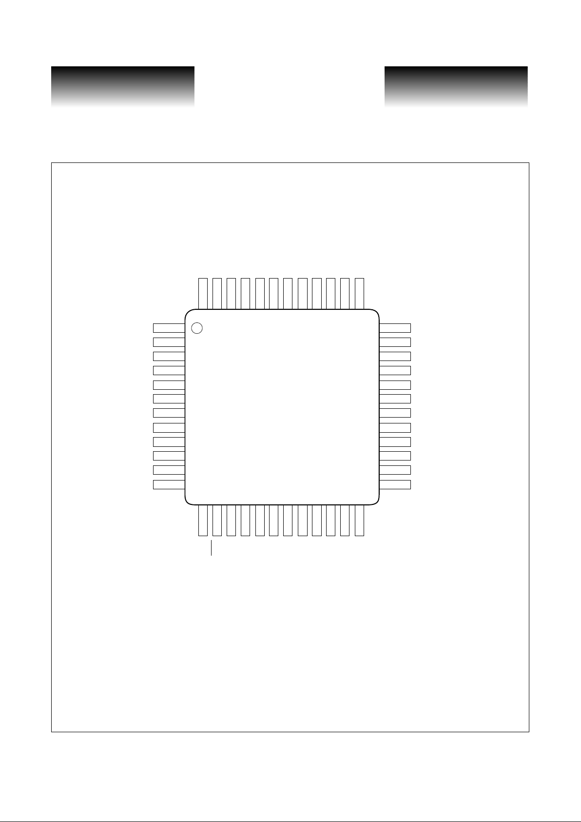
Package Pin Descriptions
Figure 1: Pin Diagram
1
2
3
4
5
6
7
8
9
10
11
12
GND
SQUELCH
VCCA
GND
CZ1
CZ2
GND
GND
IN+
IN-
GND
LEVEL
BIASMON
MODMON
GND
BIASMAX
MODSET
VCC
GND
RESERVED
APCSET_MD
CAPC
NC
ENABLE
13
14
15
16
17
18
19
20
21
22
23
24
TH
LOS
LOS
GND
GND
BIAS
VCC
OUT+
OUT-
VCC
GND
DISABLE
48
47
46
45
44
43
42
41
40
39
38
37
VCC
LAO+
LAO-
VCC
GND
VCC
GND
GND
VCC
DATA-
DATA+
VCC
36
35
34
33
32
31
30
29
28
27
26
25
VSC7962
VITESSE
SEMICONDUCTOR CORPORATION
Advance Product Information
VSC7962
3.125Gb/s PECL Limiting Amplifi er with LOS Detect
and Laser Driver with Automatic Powe r Control
G52361-0, Rev 2.1 Page 7
05/01/01
© VITESSE SEMICONDUCTOR CORPORATION • 741 Calle Plano • Camarillo, CA 93012
Tel: (800) VITESSE • FAX: (805) 987-5896 • Email: prodinfo@vitesse.com
Internet: www.vitesse.com
Table 8: Pin Description
Pin Name Pad Name
Pin/Pad
Number
Section Description
GND
GNDA or
GND
1, 4, 7, 8,
11, 16,
17, 23,
30, 34,
41, 42, 44
Both Ground
VCC VCC or VCCA
3, 19, 22,
31, 37,
40, 43,
45, 48
Both 3.3V Supply
SQUELCH SQ 2
Limiting
Amplifier
Squelch Input. Squelch is disabled if this pin in unconnected or
set low. When SQUELCH is high, OUT+ and OUT- are forced
to static levels. See Detailed Description section.
CZ1 CZ1 5
Limiting
Amplifier
Offset Correction Loop Capacitor. Place capacitor between this
pin and CZ2 to alter time con s ta nt of offset correction loop.
See Detailed Description section.
CZ2 CZ2 6
Limiting
Amplifier
Offset Correction Loop Capacitor. Place capacitor between this
pin and CZ1 to alter time con s ta nt of offset correction loop.
See Detailed Description section.
IN+ LAINP 9
Limiting
Amplifier
Noninverted Limiting Amplifier Input Signal
IN- LAINM 10
Limiting
Amplifier
Inverted Limiting Amplifier Input Signal
LEVEL LVL 12
Limiting
Amplifier
Output Current Level. This pin may be either connected to
GND or left unconnected. Connecting to GND causes output
current to be 20mA. The output is 1 6mA when unconnected.
See Detailed Description section.
TH TH 13
Limiting
Amplifier
Loss of Signal (LOS) Threshold. Connect a resistor from this
pin to GND to set the input signal level at which LOS outputs
will be asserted. See Applications Information section.
LOS
LOS 14
Limiting
Amplifier
Inverted Loss of Signal Output. LOS
is high for input signals
above the threshold programmed by TH. See Detailed
Description section.
LOS LOS 15
Limiting
Amplifier
Noninverted Loss-of -Signal Output. LOS i s low for input
signals above the thre shold programmed by TH. See Detailed
Description section.
BIAS BIAS 18
Laser
Driver
Laser Bias current output
OUT+ OUT+ 20
Laser
Driver
Noninverted Laser Modulation Current Output. I
MOD
flows
when input data is high.
OUT- OUT- 21
Laser
Driver
Inverted Laser Modulation Current Output. I
MOD
flows when
input data is low.
 Loading...