

VITESSE VSC7959W, VSC7959YD Datasheet
VITESSE
SEMICONDUCTOR CORPORATION
Advance Product Information
VSC7959
3.125Gb/s CML Limiting Amplifier with LOS Detect
Features Applications
• 3.3V or 5V Power Supply
• Typical Supply Current of 32mA
• Current-Mode Logic Outputs
• Optional Output Squelch
• Loss of Signal Detect
• Output Offset Correction
• Rise/Fall Times Faster than 100ps
• Packages: TSSOP-16, Bare Die
• SONET/SDH at 622Mb/s, 1.244Gb/s, 2.488Gb/s,
and 3.125Gb/s
• Full-Speed Fibre Channel (1.062Gb/s)
• Small Form Factor (SFF) Receivers
• ATM Optical Receivers
General Description
The VSC7959 is a single supply limiting amplifier with Loss of Signal (LOS) detect for SONET/SDH and
Fibre Channel applications up to 3.125Gb/s. The VSC7959 provides a constant output signal swing for a wide
range of input voltages a nd h as Current -Mode Logic ( CML) outp uts. Th e VSC796 1 pro vides the same funct ionality as the VSC7959 with positive emitter-coupled logic (PECL) outputs. Key features of the VSC7959 are its
RMS power detectors for programmable LOS detection, optional output squelch, adjustable output levels,
excellent jitter performance, and fast edge rates. The VSC7959 is available in die form or in a TSSOP-16 package.
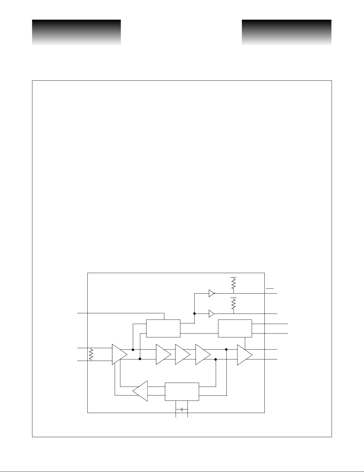
Block Diagram
VSC7959
TH
IN+
100
IN-
V
CC
8k
Ω
LOS
V
CC
8k
Ω
LOS
RMS Power
Detect and
Control
Ω
Lowpass Filter
Offset Correction
10pF
CZ1 CZ2
Output Control
SQUELCH
LEVEL
OUT+
OUT-
G52358-0, Rev 2.0 Page 1
02/09/01
© VITESSE SEMICONDUCTOR CORPORATION • 741 Calle Plano • Camarillo, CA 93012
Tel: (800) VITESSE • FAX: (805) 987-5896 • Email: prodinfo@vitesse.com
Internet: www.vitesse.com
VITESSE
SEMICONDUCTOR CORPORATION
Advance Product Information
3.125Gb/s CML Limiting Amplifier with LOS Detect
Electrical Characteristics
Table 1: DC Specifications
Symbol Parameter Min Typ Max Units Conditions
V
CC
I
CC
I
EE
I
CCSQ
I
EESQ
I
SQ
PSSR Power Supply Rejection Ratio 20 30 dB f < 2MHz
NOTE: (1) See Figure 5 for supply current measurement setup.
Table 2: DC Specifications
Power Supply Voltage 3.135 5.5 V
Power Supply Current
Power Supply Current
Power Supply Current when
Squelched
Power Supply Current when
Squelched
Squelch Input Current 0 400 µA
(1)
(1)
(1)
(1)
31 mA VCC = 3.3V
35 mA V
38 mA VCC = 3.3V
43 mΑ V
21 mA VCC = 3.3V
25 mA V
24 mA VCC = 3.3V
28 mA V
CC
CC
CC
CC
= 5V
= 5V
= 5V
= 5V
VSC7959
Symbol Parameter Min Typ Max Units Conditions
Data Rate 3.125 Gb/s
V
IN
J
D
J
R
t
R, tF
V
N
R
DIFF
f
L
V
SQ
V
CML
Z
O
NOTES: (1) Deterministic jitter measured peak-to-peak with K28.5 pattern. (2) Random jitter measured with minimum input.
Input V oltage Range 10 1200 mV Peak-to-peak
Deterministic Jitter 25 ps See Note 1
Random Jitter 8 ps See Note 2, RMS
Rise and Fall Times 55 100 ps 20% to 80%
Input Referred Noise 230 µV RMS, IN+ to INDifferential Input Resistance 100 Ω IN+ to IN-
Low Frequency Cutof f
Output Signal When Squelched 20 mV Output AC-coupled
550 1200 mV Level = open, RL = 50Ω
CML Output Voltage
Output Resistance 100 Ω Single-ended
1100 1800 mV Level = GND, RL = 75Ω
2MHzC
2kHzC
20 mV Squelched
open
Z
= 0.1µF
Z
Page 2 G52358-0, Rev 2.0
© VITESSE SEMICONDUCTOR CORPORATION • 741 Calle Plano • Camarillo, CA 93012
Tel: (800) VITESSE • FAX: (805) 987-5896 • Email: prodinfo@vitesse.com
Internet: www.vitesse.com
02/09/01
VITESSE
SEMICONDUCTOR CORPORATION
Advance Product Information
VSC7959
3.125Gb/s CML Limiting Amplifier with LOS Detect
Table 3: Loss of Signal Specifications
Symbol Parameter Min Typ Max Units Conditions
H
I
V
V
V
V
LOS
LOS
THA
THD
LOSH
LOSL
LOS Hystersis 3.1 3.3 5.5 dB H
LOS Assert/Deassert Time 0.22 0.25 0.28 µs
8.2 mV R
LOS Assert Threshold
LOS Deassert Threshold
LOS Output HIGH Volta ge 3.3 V I
LOS Output LOW Voltage 0.168 V I
12.8 19.8 21.8 mV R
57.2 mV R
11.4 mV R
26.2 29.0 31.6 mV R
75.2 mV R
= 20 log (V
LOS
= 2.5kΩ
TH
= 7kΩ
TH
= 20kΩ
TH
= 2.5kΩ
TH
= 7kΩ
TH
= 20kΩ
TH
= –30µA
LOS
= +1.2µA
LOS
Table 4: Loss of Signal Truth Table
SQUELCH LOS Output
High Low Off
Low High On
High Low On
Low Low On
THD/VTHA
)
Absolute Maximum Ratings
(1)
Power Supply Voltage (VCC).............................................................................................................-0.5V to +6V
Maximum Junction Temperature Range .........................................................................................................TBD
Storage Temperature Range (T
NOTE: (1) CAUTION: Stresses listed under “Absolute Maximum Ratings” may be applied to devices one at a time without caus-
ing permanent damage. Functionality at or above the values listed is not implied. Exposure to these values for extended
periods may affect device reliability.
).................................................................................................-55°C to +150°C
S
Recommended Operating Conditions
Positive Voltage Rail (VCC)..................................................................................................................3.3V or 5V
Junction Temperature Range (T
Ambient Temperature Range (T
G52358-0, Rev 2.0 Page 3
02/09/01
© VITESSE SEMICONDUCTOR CORPORATION • 741 Calle Plano • Camarillo, CA 93012
)................................................................................................-40°C to +100°C
J
).................................................................................................-40°C to +85°C
A
Tel: (800) VITESSE • FAX: (805) 987-5896 • Email: prodinfo@vitesse.com
Internet: www.vitesse.com
 Loading...