

VITESSE VSC7958X, VSC7958CC Datasheet
VITESSE
SEMICONDUCTOR CORPORATION
Preliminary Data Sheet
VSC7958
2.5Gb/s High Speed Limiting Post Amplifier
for OC-48/SDH-16 Applications
Features
• 2.5Gb/s Data Rates (OC-48/SDH-16)
• Input Offset Error Cancellation
• Single 5V Power Supply
• Fully Differential Architecture
General Description
The Vitesse high speed limiting amplifier is intended for use as a post amplifier in wide band fiber optic
links with data rates up to 2.5 Gb/s. Thi s amplifi er provi des ver y high sensit ivity an d broadband op erat ion wit h a
fully differential architecture. Additional features include on-chip, offset-correction circuitry to provide excellent pulse width distortion characteristics.
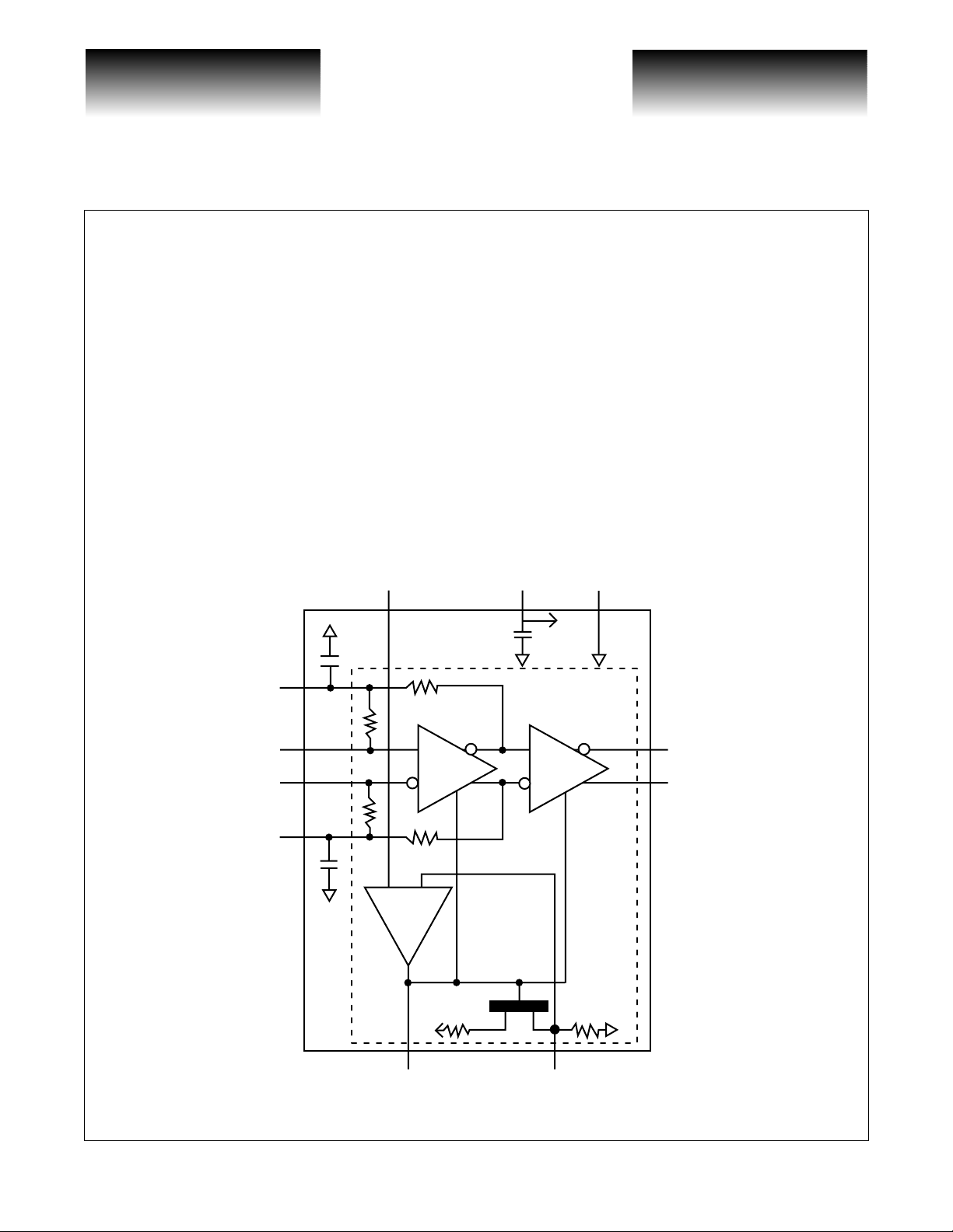
VSC7958 Block Diagram
VBR
VSS GND
VREF-
VIN-
VIN+
VREF+
50
50
Chip Boundary
A1 A2
+-
VBF VBS
VOUTVOUT+
G52184-0, Rev 3.0 Page 1
05/14/01
© VITESSE SEMICONDUCTOR CORPORATION • 741 Calle Plano • Camarillo, CA 93012
Tel: (800) VITESSE • FAX: (805) 987-5896 • Email: prodinfo@vitesse.com
Internet: www.vitesse.com
VITESSE
SEMICONDUCTOR CORPORATION
2.5Gb/s High Speed Limiting Post Amplifier
Preliminary Data Sheet
for OC-48/SDH-16 Applications
T able 1: Electrical Specifications
All min and max values are tested at VSS = -4.5V and -5.5V, unless otherwise noted. All min and max values are guaranteed from
T
= 0°C to 85°C, unless otherwise noted.
CASE
Symbol Parameter Min Typ Max Units Conditions
(1)
VIN±
+) - (VIN-)
(V
IN
+) - (V
(V
REF
(V
+) - (V
OUT
V
OFFSET
PW% Output Pulse Width 90 100 110 %
, t
t
R
F
G Small Signal Gain 26 30 45 dB
(1)
f
MAX
(1)
f
MIN
(1)
S
11
(1)
S
22
I
SS
(1)
NF
(1)
V
NR
θ
JC
NOTE:(1) These values are not measured during production test. These values are results of engineering characterization.
Input Voltage Swing - - 800 mV
(1)
Input Voltage Swing - - 1600 mV
-) Input Offset Voltage Swing - 10 25 mV VIN = 0
REF
Single-ended source
p-p
Differential source
p-p
Differential Output Swing.
-) Output Voltage Swing 320 500 1200 mV
OUT
p-p
V
IN
Input peak-to -peak
Output DC Offset Voltage - -0.5 - V Measured to ground
Rise and Fall Time - 100 - ps
20%-80%, 25°C,
V
IN
V
IN
ended
Small Signal -3dB Bandwidth - 3 - GHz 25°C, VIN = 4mV
Low Frequency -3dB Cutoff - 30 - kHz 25°C, VIN = 4mV
Input Return Loss Reference to 50Ω - 15 - dB At 1. 5GHz
Output Return Loss Reference to 50Ω - 15 - dB At 1.5 GHz
Supply Current - 80 100 mA
Noise Figure - 15 - dB 8kHz to 18GHz
Total single-ended output
Input Referred Wide Band Noise - 170 - µV
noise voltage divided by
rms
small-signal gain. 8kHz to
18GHz
Thermal Resistance - 30 - °C/W Junction-to-case
= 8mV, Differential
= 50mV
= 4mV
VSC7958
single-
p-p
p-p
p-p
Page 2 G52184-0, Rev 3.0
© VITESSE SEMICONDUCTOR CORPORATION • 741 Ca l le Pl an o • Camarillo, CA 93012
Tel: (800) VITESSE • FAX: (805) 987-5896 • Email: prodinfo@vitesse.com
Internet: www.vitesse.com
05/14/01
VITESSE
SEMICONDUCTOR CORPORATION
Preliminary Data Sheet
VSC7958
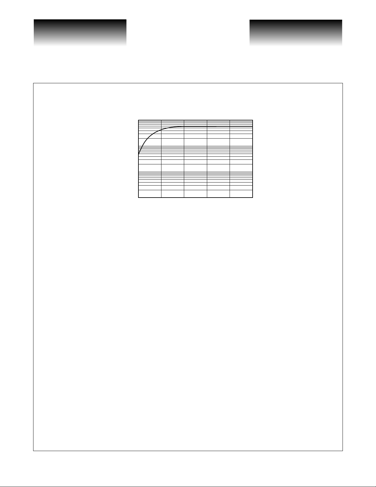
Figure 1: Typical Output Voltage vs. Input Voltage of Limiting Amplifier
1000
100
10
Single-Ended Output Voltage (mV)
Absolute Maximum Ratings
Output Voltage vs. Input Voltage
1
1
13
Single-Ended Input Voltage (mV)
(1)
(at TA = 25°C unless otherwise specified)
2.5Gb/s High Speed Limiting Post Amplifier
for OC-48/SDH-16 Applications
20 100 260 500
Power Supply Voltage (VSS) ...............................................................................................................-7V to -0.5V
Power Dissipation.............................................................................................................................................. 1W
All Pins............................................... ........ .........................................................................................V
SS
(VREF+) - (VIN+): ..........................................................................................................................................±2V
(VREF-) - (VIN-): ........................................................................................................................................... ±2V
Storage Temperature Range (T
)................................................................................................ -40°C to 125°C
STG
Operating Temperature Range ............................................................................................................0°C to 100°C
NOTE: (1) CAUTION: Stresses listed under “Absolute Maximum Ratings” may be applied to devices one at a time without caus-
ing permanent damage. Functionality at or above the values listed is not implied. Exposure to these values for extended
periods may affect device reliability.
to + .5V
Recommended Operating Conditions
Case Temperature Range (TC)..............................................................................................................0°C to 85°C
Negative Voltage Rail (V
Bit Rate = 2.488Gb/s NRZ and data pattern = 2
G52184-0, Rev 3.0 Page 3
05/14/01
).............................................................................................................-5.5V to -4.7V
SS
© VITESSE SEMICONDUCTOR CORPORATION • 741 Calle Plano • Camarillo, CA 93012
Tel: (800) VITESSE • FAX: (805) 987-5896 • Email: prodinfo@vitesse.com
23
-1 PRBS, unless otherwise specified.
Internet: www.vitesse.com
 Loading...