

VITESSE VSC7939W, VSC7939RP Datasheet
VITESSE
SEMICONDUCTOR CORPORATION
Preliminary Data Sheet
VSC7939
Laser Diode Driver with Automatic Power Control
SONET/SDH 3.125Gb/s
Features Applications
• Power Supply: 3.3V or 5V ±5%
• AC-Coupled to Laser Diode
• Programmable Modulation Current: 5mA to 60mA
• Programmable Bias Current: 1mA to 100mA
• Enable /Disable Control
• Typical Rise/Fall Times of 60ps
• Automatic Optical Average Power Control
• Supply Current of 33mA at 3.3V
• SONET/SDH at 622Mb/s, 1.244Gb/s,
2.488Gb/s, 3.125Gb/s
• Full-Speed Fibre Channel (1.062Gb/s)
General Description
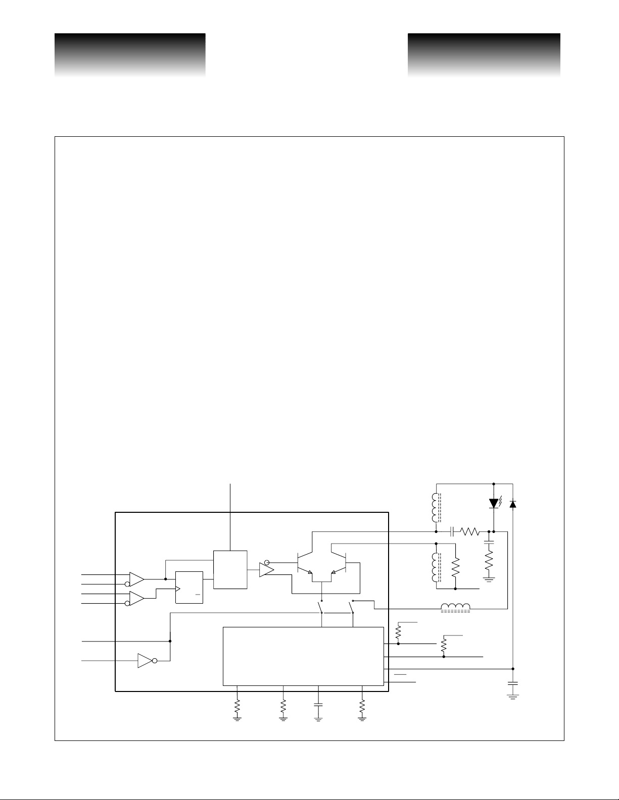
The VSC7939 is a single 3.3V or 5V supply l aser diode driv er special ly desig ned for S ONET/SDH appli cations up to 3.125Gb/s. External resistors set a wide range of bias and modulation currents for driving the laser.
Data and clock inputs accept differential PECL signals. The autom atic power control (APC) loop maintains a
constant average optical power over temperature and lifetime. The dominant pole of the APC loop can be controlled with an external capacitor. Other features include enable/disable control, short-circuit protection for the
modulation and bias inputs, short rise and fall times, programmable slow-start circuit to set laser turn-on delay,
and failure-monitor output to indicate when the APC loop is unable to maintain the average optical power. The
VSC7939 is available in die form or in a 32-pin TQFP package.
Block Diagram
V
P
L
C
D
P
L
V
CC
BIASMON
CC
C
F
R
F
V
CC
1nF
3.3V Operation
LATCH
IOUT+
IOUT-
MUX
DATA+
DATA-
CLK+
CLK-
ENABLE
DISABLE
G52350-0, Rev 3.2 Page 1
02/26/01
SET
D
Q
Q
CLR
APC
MODSET
© VITESSE SEMICONDUCTOR CORPORATION • 741 Calle Plano • Camarillo, CA 93012
Tel: (800) VITESSE • FAX: (805) 987-5896 • Email: prodinfo@vitesse.com
BIASMAX
Internet: www.vitesse.com
CAPC
APCSET
V
MODMON
MD
FAIL
BIAS
CC
VITESSE
SEMICONDUCTOR CORPORATION
SONET/SDH 3.125Gb/s
Preliminary Data Sheet
Laser Diode Driver with Automatic Power Control
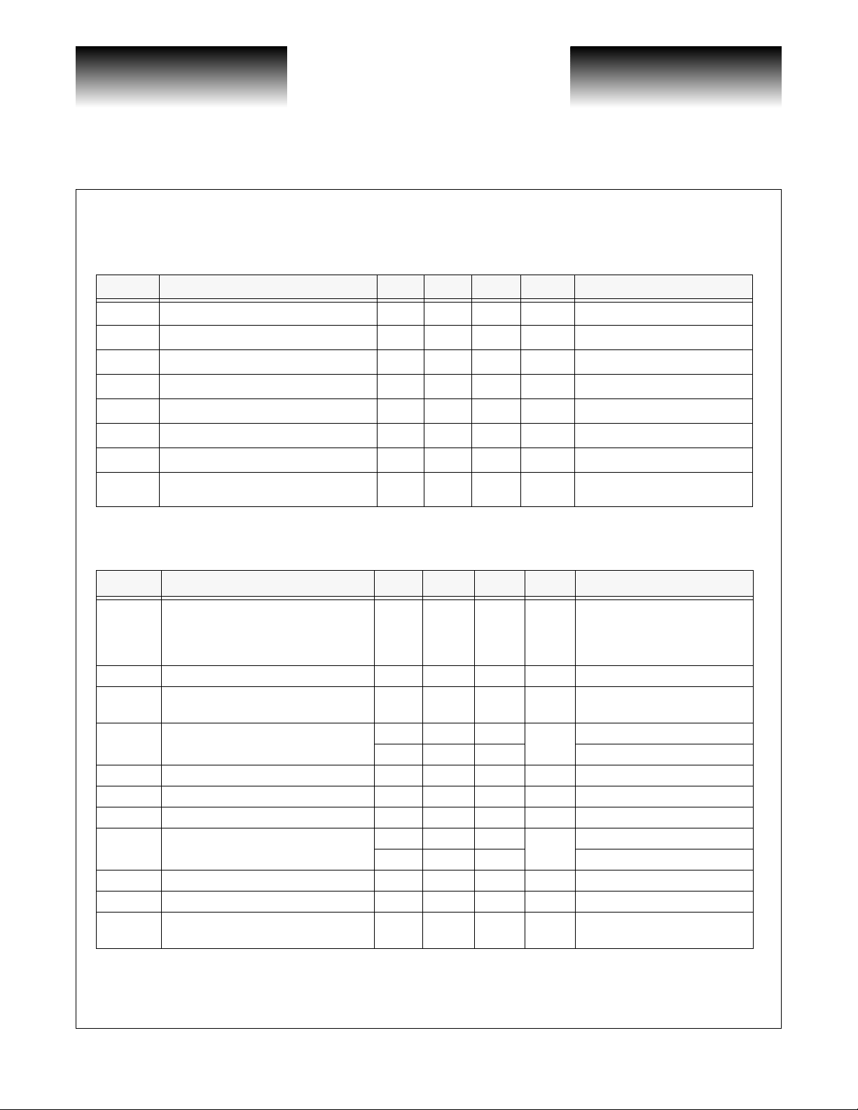
Electrical Characteristics
Table 1: AC Specifications
AC specifications are guaranteed by design an d characterization. Typical values are for 3.3V.
Symbol Parameter Min Typ Max Units Conditions
t
SU
t
H
t
R
t
F
PWD Pulse Width Distortion 10 50 ps See Notes 1, 2
CID
t
J
NOTES: (1) Measured with 622Mb/s 0-1 pattern , LATCH=high. (2) P WD = (wi der pulse - narrower pulse) / 2).
Input Latch Setup Time 100 ps LATCH=high
Input Latch Hold Time 100 ps LATCH=high
Enable/Start-up Delay 250 ns
Output Rise Time 60 80 ps 20% to 80%
Output Fall Time 60 80 ps 20% to 80%
Maximum Consecu tive Identical D igits 80 bits
MAX
Jitter Generation 7 20 ps
p-p
Jitter BW=12kHz to 20MHz,
0-1 pattern.
VSC7939
Table 2: DC Specifications
Symbol Parameter Min Typ Max Units Conditions
I
CC
I
BIAS
I
BIAS-OFF
S
BIAS
VR
MD
I
MD
I
MOD
I
MOD-OFF
R
Supply Current TBD 45 mA
Bias Current Range 1 100 mA Voltage at BIAS pin=(VCC-1.6)
Bias Off Current 100 µA
Bias Current Stability
Bias Current Absolute Accuracy ±15 % Refers to part-to-part variation
Monitor Diode Reverse Bias Voltage 1.5 V
Monitor Diode Reverse Current Range 18 1000 µA
Monitor Diode Bias Setpoint Stability
Monitor Diode Bias Absolute Accuracy -15 15 % Refers to part-to-part variation
Modulation Curren t Rang e 5 60 mA
Modulation Off Cu rr ent 200 µA
-480 -50 480
230
900 APC open loop. I
90 IMD=18µA
ppm/°C
ppm/°C
R
I
BIAS
V
ENABLE=low or
DISABLE=high
APC open loop. I
I
MD
ENABLE=low or
DISABLE=high
MODSET
BIASMAX
and I
=5V
CC
=1mA
=7.3kΩ
=4.8kΩ
MOD
(2)
(2)
excluded
(1)
BIAS
BIAS
(1)
=100mA
=1mA
Page 2 G52350-0, Rev 3.2
© VITESSE SEMICONDUCTOR CORPORATION • 741 Calle Plano • Camarillo, CA 93012
Tel: (800) VITESSE • FAX: (805) 987-5896 • Email: prodinfo@vitesse.com
Internet: www.vitesse.com
02/26/01

VITESSE
SEMICONDUCTOR CORPORATION
Preliminary Data Sheet
VSC7939
Laser Diode Driver with Automatic Power Control
SONET/SDH 3.125Gb/s
Symbol Parameter Min Typ Max Units Conditions
Modulation Current Absolute Accuracy ±15 % See Note 2
Modulation Current Stability
A
BIAS
A
MOD
NOTES: (1) Both I
BIASMON to I
MODMON to I
tion does not change with temperature.
BIAS
and I
-480 -50 480
250 I
Gain 37 A/A I
BIAS
Gain 29 A/A I
MON
will turn off if any of the current set pins are grounded. (2) Assume s l ase r di ode t o monitor diode transfer func-
MOD
ppm/°C
I
=60mA
MOD
=5mA
MOD
BIAS/IBIASMON
MOD/IMODMON
Table 3: PECL and TTL/CMOS Inputs and Outputs Specifications
Symbol Parameter Min Typ Max Units Conditions
V
ID
V
ICM
I
IN
V
IH
V
IL
Differential Input Voltage 100 1600 mV
-
V
Common-Mode Input V oltage
Clock and Data Input Current -1 10 µA
TTL Input High Voltage
(ENABLE, LATCH)
TTL Input Low Voltage
(ENABLE, LATCH)
TTL Output High Voltage (FAIL
TTL Output Low Vo ltage (FAIL
)2.4
) 0.1 0.44 V Sinking 100µA
CC
1.49
2.0 V
VCC -
1.32
V
0.3
CC
-
VCC V
/4
ID
0.8 V
V
CC
V PECL-compatible
V Sourcin g 50µA
(DATA+)-(DATA-)
p-p
G52350-0, Rev 3.2 Page 3
02/26/01
© VITESSE SEMICONDUCTOR CORPORATION • 741 Calle Plano • Camarillo, CA 93012
Tel: (800) VITESSE • FAX: (805) 987-5896 • Email: prodinfo@vitesse.com
Internet: www.vitesse.com

VITESSE
SEMICONDUCTOR CORPORATION
SONET/SDH 3.125Gb/s
Laser Diode Driver with Automatic Power Control
Absolute Maximum Ratings
Power Supply Voltage (VCC).............................................................................................................-0.5V to +7V
Current into BIAS.....................................................................................................................-20mA to +150mA
Current into OUT+, OUT-...............................................................................................................................TBD
Current into MD.............................................................................................................................-5mA to +5mA
Current into FAIL
Voltage at DATA+, DATA-, CLK+, CLK-, ENABLE, LATCH.........................................-0.5V to (V
Voltage at APCFILT, MODSET, BIASMAX, APCSET, MD, FAIL
Voltage at OUT+, OUT-..................................................................................................... -0.5V to (V
Voltage at BIAS..................................................................................................................-0.5V to (V
Continouous Power Dissipation (T
Operating Junction Temperature Range...................................................................................... -55°C to +150°C
Storage Temperature Range ........................................................................................................ -65 °C to +165°C
NOTE: (1) CAUTION: Stresses listed under “Absolute Maximum Ratings” may be applied to devices one at a time without caus-
ing permanent damage. Functionality at or above the values listed is not implied. Exposure to these values for extended
periods may affect device reliability.
......................................................................................................................... -10mA to 30mA
= +85°C, TQFP derate 20.8mW/°C above +85°C) .......................1350mW
A
(1)
.............................................-0.5V to +3.0V
Preliminary Data Sheet
VSC7939
CC
CC
CC
+ 0.5V)
+ 1.5V)
+ 0.5V)
Recommended Operating Conditions
Positive Voltage Rail (VCC).....................................................................................................+3.135V to +5.25V
Negative Voltage Rail (GND) ............................................................................................................................0V
Modulation Current (I
Ambient Temperature Range (T
NOTE: (1) VCC = 3.3V, I
MOD
BIAS
(1)
)
.......................................................................................................................30mA
).................................................................................................-40°C to +85°C
A
= 60mA.
Page 4 G52350-0, Rev 3.2
© VITESSE SEMICONDUCTOR CORPORATION • 741 Calle Plano • Camarillo, CA 93012
Tel: (800) VITESSE • FAX: (805) 987-5896 • Email: prodinfo@vitesse.com
Internet: www.vitesse.com
02/26/01
VITESSE
SEMICONDUCTOR CORPORATION
Preliminary Data Sheet
VSC7939
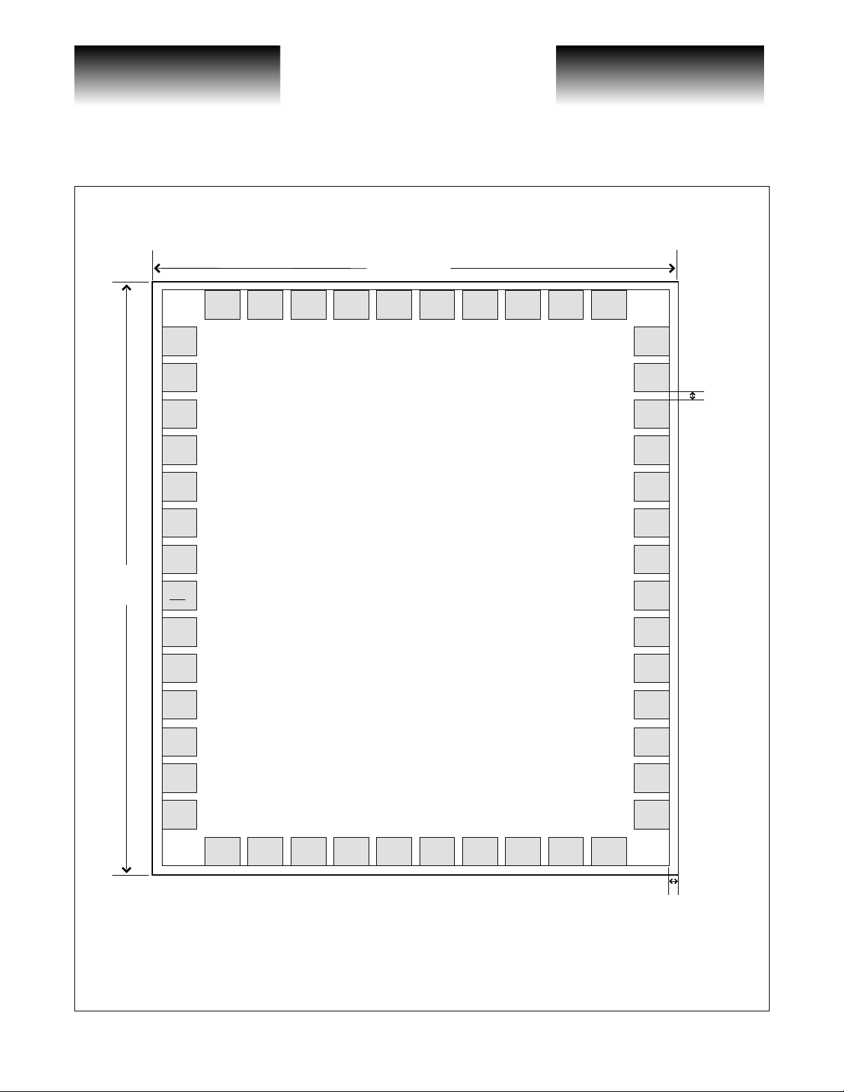
Bare Die Pad Descriptions
Pad 10
Pad 12
GND1
Pad 13
LATCH
Pad 14
ENABLE
Pad 15
DISABLE
Pad 16
GND1
Pad 17
BIASMON
Pad 11
VCC1
(Pin 7)
(Pin 8)
(Pin 9)
(Pin 10)
(Pin 11)
CLK-
Laser Diode Driver with Automatic Power Control
Figure 1: Pad Assignments
1773
µm (0.0698")
Pad 9
CLK+
Pad 8
VCC1
Pad 7
GND1
Pad 6
VCC1
Pad 5
DATA-
Pad 4
DATA+
SONET/SDH 3.125Gb/s
Pad 3
VCC1
(Pin 1)(Pin 2)(Pin 3)(Pin 4)(Pin 5)(Pin 6)
Pad 2
GND1
(Pin 32)
(Pin 31)
(Pin 30)
(Pin 29)
Pad 1
GND2
Pad 48
VCC2
Pad 47
BIASMAX
Pad 46
MODSET
Pad 45
GND2
Pad 44
APCSET
20
µm
(0.0008")
2233
µm
(0.0879")
Pad 18
(Pin 12)
MODMON
Pad 19
FAIL
Pad 20
GND4
Pad 21
PB_GND
Pad 22
APCFILT
Pad 23
GND4
Pad 24
VCC4
Pad 25
BIAS
(Pin 13)
(Pin 14)
(Pin 15)
(Pin 16)
(Pin 17)
Pad 26
PB_GND1
(Pin 18) (Pin 19) (Pin 20) (Pin 21) (Pin 22) (Pin 23) (Pin 24)
Pad 27
VCC4
Pad 28
DB_OUT+
Pad 29
OUT+
VSC7939
Pad 30
OUT-
Pad 31
DB_OUT-
Die Size: 1773µm x 2233µm (0.0698" x 0.0879")
Die Thickness: 625
µm (0.0246")
Pad Pitch: 115µm (0.0045")
Pad Size: 95µm x 95µm (0.0037" x 0.0037")
Pad to Pad Clearance: 20µm (0.0008
")
Pad Passivation Opening: 95µm x 95µm (0.0037" x 0.0037")
Scribe Size: 75µm (0.0030")
Pad 32
VCC4
Pad 33
GND4
Pad 34
GND3
(Pin 28)
(Pin 27)
(Pin 26)
(Pin 25)
Pad 35
MD
Pad 43
RESERVED
Pad 42
GND3
Pad 41
PB_GND
Pad 40
GND3
Pad 39
PB_GND
Pad 38
CAPC
Pad 37
VCC3
Pad 36
GND3
75
(0.0030")
µm
G52350-0, Rev 3.2 Page 5
02/26/01
© VITESSE SEMICONDUCTOR CORPORATION • 741 Calle Plano • Camarillo, CA 93012
Tel: (800) VITESSE • FAX: (805) 987-5896 • Email: prodinfo@vitesse.com
Internet: www.vitesse.com
VITESSE
SEMICONDUCTOR CORPORATION
SONET/SDH 3.125Gb/s
Laser Diode Driver with Automatic Power Control
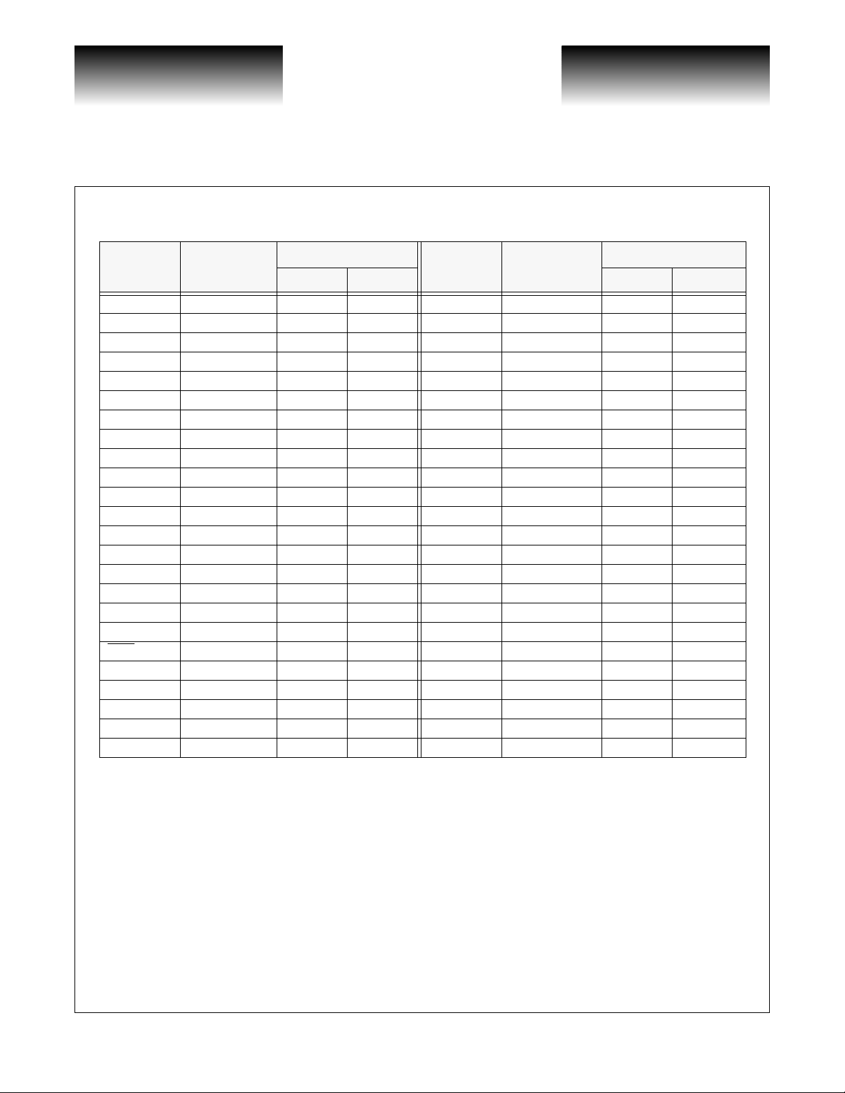
Table 4: Pad Coordinates
Signal
Name
GND2 1 1613.55 1863.475 BIAS 25 (Pin 17) 159.45 368.475
GND1 2 1414.525 2073.55 PB_GND 26 369.525 159.45
VCC1 3 (Pin 1) 1289.525 2073.55 VCC4 27 (Pin 18) 484.525 159.45
DATA+ 4 (Pin 2) 1174.525 2073.55 DB_OUT+ 28 599.525 159.45
DATA- 5 (Pin 3) 1059.525 2073.55 OUT+ 29 (Pin 19 ) 714.525 159.45
VCC1 6 (Pin 4) 944.525 2073.55 OUT– 30 (Pin 20) 829.525 159.45
GND1 7 829.525 2073.55 DB_OUT– 31 944.525 159.45
VCC1 8 714.525 2073.55 VCC4 32 (Pin 21) 1059.525 159.45
CLK+ 9 (Pin 5) 599.525 2073.55 GND4 33 (Pin 22) 1174.525 159.45
CLK- 10 (Pin 6) 484.525 2073.55 GND3 34 (Pin 23) 1289.525 159.45
VCC1 11 (Pin 7) 369.525 2073.55 MD 35 (Pin 24) 1404.525 159.45
GND1 12 159.45 1863.475 GND3 36 1613.55 368.475
LATCH 13 (Pin 8) 159.45 1748.475 VCC3 37 (Pin 25) 1613.55 483.475
ENABLE 14 (Pin 9) 159.45 1633.475 CAPC 38 (Pin 26 ) 1613.55 598.475
DISABLE 15 (Pin 10) 159.45 1518.475 PB_GND 39 1613.55 713 .475
GND 16 159.45 1403.4 GND3 40 (Pin 27) 1613.55 828.475
BIASMON 17 ( Pin 11) 159.45 1288.475 PB_GND 41 1613.55 943.475
MODMON 18 (Pin 12) 159.45 1058.475 GND3 42 1613.55 1058.475
FAIL
GND4 20 159.45 943.475 APCSET 44 (Pin 29) 1613.55 1288.475
PB_GND 21 159.45 828.475 GND2 45 1613.55 1403.475
APCFILT 22 (Pin 14) 159.45 713.475 MODSET 46 (Pin 30) 1613.55 1518.475
GND4 23 (Pin 15) 159.45 598.475 BIASMAX 47 (Pin 31) 1613.55 1633.475
VCC4 24 (Pin 16) 159.45 483.475 VCC2 48 (Pin 32) 1613.55 1748.475
Pad
No.
19 (Pin 13) 159.45 1058.475 RESERVED 43 (Pin 28) 1613.55 1173.475
Coordinates (µm)
X Y X Y
Signal
Name
Preliminary Data Sheet
VSC7939
Pad
No.
Coordinates (µm)
Page 6 G52350-0, Rev 3.2
© VITESSE SEMICONDUCTOR CORPORATION • 741 Calle Plano • Camarillo, CA 93012
Tel: (800) VITESSE • FAX: (805) 987-5896 • Email: prodinfo@vitesse.com
Internet: www.vitesse.com
02/26/01
 Loading...