

VITESSE VSC7934 Datasheet

VITESSE
SEMICONDUCTOR CORPORATION
Target Specification
VSC7934
Single Supply 2.5 Gb/s
Voltage Driver
G52181-0, Rev 1.1
VITESSE SEMICONDUCTOR CORPORATION
Page 1
10/14/97 741 Calle Plano, Camarillo, CA 93012 • 805/388-3700 • FAX: 805/987-5896
Features
Introduction
The VSC7934 is a single 5V supply, 2.5Gb/s voltage driver with direct access to the output modulation and
bias FET’s. The output stage can drive 60 mA into 50 Ohms with adequate output voltage compliance. Output
bias and modulation currents are set by external components allowing precision monitoring and setting of the
voltage levels.
Applications
• SONET OC12, OC24, OC48, SDH16
• Full Speed Fibre Channel (1.062 Gb/s)
VSC7934 Block Diagram
• Rise Times Typically 100ps
• High Speed Operation
(Up to 2.5 Gb/s NRZ Data)
• 3 Volt Output Voltage Compliance
• Single-ended or Differential Input Operation
• Single Power Supply, 5 Volt or 5.2 Volts
• Direct Access to Modulation and Bias FET’s
DIN
VREF
IBIAS1
OUTNOUT
VIP
VIB2
VIB1
MIP
MIB1
MIB2
IMOD
IBIAS2
I
NOUT
VITESSE
SEMICONDUCTOR CORPORATION
Target Specification
VSC7934
Single Supply 2.5 Gb/s
Voltage Driver
Page 2
VITESSE SEMICONDUCTOR CORPORATION
G52181-0, Rev 1.1
741 Calle Plano, Camarillo, CA 93012 • 805/388-3700 • FAX: 805/987-5896 10/14/97
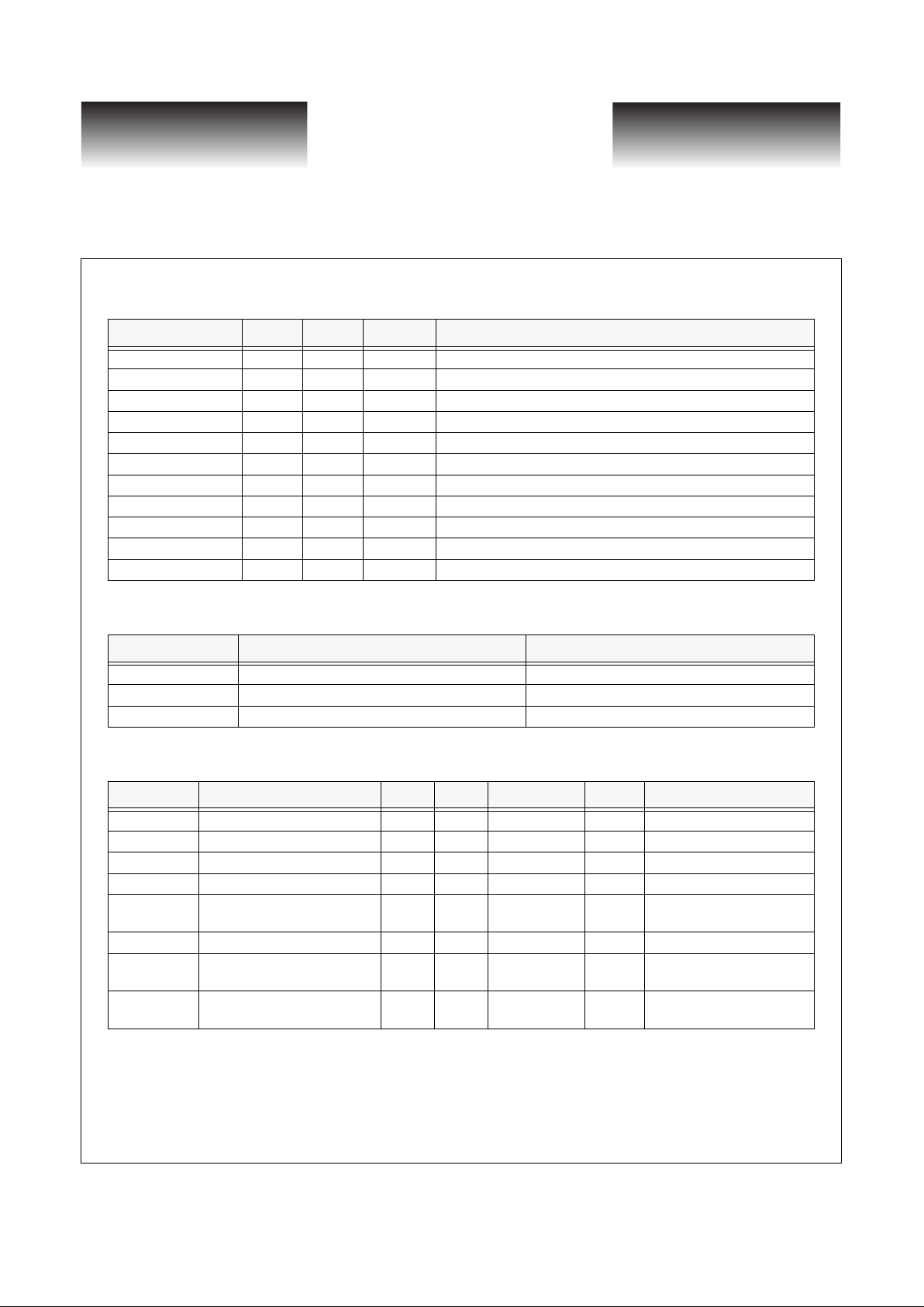
Table 1: Signal Pin Reference
Table 2: Absolute Maximum Ratings
Table 3: Recommended Operating Conditions
Signal
Type Level # Pins Description
DIN In AC 1 Data Input
VREF In DC 1 Data Input Reference
OUT Out AC 1 Laser Modulation Current Output
NOUT Out AC 1 Laser Modulation Current Output (Complementary)
VSS Pwr Pwr 2 Negative Voltage Rail
GND Pwr Pwr 12 Positive Voltage Rail
VIP In DC 1 Modulation Control Node
MIP In DC 1 Modulation Monitor Node
VIB In DC 2 Bias Control Node
MIB In DC 2 Bias Monitor Node
Total Pins 24
Symbol
Rating Limit
V
SS
Negative Power Supply Voltage V
CC
to -6.0V
T
j
Maximum Junction Temperature -55 ° C to + 125 ° C
T
stg
Storage Temperature -65 ° C to +150 ° C
Symbol
Parameter Min Typ Max Units Conditions
GND Positive V oltage Rail 0 V
VSS Negative Voltage Rail -5.5 -5.2 -4.75 V
VIH HIGH Level Input Voltage -1.0 -0.9 — V VREF = -1.3V
VIL LOW Level Input Voltage — -1.7 -1.6 V VREF = -1.3V
VIB1
VIB2
BIAS Control Voltages VSS VSS +1.1 V
VIP Modulation Control Voltage VSS VSS +1.8 V
θ
jc
Thermal Resistance Junction
to Case
25
°
C/W
T
J
Operational Junction
Temperature
120
°
C

VITESSE
SEMICONDUCTOR CORPORATION
Target Specification
VSC7934
Single Supply 2.5 Gb/s
Voltage Driver
G52181-0, Rev 1.1
VITESSE SEMICONDUCTOR CORPORATION
Page 3
10/14/97 741 Calle Plano, Camarillo, CA 93012 • 805/388-3700 • FAX: 805/987-5896
Table 4: Electrical Specifications (Tc = 25 ° C, VSS = -5.2V, RL = 50 Ω , at OUT
Pin)
Input T ermination Schemes
Figure 1: Input Structure
Symbol
Parameter Min Typ Max Units Conditions
I
NOUT
Maximum Peak Current 60 — — mA
VIP = -4.1V
VIB1 = -5.2V
VIB2 = -5.2V
DIN = “Lo”
I
NOUT
Maximum Peak Current — — 4 mA
VIP = -4.1V
VIB1 = -5.2V
VIB2 = -5.2V
DIN = “Hi”
I
BIAS1,
I
BIAS2
Maximum Bias Current 30 — — mA
VIB2 = -3.4V
VIB1 = -5.2V
VIP = -5.2V
Rise Time — 100 — ps 20% to 80%
Fall Time — 100 — ps 20% to 80%
VREF Reference V oltage — -1.3 — V
Output Voltage — — -3.0 V
VIP = -4.1V
VIB1 = -5.2V
VIB2 = -5.2V
DIN = “Lo”
I
VSS
Power Supply Current (V
SS
)90mA
VSS = -5.2V
VIP = -5.2V
VIB1 = -5.2V
VIB2 = -5.2V
X
X
+
-
2600 2600
7800 7800
OV (GND)
-5.2V (VSS)
DIN
VREF
• Nominal VREF = -1.3V
• 2600, 7800 Ohm Resistors
on die, nominal values
 Loading...