

VITESSE VSC7926W, VSC7926KF, VSC7926KFL Datasheet
VITESSE
SEMICONDUCTOR CORPORATION
Preliminary Data Sheet
VSC7926
SDH/SONET 2.5Gb/s Laser Diode Driver
G52188-0, Rev 3.0 Page 1
04/05/01
© VITESSE SEMICONDUCTOR CORPORATION • 741 Calle Plano • Camarillo, CA 93012
Tel: (800) VITESSE • FAX: (805) 987-5896 • Email: prodinfo@vitesse.com
Internet: www.vitesse.com
Features
General Description
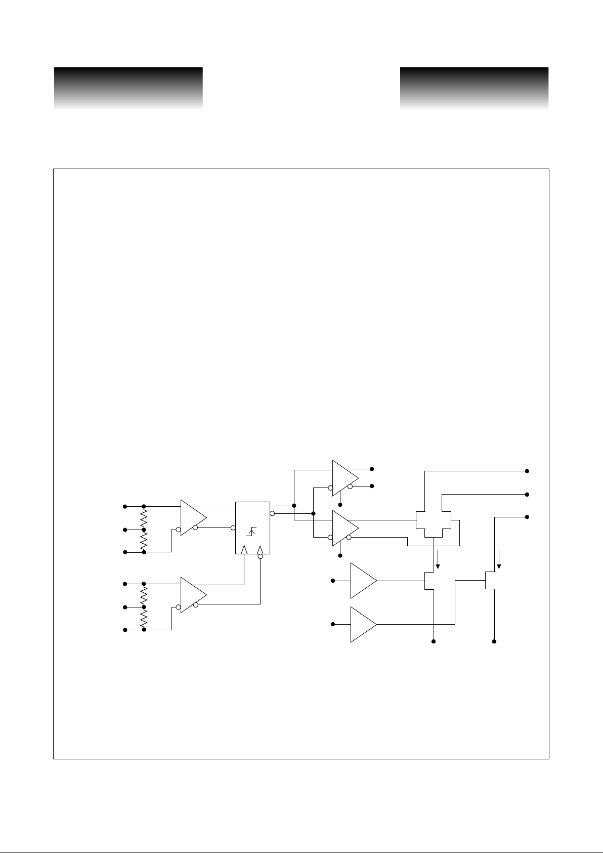
The VSC7926 is a single 5V supply, 2.5Gb/s laser diode driver with direct acce ss to the laser modulation
and bias FETs. Laser bias and modulation currents are set by external components allowing precision monitoring and setting of the current levels. Data density outputs are provided to allow the user to adjust the laser bias
in high unbalanced data applications. Clock and data inputs are differentially terminated to 50
Ω.
Applications
• SDH/SONET @ 622Mb/s, 1.244Gb/s, 2.488Gb/s
• Full Speed Fibre Channel (1.062Gb/s)
VSC7926 Block Diagram
• Rise Times of Less Than 100ps
• High-Speed Operation
(Up to 2.5Gb/s NRZ Data)
• Differential Inputs
• Single Supply
• Direct Access to Modulation and Bias FETs
• Data Density Monitors
• On-Chip Reclocking Register
DIN
DINTERM*
50 Ω
MK
NMK
IBIAS
NIOUT
IOUT
MIP
VIP
VIB
MIB
DQ
DCC
**
**On Die Components
I
MOD
I
BIAS
50 Ω
**
NDIN
CLK
50 Ω
**
50 Ω
**
NCLK
CLKTERM*
*Terminated to Off-chip Capacitor
DCC
VITESSE
SEMICONDUCTOR CORPORATION
Preliminary Data Sheet
VSC7926
SDH/SONET 2.5Gbits /sec
Laser Diode Driver
Page 2 G52188-0, Rev 3.0
04/05/01
© VITESSE SEMICONDUCTOR CORPORATION • 741 Ca ll e Pl an o • Camarillo, CA 93012
Tel: (800) VITESSE • FAX: (805) 987-5896 • Email: prodinfo@vitesse.com
Internet: www.vitesse.com
Table 1: Signal Pin Reference
Table 2: Absolute Maximum Ratings
Table 3: High Speed Inputs and ECL Outputs
Signal Type Level # Pins Description
DIN, NDIN In 2 Data Input and Data Reference
DINTERM Ref DC 1 Data Termination
CLKTERM Ref DC 1 Clock Termination
MK, NMK Out ECL 2 Data Density Differential Outputs
NIOUT Out 1 Laser Modulation Current Output (Complementary)
IOUT Out 1 Laser Modulation Current Output (To Laser Cathode)
VSS Pwr Pwr 3 Negative Voltage Rail
GND Pwr Pwr 5 Positive Voltage Rail
VIP In DC 1 Modulation Gate Node
MIP In DC 1 Modulation Source Node
VIB In DC 1 Bias Gate Node
MIB In DC 1 Bias Sour ce Node
IBIAS Out DC 1 Laser Bias Output (To Laser Cathode)
CLK, NCLK In 2 Clock Input and Clock Reference
DCC In DC 1 Duty Cycle Control, Leave Floating
T otal Pin s 24
Symbol Rating Limit
V
SS
Negative Power Supply Voltage VCC to -6.0V
T
j
Maximum Junction Temperature -55°C to + 125°C
T
stg
Storage Temperature -65°C to +150°C
Symbol Parameter Min Max Units Conditions
V
IN
Differential Input Voltage Swing 500 1000 mV
V
CM
Differential Input Common Mode Range -2.3 -1.3 V VSS = -5.2V
V
OH
ECL Output High Voltage -1200 mV 50Ω to -2.0V
V
OL
ECL Output Low Voltage -1600 mV 50Ω to -2.0V
VITESSE
SEMICONDUCTOR CORPORATION
Preliminary Data Sheet
VSC7926
SDH/SONET 2.5Gb/s Laser Diode Driver
G52188-0, Rev 3.0 Page 3
04/05/01
© VITESSE SEMICONDUCTOR CORPORATION • 741 Calle Plano • Camarillo, CA 93012
Tel: (800) VITESSE • FAX: (805) 987-5896 • Email: prodinfo@vitesse.com
Internet: www.vitesse.com
Table 4: Recommended Operating Conditions
NOTES: (1) Lower limit of specification is ambient temperature and upper limit is case temperature. (2) See “Calculation of the
Maximum Case Temperature” section in this data sheet for detailed maximum temperature calculations.
Table 5: Power Dissip atio n
Table 6: Laser Driver DC Electrical Specifications
Table 7: Laser Driver AC Electrical Specifications
Table 8: Package Thermal Specifications
Symbol Parameter Min Typ Max Units Conditions
GND Positive Voltage Rail - 0 - V
VSS Negative Voltage Rail -5.5 -5.2 -4.9 V
Tc
l
Operational Temperature
(1)
-40 - 85
(2)
°C Power dissipation = 1.25W
T
J
Junction Temperature - - 125 °C
Symbol Parameter Min Typ Max Units Conditions
I
VSS
Power Supply Current (VSS) - - 220 mA VSS = -5.5, I
MOD
= I
BIAS
= 0mA
P
D
T otal Po wer Dissipatio n - - 1210 mW
V
SS
= -5.5, I
MOD
= I
BIAS
= 0mA,
R
LOAD
= 25Ω to GND
P
DMAX
Maximum Power Dissipation - - 1815 mW
V
SS
= -5.5, I
MOD
= 60mA,
I
BIAS
= 50mA, I
OUT
= 0V
Symbol Parameter Min Typ Max Units Conditions
I
BIAS
Programmable Laser Bias Current 2 - 50 mA
I
MOD
Programmable Modulation Current 2 - 60 mA
V
IB
Laser Bias Control Voltage - -
V
SS
+
2.1
VI
BIAS
= 50mA
V
IP
Laser Modulation Control Voltage - -
V
SS
+
2.1
VI
MOD
= 60mA
V
OCM
Output Voltage Compliance
GND
-2.5V
--VV
SS
= -5.2V
Symbol Parameter Min Typ Max Units Conditions
tR t
F
Output Rise and Fall Times - - 100 ps
25Ω load, 20%-80%,
15mA < I
MOD
< 60 mA,
I
BIAS
= 40mA
t
SU
Setup Data to Clock Setup Time - 50 - ps
t
H
Hold Time - 50 - ps
Symbol Parameter Min Typ Max Units Conditions
θ
JCC
Thermal Resistance from Junction-to-Case - 25 - °C/W Ceramic Package
 Loading...