

VITESSE VSC7809X, VSC7809WC, VSC7809WD, VSC7809WB, VSC7809WA Datasheet
VITESSE
SEMICONDUCTOR CORPORATION
Advance Product Information
VSC7809
Photodetector/Transimpedance Amplifier
Family for Optical Communication
Features
• Integrated Photodetector/Transimpedance
Amplifier Optimized for High-Speed Optical
Communications Applications
• Fibre Channel/Gigabit Ethernet Compatible
• High Bandwidth
Part Number Data Rate
VSC7809 1.25Gb/s 800 1.4 100
Bandwidth
(MHz)
• Low Input Noise Equivalent Power
• Large Optically Active Area
• Single 3.3V Power Supply
Input Noise
µW rms)
(
Optically Active Area
µm diameter)
(
General Description
The VSC7809 integrated Photodetector/Transimpedance Amplifier provides a highly integrated solution
for converting light from a fiber optic communications channel into a differential output voltage. The benefits
of V itesse S emiconduct or’ s Galliu m Arsenide H- GaAs process ar e fully ut ilized to prov ide very high b andwidth
and low noise in a product with a large optically active area for easy alignment. The sensitivity, duty cycle distortion and jitter meet or exceed all Fibre Channel and Gigabit Ethernet application requirements. Par ts are
available in either die form, flat-windowed packages or in ball-lens packag es.
By using a metal-semiconductor-metal (MSM) photodetector with a monolithic integrated transimpedance
amplifier , t he in put capac it ance is lowered which allows for a larger optica ll y act i ve ar ea t han in di scr et e phot odetectors. Integration also allows superior tracking over process, temperature and voltage between the photodetector and the amplifier, resulting in higher performance. This part can easily be used in developing Fibre
Channel Electro-Optic Receivers which exhibit very high performance and ease of use.
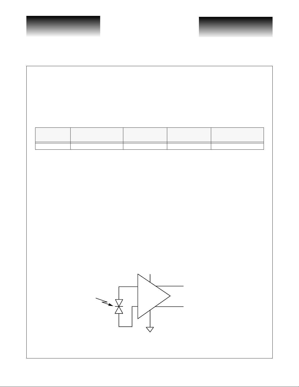
VSC7809 Block Diagram
Photodetector/Transimpedance Amplifier
+3.3V
DOUTP
DOUTN
GND
Both DOUTP and DOUTN are back-terminated to 25Ω.
G52195-0, Rev 2.4 Page 1
04/05/01
© VITESSE SEMICONDUCTOR CORPORATION • 741 Calle Plano • Camarillo, CA 93012
Tel: (800) VITESSE • FAX: (805) 987-5896 • Email: prodinfo@vitesse.com
Internet: www.vitesse.com
VITESSE
SEMICONDUCTOR CORPORATION
Photodetector/Transimpedance Amplifier
Advance Product Information
Family for Optical Communication
Table 1: Electro-Optical Specifications
Symbol Parameter Min Typ
V
SS
I
DD
PSRR Power Supply Rejection Ratio - -10 - dB
λ Wavelength 700 840 850 nm
f
C
BW Optical Modulation Bandwidth 800 1100 - MHz
S Sensitivity -20 -21 dBm 1.25Gb/s, BER10
R
O
V
O
R
D
V
DC
∆V
DC
NEP
V
NO
DCD Duty Cycle Distortion - - 4.5 % P = -5dBm
I
OUT
PDJ Pattern Dependent Jitter - 35 60 ps
---- Optically Active Area - 100 - µm Diameter
PPJ PP Jitter - 190 250 ps P = -5 dBm
t
R
t
F
Supply Voltag e 3.0 3.3 3.6 V
Supply Current 14 23 40 mA
Low Frequency Cut off - 1.8 2.5 MHz
Single Ended Output Impedance 20 25 30 Ω
Differential Output Voltage 0.2 0.26 0.4 V
Differential Responsivity 0.8 1.2 - mV/µW
Output Bias Voltage 1.0 - - V
Bias Offset Voltage - - 200 mV
Input Noise Equivalent Power - 1 1.4 µW rms P = 0mW
O
Output Noise Voltage - 1.0 1.25 mV rms P = 0mW
Output Drive Current 2.0 2.6 - mA P = -5dBm
Rise Time - - 400 ps 20%-80% P = -5dBm
Fall Time - - 400 ps 20%-80% P = -5dBm
(1)
(2)
Max Units Conditions
Frequencies up to 40MHz
Use external filter to get
PSRR of -35dB
-3db, P
50MHz
-3db,
P = -15dBm @ 50MHz
P = -5dBm,
R
LOAD
R
LOAD
P = -15dBm @ 50MHz
P = -5dBm
+/-10% Voltage Window
VSC7809
(3)
.
(4)
= -15dBm @
-12(5)
= 100Ω differential
= 100Ω
Notes: (1) Specified over 0°C (ambient) to 70°C (case).
(2) Typical conditions 25°C and 3.3V power supply.
(3) See Note 1 in Application Note 48.
(4) P = Incident Optical Power
(5) See Note 2 In Application Note 48.
Page 2 G52195-0, Rev 2.4
© VITESSE SEMICONDUCTOR CORPORATION • 741 Ca l le Pl an o • Camarillo, CA 93012
Tel: (800) VITESSE • FAX: (805) 987-5896 • Email: prodinfo@vitesse.com
Internet: www.vitesse.com
04/05/01
VITESSE
SEMICONDUCTOR CORPORATION
Advance Product Information
VSC7809
Photodetector/Transimpedance Amplifier
Family for Optical Communication
Table 2: Absolute Maximum Ratings
Symbol Parameter Limits
V
SS
T
STG
H
STG
H
OP
P
INC
IS Impact Shock
V
IB
Power Supply 6V Required
Storage Temperature -55°C to 125°C (case temperature under bias)
Storage Humidity 5 to 95% R.H. (including condensation )
Operating Humidity 8 to 80% R.H. (excluding condensation)
Incident Optical P ower +3dBm
500 G. Half Sine Wave
Pulse Duration 1 +/-0.5 ms
3 blows in each direction
20 > 2000 > 20Hz, 10 Minutes
Vibration
10 G. Peak Acceleration
4 Complete Cycles, 3 Perpendicular Axes
Table 3: Recommended Operating Conditions
Symbol Parameter Limits
V
T
P
SS
OP
MAX
Power Supply 3.0VP-3.6V (3.3V nominal)
Operating Temperature 0°C (ambient) to 70°C (case)
Maximum Optical Power 0dBm
G52195-0, Rev 2.4 Page 3
04/05/01
© VITESSE SEMICONDUCTOR CORPORATION • 741 Calle Plano • Camarillo, CA 93012
Tel: (800) VITESSE • FAX: (805) 987-5896 • Email: prodinfo@vitesse.com
Internet: www.vitesse.com
 Loading...