

VITESSE VSC7711X Datasheet

VITESSE SEMICONDUCTOR CORPORATION
Page 1
10/6/99 741 Calle Plano, Camarillo, CA 93012 • 805/388-3700 • FAX: 805/987-5896
VITESSE
SEMICONDUCTOR CORPORATION
dvance Product Information
SC7711
Transimpedance Amplifier
Family for Optical Communication
G52178-0, Rev. 2.1
Features
• Transimpedance Amplifier optimized for
high speed optical communications applications
• Integrated AGC
• Fibre Channel and Gigabit Ethernet
• Low Input Noise Current
• Differential Output
• Single 5V Supply with On-chip biasing
for photodetectors
General Description
The VSC7711 Transimpedance Amplifiers provide a high performance solution for amplifying high speed
photodetector output signals from a fiber optic communications channel into a differential output voltage. The
benefits of Vitesse Semiconductor’s Gallium Arsenide H-GaAs III process are fully utilized to provide a very
high bandwidth and low noise amplifier. The detector bias is supplied on-chip eliminating the need for a separate bias connection. The sensitivity, duty cycle distortion and jitter meet or exceed all Fibre Channel and Gigabit Ethernet requirements.
In conjunction with suitable photodetectors, these parts can be easily used in developing a wide range of
Fibre Channel and Gigabit Ethernet optoelectronic receivers for both short wavelength (850nm) as well as long
wavelength (1300nm) applications.
Part Number
Data Rate
(Gb/s)
Bandwidth
(MHz)
Transimpedance
(k
Ω)
Input Noise
(nA RMS)
VSC7711 1.25 800 3.5 180
D0
D1
+5V
Block Diagram:
Photodetector/Transimpedance Amplifier
+
_
VITESSE
SEMICONDUCTOR CORPORATION
Advance Product Information
VSC7711
Transimpedance Amplifier
Family for Optical Communication
Page 2
VITESSE SEMICONDUCTOR CORPORATION
G52178-0, Rev 2.1
741 Calle Plano, Camarillo, CA 93012 • 805/388-3700 • FAX: 805/987-5896 10/6/99
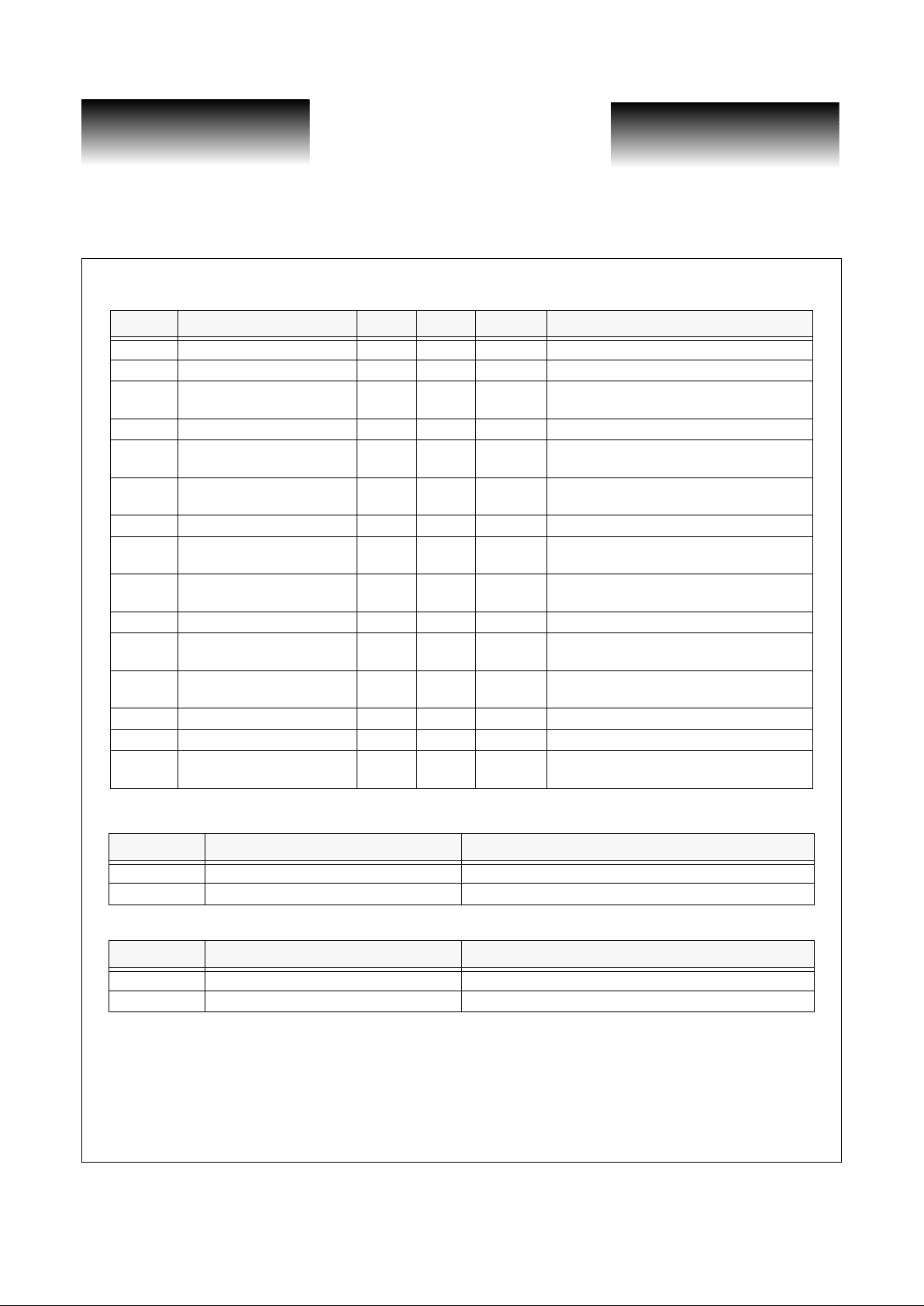
Table 1: Electrical Characteristics of Transimpedance Amplifiers
(VS = 5V & T = 25°C unless otherwise noted)
Table 2: Absolute Maximum Ratings
Table 3: Recommended Operating Conditions
Symbol Parameter Min. Max. Units Conditions
V
DD
Supply Voltage 4.5 5.5 V —
I
s
Supply Current — 62 mA I
in
4µApp to 1.5mA
pp
BW
Optical Modulation
Bandwidth
800 MHz I
in
= 20µA
pp,
detector capacitance = 0.6pf
F
c
Low Frequency Cutoff 1.5 MHz I
in
= 20µA
pp
Tr, T
f
Output Rise & Fall Time — 250 ps
20% to 80%
I
in
-1.0mA
pp
R
d
Differential Transresistance 3.5 — kΩ
R
L
= 100Ω, differential
I
in
= 20µA
I
max
Output Drive Current 1.5 — mA
pp
10% Duty Cycle Distortion
I
n
Input Noise Equivalent
Current
— 180 nA RMS BW = 800 MHz
I
n
Input Noise Equivalent
Current Spectral Density
—6.4pA/ √Hz BW = 800 MHz
PDJ Pattern Dependent Jitter — 60 ps
R
o
Single Ended Output
Impedance
25 75 Ω —
V
max
Maximum Differential
Output Voltage
—700MV
pp
I
in
= 1.0mA
pp
RL = 100Ω, differential
V
B
Output Bias Voltage 0.5 1.7 V —
V
off
Output Offset Voltage 0.15 V —
PSRR
Power Supply Rejection
Ratio
35 — dB f = 0.3MHz - 40MHz, with external filter
Symbol Parameter Limits
V
DD
Power Supply 6V
T
stg
Storage Temperature -55°C to 125°C (die temperature under bias)
Symbol Parameter Limits
V
DD
Power Supply 4.5-5.5V (5.0V nominal)
T
op
Operating Temperature 0°C (ambient) to 80°C (die)
VITESSE SEMICONDUCTOR CORPORATION
Page 3
10/6/99 741 Calle Plano, Camarillo, CA 93012 • 805/388-3700 • FAX: 805/987-5896
VITESSE
SEMICONDUCTOR CORPORATION
dvance Product Information
SC7711
Transimpedance Amplifier
Family for Optical Communication
G52178-0, Rev. 2.1
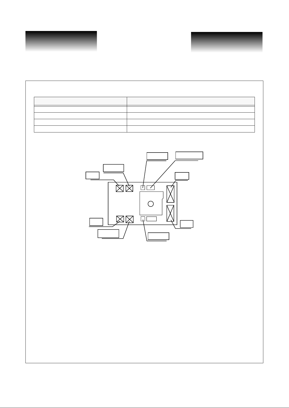
Table 4: Pin Table Specifications for Bare Die
Figure 1: Schematic View of Bare Die Pad Assignments
Note: Refer to Figure 4 for die layout detail.
Symbol Description
D
+
OUT
Data output normal (with reference to incident light)
D
–
OUT
Data output complement (inverting) (with referenc e to incid ent lig ht)
VDD Power supply
GND Ground (package case)
GND
GND
ANODE
ANODE
CATHODE
D
+
OUT
D
–
OUT
VDD
VDD
 Loading...